EP0551737A1 - Vapor deposition process for coating articles of manufacture - Google Patents
Vapor deposition process for coating articles of manufacture Download PDFInfo
- Publication number
- EP0551737A1 EP0551737A1 EP92311256A EP92311256A EP0551737A1 EP 0551737 A1 EP0551737 A1 EP 0551737A1 EP 92311256 A EP92311256 A EP 92311256A EP 92311256 A EP92311256 A EP 92311256A EP 0551737 A1 EP0551737 A1 EP 0551737A1
- Authority
- EP
- European Patent Office
- Prior art keywords
- coating
- performing step
- coating method
- manufacture
- depositing
- Prior art date
- Legal status (The legal status is an assumption and is not a legal conclusion. Google has not performed a legal analysis and makes no representation as to the accuracy of the status listed.)
- Granted
Links
Images
Classifications
-
- C—CHEMISTRY; METALLURGY
- C23—COATING METALLIC MATERIAL; COATING MATERIAL WITH METALLIC MATERIAL; CHEMICAL SURFACE TREATMENT; DIFFUSION TREATMENT OF METALLIC MATERIAL; COATING BY VACUUM EVAPORATION, BY SPUTTERING, BY ION IMPLANTATION OR BY CHEMICAL VAPOUR DEPOSITION, IN GENERAL; INHIBITING CORROSION OF METALLIC MATERIAL OR INCRUSTATION IN GENERAL
- C23C—COATING METALLIC MATERIAL; COATING MATERIAL WITH METALLIC MATERIAL; SURFACE TREATMENT OF METALLIC MATERIAL BY DIFFUSION INTO THE SURFACE, BY CHEMICAL CONVERSION OR SUBSTITUTION; COATING BY VACUUM EVAPORATION, BY SPUTTERING, BY ION IMPLANTATION OR BY CHEMICAL VAPOUR DEPOSITION, IN GENERAL
- C23C16/00—Chemical coating by decomposition of gaseous compounds, without leaving reaction products of surface material in the coating, i.e. chemical vapour deposition [CVD] processes
- C23C16/22—Chemical coating by decomposition of gaseous compounds, without leaving reaction products of surface material in the coating, i.e. chemical vapour deposition [CVD] processes characterised by the deposition of inorganic material, other than metallic material
- C23C16/30—Deposition of compounds, mixtures or solid solutions, e.g. borides, carbides, nitrides
-
- G—PHYSICS
- G02—OPTICS
- G02B—OPTICAL ELEMENTS, SYSTEMS OR APPARATUS
- G02B1/00—Optical elements characterised by the material of which they are made; Optical coatings for optical elements
- G02B1/10—Optical coatings produced by application to, or surface treatment of, optical elements
- G02B1/11—Anti-reflection coatings
-
- C—CHEMISTRY; METALLURGY
- C23—COATING METALLIC MATERIAL; COATING MATERIAL WITH METALLIC MATERIAL; CHEMICAL SURFACE TREATMENT; DIFFUSION TREATMENT OF METALLIC MATERIAL; COATING BY VACUUM EVAPORATION, BY SPUTTERING, BY ION IMPLANTATION OR BY CHEMICAL VAPOUR DEPOSITION, IN GENERAL; INHIBITING CORROSION OF METALLIC MATERIAL OR INCRUSTATION IN GENERAL
- C23C—COATING METALLIC MATERIAL; COATING MATERIAL WITH METALLIC MATERIAL; SURFACE TREATMENT OF METALLIC MATERIAL BY DIFFUSION INTO THE SURFACE, BY CHEMICAL CONVERSION OR SUBSTITUTION; COATING BY VACUUM EVAPORATION, BY SPUTTERING, BY ION IMPLANTATION OR BY CHEMICAL VAPOUR DEPOSITION, IN GENERAL
- C23C16/00—Chemical coating by decomposition of gaseous compounds, without leaving reaction products of surface material in the coating, i.e. chemical vapour deposition [CVD] processes
- C23C16/44—Chemical coating by decomposition of gaseous compounds, without leaving reaction products of surface material in the coating, i.e. chemical vapour deposition [CVD] processes characterised by the method of coating
- C23C16/458—Chemical coating by decomposition of gaseous compounds, without leaving reaction products of surface material in the coating, i.e. chemical vapour deposition [CVD] processes characterised by the method of coating characterised by the method used for supporting substrates in the reaction chamber
-
- G—PHYSICS
- G02—OPTICS
- G02B—OPTICAL ELEMENTS, SYSTEMS OR APPARATUS
- G02B5/00—Optical elements other than lenses
- G02B5/08—Mirrors
- G02B5/0808—Mirrors having a single reflecting layer
Definitions
- any suitable coating material for example a metal such as aluminum or tungsten deposited from an organo-metallic precursor, may be used to form a reflective coating utilizing the vapor deposition method of the present invention.
Landscapes
- Chemical & Material Sciences (AREA)
- Physics & Mathematics (AREA)
- Mechanical Engineering (AREA)
- Metallurgy (AREA)
- General Chemical & Material Sciences (AREA)
- Chemical Kinetics & Catalysis (AREA)
- Engineering & Computer Science (AREA)
- Materials Engineering (AREA)
- Organic Chemistry (AREA)
- Optics & Photonics (AREA)
- General Physics & Mathematics (AREA)
- Inorganic Chemistry (AREA)
- Chemical Vapour Deposition (AREA)
- Surface Treatment Of Glass (AREA)
- Glass Compositions (AREA)
- Surface Treatment Of Optical Elements (AREA)
- Physical Vapour Deposition (AREA)
- Optical Elements Other Than Lenses (AREA)
Abstract
Description
- The present invention relates to a method of applying a coating to articles of manufacture and, more particularly, to a vapor deposition process for the application of such a coating.
- In the past, spherical lenses have been coated with an anti-reflective (AR) material such as MgF₂, SiO₂, or other physical vapor deposited films. In particular, the spherical lenses would be loaded into a fixture and inserted in a barrel coating machine. The fixture would then be physically rotated to coat the spheres with the AR material. In order to coat both sides of the spheres, the process must be shut down and the fixture turned over. As a result, this coating process leaves a ring of uncoated surface around the middle of the device. Thus, when later utilizing the lens, orientation must be carefully controlled such that the uncoated ring portion is displaced out of the optical signal path. Another problem with the physical vapor deposition approach is the lack of uniformity of the AR coating, where this lack of uniformity affects the coupling efficiency of the lens. Further, the relatively small diameter of an individual sphere (for example, ≦300µm) and the fragility of such a lens when fabricated out of certain materials (such as glass), results in a significant number of lenses being irreparably damaged during the coating process.
- Therefore, a need remains in the art for a method of applying a uniform coating, such as an AR coating, to an article of manufacture, such as a spherical lens member.
- The need remaining in the prior art is addressed by the present invention which relates to a method of applying a coating to an article of manufacture and, more particularly, to a vapor deposition process for the application of such a coating as defined by the appended claims.
- In one exemplary embodiment of the present invention, a plurality of articles are loaded onto a carrier and subjected to chemical vapor deposition (CVD) of a suitable material for a time and temperature sufficient to provide a substantially uniform coating of the desired thickness. The uniformity is achieved by utilizing CVD processes that favor heterogeneous film growth (which are minimally affected by gas flow dynamics) as compared to gas phase reactions and processes.
- For a specific embodiment, the articles may comprise spherical members. When utilized with spheres, a carrier may be formed to include a grid of trenches in the top surface thereof such that the lenses may be placed upon the top surface and rest upon only four individual points of contact (the contacts being << 1 µm and formed by the intersection of the trenches). The utilization of such a carrier results in coating essentially the entire outer surface of each spherical member. Spheres of various sizes may be simultaneously coated. In fact, a number of separate carriers, each including grids for supporting lenses of different sizes, may be processed simultaneously.
- When utilized to apply an AR coating to a plurality of spherical lenses, the method may employ the chemical vapor deposition of an SiO₂ material such as DADBS (diacetoxyditertiarybutoxysilane). Advantageously, the method of the present invention may also be utilized to apply a reflective coating to a spherical member. In this case, the thickness of the deposited material is chosen to provide the desired degree of reflectivity. Alternatively, metals may be deposited from organometallic precursors to yield reflective metallic films.
- An advantage of the technique of the present invention is that a large number of articles of manufacture may be simultaneously processed to form a coating layer with a predetermined uniformity, the CVD process resulting in an extremely high yield for the coated articles.
- Other and further advantages of the present invention will become apparent during the course of the following discussion and by reference to the accompanying drawings.
-
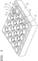
- FIG. 1 illustrates a plurality of exemplary articles of manufacture, in the form of lenses, disposed on a carrier suitable for use in the method of the present invention;
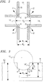
- FIG. 2 is a top view of a portion of the arrangement of FIG. 1; and
- FIG. 3 is a cut-away side of the arrangement of FIG. 1.
- FIG. 1 illustrates a plurality of
spherical lenses 10 as positioned upon acarrier member 12 suitably formed to be used in association with the inventive method. It is to be understood that the coating process to be described hereinbelow is suitable for use with any desired article of manufacture and the following discussion directed to spherical members is for exemplary purposes only. Referring back to FIG. 1,member 12 contains a plurality of "horizontal"trenches 14 and a plurality of "vertical"trenches 16 formed intop surface 18 ofmember 12. The pluralities of trenches intersect to form the grid-like structure as shown in FIG. 1. The dimensions and spacing oftrenches lenses 10 will rest therebetween with only four points of contact, denoted A, B, C and D in FIG. 1. As will be discussed hereinafter in association with FIGs. 2 and 3,trenches spheres 10 incarrier 12. - After
spherical lenses 10 are loaded oncarrier 12,carrier 12 is inserted in a reactor chamber (not shown) to begin the chemical vapor deposition of the coating material. Once the coating has been deposited to the desired thickness (as determined by processing parameters such as time and ambient temperature), the carrier is removed from the chamber. Coatedlenses 10 may then be removed fromcarrier 12, using a "pick and place" tool, for example. Although points of contact A, B, C and D will not be coated, such has not been found to affect the optical properties of the coated lens, perhaps due to the relatively small contact point size (e.g., << 1 µm for a 300 µm sphere). It is to be noted that spheres of various dimensions may be simultaneously contacted and, further, several carriers may be processed simultaneously to further increase throughput. - Approximately 1000 sapphire spheres, each approximately 300µm in diameter, were loaded onto a carrier (approximately one inch square) as depicted in FIG. 1. The loaded carrier was transferred into a reactor chamber and a DADBS SiO₂ layer was deposited. In practice, one reactor chamber may easily handle 10 to 50 carriers during each run. The chamber was maintained at a temperature of approximately 500°C and the deposition was performed for approximately 26.5 minutes. The time and temperature parameters were calculated to yield an AR coating layer (for λ = 1.3 µm) approximately 225 nm thick.
- Ellipsometry measurements on coated witness slides yielded an actual thickness of approximately 222 nm. Optical transmission and reflection measurements on the spheres gave results consistent with theory (i.e., transmissivity > 98% and reflectivity < 1%). Under optical microscope examination, no contact points were visible (with magnification greater than 400x). Measurements of several thousand spheres yielded spheres with transmissivity greater than 98%, regardless of orientation.
- It has been found, through experimentation, that improved stability of spheres on the trench structure of
carrier 12 may result from the utilization of sets of bi-level trenches, as illustrated in particular in FIGs. 2 and 3. In the top view of FIG. 2, anexemplary sphere 10i,j is illustrated as resting in the intersection ofhorizontal trench 14i andvertical trench 16j. Each trench, in actuality, comprises a lower trench of width w₁ and an upper trench of width w₂, where w₁ is less than w₂. The widths are chosen such that a sphere of diameter D rest upon four points of contact A, B, C and D (A and B being the only visible points of contact in FIG. 3). The difference in width being chosen such that only slight motion of the spheres (indicated by the arrows in FIG. 2) will be tolerated before the spheres contact points A', B', C'or D' associated with the upper trenches. - As seen by the view in FIG. 3, lower horizontal trench 14'i is formed to comprise a depth d₁ below
top surface 18 ofcarrier 12. This depth is chosen such that sufficient flow of material through the trench during the CVD coating process is maintained. Depth d₂ for upper trench 14''i may be chosen such that approximately half ofsphere 10i,j remains abovesurface 18 ofcarrier 12. - It is to be noted that the above-described technique is equally applicable to forming a reflective coating on an article of manufacture, where such a reflective coating may be useful for some applications. Any suitable coating material, for example a metal such as aluminum or tungsten deposited from an organo-metallic precursor, may be used to form a reflective coating utilizing the vapor deposition method of the present invention.
Claims (16)
- A method of coating a plurality of articles of manufacture comprising the steps of:a) providing a plurality of articles of manufacture (10);b) loading said plurality of articles of manufacture onto a carrier support member (12);c) inserting the loaded carrier support member into a reactor chamber; andd) depositing, using a chemical vapor deposition process, a suitable coating material onto the exposed surface of each article of manufacture, the deposition performed at a predetermined temperature and for a predetermined time sufficient to form an essentially uniform coating of the desired thickness.
- A coating method as defined in claim 1 wherein in performing step d), depositing an anti-reflective coating material as the suitable coating material.
- A coating method as defined in claim 2 wherein in performing step d), depositing a coating of silicon dioxide.
- A coating method as defined in claim 3 wherein in performing step d), DADBS is utilized to form the silicon dioxide.
- A coating method as defined in claim 3 wherein in performing step d), the predetermined deposition temperature is approximately 500 °C.
- A coating method as defined in claim 5 wherein in performing step d), the deposition is performed for a predetermined time sufficient to form a coating in the range of 200-300 nm.
- A coating method as defined in claim 6 wherein the predetermined time is in the range of 20-30 minutes.
- A coating method as defined in claim 1, wherein in performing step d), depositing a reflective coating.
- A coating method as defined in claim 8 wherein in performing step d), depositing a metallic coating from an organo-metallic precursor.
- A coating method as defined in claim 9 wherein in performing step d), aluminum is deposited.
- A coating method as defined in claim 1 wherein in performing step a), a plurality of spherical members is provided.
- A coating method as defined in claim 11 wherein in performing step b), loading the spherical members onto a carrier comprising a grid of intersecting trenches formed in the top surface thereof such that each spherical member is disposed at an intersection of a pair of trenches and is supported by four points of contact with said carrier.
- A coating method as defined in claim 12 wherein in performing step b), the intersecting trenches are bi-level in form, comprising a lower trench of width w₁ and an upper trench of width w₂, where w₁ < w₂.
- A coating method as defined in claim 11 wherein in performing step a), a plurality of spherical lenses is provided.
- A coating method as defined in claim 11 wherein in performing step a), a plurality of sapphire lenses is provided.
- A coating method as defined in claim 11 wherein in performing step d), depositing an anti-reflective coating material.
Applications Claiming Priority (2)
| Application Number | Priority Date | Filing Date | Title |
|---|---|---|---|
| US80870491A | 1991-12-13 | 1991-12-13 | |
| US808704 | 1991-12-13 |
Publications (2)
| Publication Number | Publication Date |
|---|---|
| EP0551737A1 true EP0551737A1 (en) | 1993-07-21 |
| EP0551737B1 EP0551737B1 (en) | 1996-05-15 |
Family
ID=25199476
Family Applications (1)
| Application Number | Title | Priority Date | Filing Date |
|---|---|---|---|
| EP92311256A Expired - Lifetime EP0551737B1 (en) | 1991-12-13 | 1992-12-10 | Vapor deposition process for coating articles of manufacture |
Country Status (5)
| Country | Link |
|---|---|
| US (1) | US5380551A (en) |
| EP (1) | EP0551737B1 (en) |
| JP (1) | JP2513976B2 (en) |
| KR (1) | KR950012813B1 (en) |
| DE (1) | DE69210792T2 (en) |
Cited By (2)
| Publication number | Priority date | Publication date | Assignee | Title |
|---|---|---|---|---|
| WO1995025829A1 (en) * | 1994-03-18 | 1995-09-28 | Sandvik Ab | Batch loading system for cvd |
| WO2013158067A1 (en) * | 2012-04-16 | 2013-10-24 | The Timken Company | Method and table assembly for applying coatings to spherical components |
Families Citing this family (11)
| Publication number | Priority date | Publication date | Assignee | Title |
|---|---|---|---|---|
| US5792423A (en) * | 1993-06-07 | 1998-08-11 | Markelov; Michael | Headspace autosampler apparatus and method |
| US5874127A (en) * | 1995-08-16 | 1999-02-23 | Ciba Vision Corporation | Method and apparatus for gaseous treatment |
| US6017581A (en) * | 1997-04-18 | 2000-01-25 | Semi-Alloys Company | Method for coating lenticular articles |
| US6210546B1 (en) * | 1998-10-29 | 2001-04-03 | Lucent Technologies Inc. | Fixture with at least one trough and method of using the fixture in a plasma or ion beam |
| JP4836102B2 (en) * | 2000-06-30 | 2011-12-14 | Hoya株式会社 | Optical element positioning member, optical element positioning member manufacturing method, optical unit, optical unit manufacturing method, lens chip, and floating head for optical memory medium |
| US20030021572A1 (en) * | 2001-02-07 | 2003-01-30 | Steinberg Dan A. | V-groove with tapered depth and method for making |
| US7036944B2 (en) | 2002-04-11 | 2006-05-02 | 3M Innovative Properties Company | Retrochromic articles |
| US6978896B2 (en) * | 2002-04-11 | 2005-12-27 | 3M Innovative Properties Company | Method of making retrochromic beads and kit thereof |
| US7294360B2 (en) * | 2003-03-31 | 2007-11-13 | Planar Systems, Inc. | Conformal coatings for micro-optical elements, and method for making the same |
| JP5622219B2 (en) * | 2008-11-06 | 2014-11-12 | Ntn株式会社 | Spherical surface treatment jig, spherical surface treatment method, and spherical part manufacturing method |
| JP2017503924A (en) | 2013-12-27 | 2017-02-02 | スリーエム イノベイティブ プロパティズ カンパニー | Uniform chemical vapor deposition coating on a 3D array of uniformly shaped articles |
Citations (7)
| Publication number | Priority date | Publication date | Assignee | Title |
|---|---|---|---|---|
| JPS5972127A (en) * | 1982-10-18 | 1984-04-24 | Toshiba Corp | Grooved hot plate for vapor growth |
| JPS6025281A (en) * | 1983-07-22 | 1985-02-08 | Nec Corp | Light emitting light receiving element |
| US4521088A (en) * | 1982-06-17 | 1985-06-04 | Smiths Industries Public Limited Company | Optical element having a catalytic coating to promote oxidation of optically-opaque substances |
| JPS61138201A (en) * | 1984-12-11 | 1986-06-25 | Matsushita Electric Ind Co Ltd | Manufacturing method of spherical lens with anti-reflection coating film |
| JPS6333571A (en) * | 1986-07-25 | 1988-02-13 | Nippon Telegr & Teleph Corp <Ntt> | Film formation method for spherical objects |
| JPH01300528A (en) * | 1988-05-30 | 1989-12-05 | Fujitsu Ltd | Thin-film forming method |
| US5098483A (en) * | 1989-09-05 | 1992-03-24 | Spire Corporation | Methods of treating spherical surfaces |
Family Cites Families (11)
| Publication number | Priority date | Publication date | Assignee | Title |
|---|---|---|---|---|
| US2026203A (en) * | 1934-07-05 | 1935-12-31 | Ackles Hornkohl Company | Icing mechanism |
| US4415512A (en) * | 1979-07-20 | 1983-11-15 | Torobin Leonard B | Method and apparatus for producing hollow metal microspheres and microspheroids |
| USRE30626E (en) * | 1979-09-14 | 1981-05-26 | Ultramet of Pacoima | Spheres obtained by vapor deposition for use in ball point pens |
| US4361111A (en) * | 1981-12-23 | 1982-11-30 | Groen Henry J | Golf ball dry rack |
| JPH0635657B2 (en) * | 1985-05-03 | 1994-05-11 | アメリカン テレフオン アンド テレグラフ カムパニ− | Method for manufacturing device having patterned aluminum layer |
| US4725890A (en) * | 1986-07-15 | 1988-02-16 | Ovonic Imaging Systems, Inc. | Flexible array of photosensitive elements |
| US4704298A (en) * | 1986-07-31 | 1987-11-03 | The Research Foundation Of State University Of New York | Coating spherical objects |
| US4916091A (en) * | 1987-11-05 | 1990-04-10 | Texas Instruments Incorporated | Plasma and plasma UV deposition of SiO2 |
| SE461491B (en) * | 1987-12-02 | 1990-02-19 | Asea Ab | MONOLITIC RECORDER |
| US5081069A (en) * | 1989-12-26 | 1992-01-14 | Texas Instruments Incorporated | Method for depositing a Tio2 layer using a periodic and simultaneous tilting and rotating platform motion |
| DE4008405C1 (en) * | 1990-03-16 | 1991-07-11 | Schott Glaswerke, 6500 Mainz, De |
-
1992
- 1992-12-08 JP JP4351391A patent/JP2513976B2/en not_active Expired - Lifetime
- 1992-12-10 EP EP92311256A patent/EP0551737B1/en not_active Expired - Lifetime
- 1992-12-10 KR KR1019920023764A patent/KR950012813B1/en not_active Expired - Lifetime
- 1992-12-10 DE DE69210792T patent/DE69210792T2/en not_active Expired - Fee Related
-
1993
- 1993-05-21 US US08/065,518 patent/US5380551A/en not_active Expired - Lifetime
Patent Citations (7)
| Publication number | Priority date | Publication date | Assignee | Title |
|---|---|---|---|---|
| US4521088A (en) * | 1982-06-17 | 1985-06-04 | Smiths Industries Public Limited Company | Optical element having a catalytic coating to promote oxidation of optically-opaque substances |
| JPS5972127A (en) * | 1982-10-18 | 1984-04-24 | Toshiba Corp | Grooved hot plate for vapor growth |
| JPS6025281A (en) * | 1983-07-22 | 1985-02-08 | Nec Corp | Light emitting light receiving element |
| JPS61138201A (en) * | 1984-12-11 | 1986-06-25 | Matsushita Electric Ind Co Ltd | Manufacturing method of spherical lens with anti-reflection coating film |
| JPS6333571A (en) * | 1986-07-25 | 1988-02-13 | Nippon Telegr & Teleph Corp <Ntt> | Film formation method for spherical objects |
| JPH01300528A (en) * | 1988-05-30 | 1989-12-05 | Fujitsu Ltd | Thin-film forming method |
| US5098483A (en) * | 1989-09-05 | 1992-03-24 | Spire Corporation | Methods of treating spherical surfaces |
Non-Patent Citations (6)
| Title |
|---|
| GLADFELTER W.: "TRIMETHYLAMINE COMPLEXES OF ALANE AS PRECURSORS FOR THE LOW-PRESSURE CHEMICAL VAPOR DEPOSITION OF ALUMINUM", CHEMISTRY OF MATERIALS, vol. 1, no. 3, May 1989 (1989-05-01), WASHINGTON, U.S, pages 339 - 343, XP000033935 * |
| PATENT ABSTRACTS OF JAPAN vol. 008, no. 176 (E - 260)<1613> 14 August 1984 (1984-08-14) * |
| PATENT ABSTRACTS OF JAPAN vol. 009, no. 143 (E - 322)<1866> 18 June 1985 (1985-06-18) * |
| PATENT ABSTRACTS OF JAPAN vol. 010, no. 334 (P - 515)<2390> 13 November 1986 (1986-11-13) * |
| PATENT ABSTRACTS OF JAPAN vol. 012, no. 242 (C - 510)<3089> 8 July 1988 (1988-07-08) * |
| PATENT ABSTRACTS OF JAPAN vol. 014, no. 095 (E - 892)<4038> 21 February 1990 (1990-02-21) * |
Cited By (5)
| Publication number | Priority date | Publication date | Assignee | Title |
|---|---|---|---|---|
| WO1995025829A1 (en) * | 1994-03-18 | 1995-09-28 | Sandvik Ab | Batch loading system for cvd |
| WO2013158067A1 (en) * | 2012-04-16 | 2013-10-24 | The Timken Company | Method and table assembly for applying coatings to spherical components |
| CN104379803A (en) * | 2012-04-16 | 2015-02-25 | 铁姆肯公司 | Method and table assembly for applying coatings to spherical components |
| CN104379803B (en) * | 2012-04-16 | 2016-11-09 | 铁姆肯公司 | For applying a layer to the method on spherical component and table assembly |
| US9543127B2 (en) | 2012-04-16 | 2017-01-10 | The Timken Company | Method and table assembly for applying coatings to spherical components |
Also Published As
| Publication number | Publication date |
|---|---|
| EP0551737B1 (en) | 1996-05-15 |
| DE69210792T2 (en) | 1996-09-26 |
| JP2513976B2 (en) | 1996-07-10 |
| US5380551A (en) | 1995-01-10 |
| JPH0680487A (en) | 1994-03-22 |
| DE69210792D1 (en) | 1996-06-20 |
| KR950012813B1 (en) | 1995-10-21 |
| KR930013201A (en) | 1993-07-21 |
Similar Documents
| Publication | Publication Date | Title |
|---|---|---|
| EP0551737B1 (en) | Vapor deposition process for coating articles of manufacture | |
| US6528124B1 (en) | Disk carrier | |
| KR101677827B1 (en) | Mold base material, production method for mold base material, mold production method, and mold | |
| US20200227294A1 (en) | Optical stack deposition and on-board metrology | |
| DE68921501T2 (en) | Method for manufacturing a wafer holding device for systems for rapid thermal treatment. | |
| US6193801B1 (en) | Apparatus for coating lenticular articles | |
| EP1702088B1 (en) | Free-standing silicon carbide articles formed by chemical vapor deposition and methods for their manufacture | |
| EP1293585A2 (en) | Apparatus for depositing thin film | |
| JPH0364480A (en) | Peripheral wafer seal | |
| KR20110099029A (en) | Multi-Stack Deposition for Epitaxial Lift-Off | |
| US6123814A (en) | Coating station | |
| CN100354673C (en) | Mechanism for placing optical lens blank in holder | |
| US7479187B2 (en) | Method for manufacturing silicon epitaxial wafer | |
| US11972969B2 (en) | Laser alignment fixture for a reactor system | |
| JP2017503924A (en) | Uniform chemical vapor deposition coating on a 3D array of uniformly shaped articles | |
| JP3999284B2 (en) | Optical device and manufacturing method thereof | |
| FR2517331A1 (en) | METHOD AND DEVICE FOR DEFINING A DISSYMMETRIC THICKNESS PROFILE FOR SPRAYED LAYERS ON A SEMICONDUCTOR SUBSTRATE | |
| US20160332908A1 (en) | Textured ar with protective thin film | |
| KR102117945B1 (en) | Fabrication method of anti-reflection thin film by chemical vapor deposition method | |
| US6355577B1 (en) | System to reduce particulate contamination | |
| US4876224A (en) | Silicon wafer for a semiconductor substrate and the method for making the same | |
| US12467128B1 (en) | Wafer manufacturing apparatus | |
| WO2021209578A1 (en) | Cvd process and cvd reactor with exchangeable bodies that exchange heat with the substrate | |
| US20230197880A1 (en) | Substrate support plate for depositing material on edges of a substrate face | |
| KR0170290B1 (en) | Apparatus for forming homogeneous semiconductor film |
Legal Events
| Date | Code | Title | Description |
|---|---|---|---|
| PUAI | Public reference made under article 153(3) epc to a published international application that has entered the european phase |
Free format text: ORIGINAL CODE: 0009012 |
|
| AK | Designated contracting states |
Kind code of ref document: A1 Designated state(s): DE FR GB IT |
|
| 17P | Request for examination filed |
Effective date: 19931208 |
|
| RAP3 | Party data changed (applicant data changed or rights of an application transferred) |
Owner name: AT&T CORP. |
|
| 17Q | First examination report despatched |
Effective date: 19941208 |
|
| GRAH | Despatch of communication of intention to grant a patent |
Free format text: ORIGINAL CODE: EPIDOS IGRA |
|
| GRAA | (expected) grant |
Free format text: ORIGINAL CODE: 0009210 |
|
| AK | Designated contracting states |
Kind code of ref document: B1 Designated state(s): DE FR GB IT |
|
| REF | Corresponds to: |
Ref document number: 69210792 Country of ref document: DE Date of ref document: 19960620 |
|
| ET | Fr: translation filed | ||
| ITF | It: translation for a ep patent filed | ||
| PLBE | No opposition filed within time limit |
Free format text: ORIGINAL CODE: 0009261 |
|
| 26N | No opposition filed | ||
| PGFP | Annual fee paid to national office [announced via postgrant information from national office to epo] |
Ref country code: FR Payment date: 20011121 Year of fee payment: 10 |
|
| PGFP | Annual fee paid to national office [announced via postgrant information from national office to epo] |
Ref country code: GB Payment date: 20011126 Year of fee payment: 10 |
|
| PGFP | Annual fee paid to national office [announced via postgrant information from national office to epo] |
Ref country code: DE Payment date: 20011230 Year of fee payment: 10 |
|
| REG | Reference to a national code |
Ref country code: GB Ref legal event code: IF02 |
|
| PG25 | Lapsed in a contracting state [announced via postgrant information from national office to epo] |
Ref country code: GB Free format text: LAPSE BECAUSE OF NON-PAYMENT OF DUE FEES Effective date: 20021210 |
|
| PG25 | Lapsed in a contracting state [announced via postgrant information from national office to epo] |
Ref country code: DE Free format text: LAPSE BECAUSE OF NON-PAYMENT OF DUE FEES Effective date: 20030701 |
|
| GBPC | Gb: european patent ceased through non-payment of renewal fee | ||
| PG25 | Lapsed in a contracting state [announced via postgrant information from national office to epo] |
Ref country code: FR Free format text: LAPSE BECAUSE OF NON-PAYMENT OF DUE FEES Effective date: 20030901 |
|
| REG | Reference to a national code |
Ref country code: FR Ref legal event code: ST |
|
| PG25 | Lapsed in a contracting state [announced via postgrant information from national office to epo] |
Ref country code: IT Free format text: LAPSE BECAUSE OF NON-PAYMENT OF DUE FEES Effective date: 20051210 |