EP0551140A2 - Ladungsgekoppelte Anordnung mit hoher Übertragungsleistung bei niedriger Temperatur - Google Patents
Ladungsgekoppelte Anordnung mit hoher Übertragungsleistung bei niedriger Temperatur Download PDFInfo
- Publication number
- EP0551140A2 EP0551140A2 EP93100302A EP93100302A EP0551140A2 EP 0551140 A2 EP0551140 A2 EP 0551140A2 EP 93100302 A EP93100302 A EP 93100302A EP 93100302 A EP93100302 A EP 93100302A EP 0551140 A2 EP0551140 A2 EP 0551140A2
- Authority
- EP
- European Patent Office
- Prior art keywords
- coupled device
- layer
- charge coupled
- channel region
- ccd
- Prior art date
- Legal status (The legal status is an assumption and is not a legal conclusion. Google has not performed a legal analysis and makes no representation as to the accuracy of the status listed.)
- Withdrawn
Links
- 239000004065 semiconductor Substances 0.000 claims abstract description 39
- 239000000463 material Substances 0.000 claims abstract description 38
- 229910000676 Si alloy Inorganic materials 0.000 claims description 9
- 229910052710 silicon Inorganic materials 0.000 claims description 7
- 239000010703 silicon Substances 0.000 claims description 7
- 229910000927 Ge alloy Inorganic materials 0.000 claims description 4
- GNPVGFCGXDBREM-UHFFFAOYSA-N germanium atom Chemical compound [Ge] GNPVGFCGXDBREM-UHFFFAOYSA-N 0.000 claims description 4
- 239000000758 substrate Substances 0.000 abstract description 4
- 238000010586 diagram Methods 0.000 description 9
- VYPSYNLAJGMNEJ-UHFFFAOYSA-N Silicium dioxide Chemical compound O=[Si]=O VYPSYNLAJGMNEJ-UHFFFAOYSA-N 0.000 description 6
- 239000012535 impurity Substances 0.000 description 6
- 239000002019 doping agent Substances 0.000 description 5
- 229910006990 Si1-xGex Inorganic materials 0.000 description 3
- 229910007020 Si1−xGex Inorganic materials 0.000 description 3
- 229910045601 alloy Inorganic materials 0.000 description 3
- 239000000956 alloy Substances 0.000 description 3
- 235000012239 silicon dioxide Nutrition 0.000 description 3
- 239000000377 silicon dioxide Substances 0.000 description 3
- 230000004888 barrier function Effects 0.000 description 2
- 230000008901 benefit Effects 0.000 description 2
- 239000003989 dielectric material Substances 0.000 description 2
- BHEPBYXIRTUNPN-UHFFFAOYSA-N hydridophosphorus(.) (triplet) Chemical compound [PH] BHEPBYXIRTUNPN-UHFFFAOYSA-N 0.000 description 2
- JBRZTFJDHDCESZ-UHFFFAOYSA-N AsGa Chemical compound [As]#[Ga] JBRZTFJDHDCESZ-UHFFFAOYSA-N 0.000 description 1
- ZOXJGFHDIHLPTG-UHFFFAOYSA-N Boron Chemical compound [B] ZOXJGFHDIHLPTG-UHFFFAOYSA-N 0.000 description 1
- 229910001218 Gallium arsenide Inorganic materials 0.000 description 1
- 239000005083 Zinc sulfide Substances 0.000 description 1
- 239000000370 acceptor Substances 0.000 description 1
- FTWRSWRBSVXQPI-UHFFFAOYSA-N alumanylidynearsane;gallanylidynearsane Chemical compound [As]#[Al].[As]#[Ga] FTWRSWRBSVXQPI-UHFFFAOYSA-N 0.000 description 1
- 229910052796 boron Inorganic materials 0.000 description 1
- 239000000969 carrier Substances 0.000 description 1
- 238000001444 catalytic combustion detection Methods 0.000 description 1
- 229910021419 crystalline silicon Inorganic materials 0.000 description 1
- 238000000151 deposition Methods 0.000 description 1
- 230000008021 deposition Effects 0.000 description 1
- 238000005516 engineering process Methods 0.000 description 1
- 238000000407 epitaxy Methods 0.000 description 1
- 230000010354 integration Effects 0.000 description 1
- 229910052751 metal Inorganic materials 0.000 description 1
- 239000002184 metal Substances 0.000 description 1
- 238000000034 method Methods 0.000 description 1
- 238000012986 modification Methods 0.000 description 1
- 230000004048 modification Effects 0.000 description 1
- 229910021420 polycrystalline silicon Inorganic materials 0.000 description 1
- 238000005381 potential energy Methods 0.000 description 1
- 230000008569 process Effects 0.000 description 1
- 229910052984 zinc sulfide Inorganic materials 0.000 description 1
- DRDVZXDWVBGGMH-UHFFFAOYSA-N zinc;sulfide Chemical compound [S-2].[Zn+2] DRDVZXDWVBGGMH-UHFFFAOYSA-N 0.000 description 1
Images


Classifications
-
- H—ELECTRICITY
- H10—SEMICONDUCTOR DEVICES; ELECTRIC SOLID-STATE DEVICES NOT OTHERWISE PROVIDED FOR
- H10D—INORGANIC ELECTRIC SEMICONDUCTOR DEVICES
- H10D62/00—Semiconductor bodies, or regions thereof, of devices having potential barriers
- H10D62/10—Shapes, relative sizes or dispositions of the regions of the semiconductor bodies; Shapes of the semiconductor bodies
- H10D62/17—Semiconductor regions connected to electrodes not carrying current to be rectified, amplified or switched, e.g. channel regions
- H10D62/213—Channel regions of field-effect devices
- H10D62/335—Channel regions of field-effect devices of charge-coupled devices
-
- H—ELECTRICITY
- H10—SEMICONDUCTOR DEVICES; ELECTRIC SOLID-STATE DEVICES NOT OTHERWISE PROVIDED FOR
- H10D—INORGANIC ELECTRIC SEMICONDUCTOR DEVICES
- H10D44/00—Charge transfer devices
- H10D44/40—Charge-coupled devices [CCD]
- H10D44/45—Charge-coupled devices [CCD] having field effect produced by insulated gate electrodes
- H10D44/462—Buried-channel CCD
- H10D44/464—Two-phase CCD
Definitions
- the present invention relates to a charge-coupled device (CCD) having high transfer efficiency at low temperature operation, and, more particularly, to a CCD in which charge trapping is reduced to improve transfer efficiency.
- CCD charge-coupled device
- charge trapping during the transfer of the charge along the CCD typically limits charge transfer efficiency. This is particularly true under conditions of low temperatures and high operating speeds. This degrades device performance, especially for low signal levels.
- Charge trapping can occur at a variety of sites in the CCD. Such sites include crystallographic imperfections, metallic impurities and ionized donors and acceptors. Although crystallographic imperfections can be limited by process improvements, trapping at donor sites still deteriorates performance. This is due to the necessity of dopants for channel potential control. Surface channel devices have been employed to reduce the problem of trapping at donor sites. However, this still leaves surface state trapping which is difficult to avoid.
- the use of unconventional dopants with energy levels more shallow than the donors conventionally used, such as boron and phosphorous allow device operation at lower temperatures, but do not fundamentally solve the problem of impurity trapping.
- the present invention is directed to a CCD which includes means for charge confinement in a potential well removed from the semiconductor surface without the use of dopants.
- a CCD which comprises a body of a semiconductor arterial having a surface and a layer of a semiconductor arterial on the surface of the body.
- the layer is of a arterial having a conduction band and/or valence band different from that of the arterial of the body so as to exhibit a discontinuity in the energy level of the conduction band and/or valence band at the interface of the layer and the body.
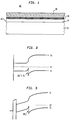
- CCD 10 comprises a substrate body 12 having a surface 14.
- the body 12 is of a semiconductor material, such as single crystalline silicon, which is of either conductivity type, but preferably of p-type.
- a thin layer 16 of a semiconductor material which can be epitaxially grown on the material of the body 12 with good crystalline quality and which has a conduction band and/or valence band different from that of the material of the body 12.
- Such materials include alloys of silicon, such as Si 1-x Ge x , where x is preferably between 0.2 and 0.8, group III-V materials, such as gallium arsenide, aluminum gallium arsenide or the like, and group II-VI materials, such as zinc sulfide.
- group III-V materials such as gallium arsenide, aluminum gallium arsenide or the like
- group II-VI materials such as zinc sulfide.
- the material of the layer 16 is preferably undoped. This difference in the conduction band and/or valence band provides a discontinuity in the conduction band and/or valence band at the interface between the layer 16 and the body 12.
- a thin layer 18 of a dielectric material typically silicon dioxide.
- a dielectric material typically silicon dioxide.
- On the dielectric layer 16 is at least one gate electrode 20.
- the gate electrode 20 is of a conductive arterial, such as a metal or conductive polycrystalline silicon.
- FIG. 2 is a band diagram with no potential applied to the gate electrode 20 of CCD 10 and FIG. 3 is a band diagram with electrode 20 being biased positive.
- the band gap of the alloy is substantially smaller than that of silicon.
- the primary energy gap difference is accounted for by a valence band offset.
- this valence band offset is indicated as Delta Ev.
- the Delta Ev offset provides a well for photogenerated holes to accumulate in.
- this structure has essentially no trapping sites in the region of stored charge because of the high degree of crystalline perfection of the alloy and the interface region. Thus, there is provided a region of potential confinement for photogenerated charge without impurity doping.
- CCD 22 comprises a substrate body 24 of a semiconductor material, such as p-type silicon, having a surface 26.
- a semiconductor material such as p-type silicon
- On the surface 26 is a thin layer 28 of a semiconductor material having a conductance band and/or valence band which is different from that of the material of the body 24.
- a material suitable for the layer 28 is undoped Si 1-x Ge x .
- the semiconductor layer 28 contains a CCD channel region 30 having a field region 32 around it.
- the field region 32 may be formed by highly doping the area of the field region 32 with an n-type conductivity dopant, such as phosphorous, so that the field region 32 is of n+ type conductivity.
- the field region is generally doped at a concentration of 1019 to 1020 impurities/cm3, but can be doped in the range of 1015 to 1021 impurities/cm3.
- the field region 32 which acts as a channel stop, serves to confine stored charges in the CCD channel region 30.
- a thin dielectric layer 34 typically of silicon dioxide.
- a plurality of sets of gate electrodes 36a, 36b, 36c and 36d which extend across the channel region 30 and are in overlapping relation along the channel region 30. Adjacent gate electrodes are insulated from each other by a layer 38 of a dielectric material, such as silicon dioxide.
- the CCD 22 is a four-phase CCD with each set of the gate electrodes 36a, 36b, 36c and 36d being connected to a source of potential, not shown.
- FIG. 6 is a valence band diagram under two of the electrodes 36a and 36b.
- the solid line is for the electrode 36a and the dash line is for the electrode 36b. It can be seen that a well is provided under each of the electrode 36a and 36b so that charges generated under the electrodes 36a and 36b are stored in the well.
- Vm1 is the well potential maximum for the electrode 36a and Vm2 is the well potential maximum for the electrode 36b.
- FIG. 7 is a valance band diagram for the potential in the field region 32 with a positive bias applied thereto.
- the well potential maximum, Vm, in the field region 32 is larger than the well potential maximum of the channel region 30 to ensure confinement of charge during electrode clocking.
- a CCD 10 in which photogenerated charge in the channel region 30 is stored below the surface of the semiconductor layer 16 without doping the semiconductor layer 16. This reduces trapping of the charge so as to improve operation of the CCD at low temperatures.
- antiblooming protection when the charge capacity of the well is exceeded. When excess charge is generated, excess hole photocharge is bloomed into the substrate 12 while photoelectrons are drained away by the field region 32.
- Another advantage of the CCD 10 is that carriers at the interface of the semiconductor layer 28 and dielectric layer 34 can be used during charge integration to suppress interface dark current. Another advantage is that photogenerated charge is not scattered by dopant impurities during read-out of the device. This results in enhanced operating speeds.
- the CCD 22 is shown as a four phase CCD, it can be of any phase.
- the CCD 22 may include more than one channel region 30 as long as the field region 32 extends around all of the channel regions.
- field and/or channel stop technologies other than n+ type conductivity regions may be used.
- a p+ type conductivity region ary be substituted for the n+ type region.
- Control of the potential is the field and channel regions may be achieved by such means as field plates or Schottky barriers.
- the field region may also be achieved by selectively eliminating the semiconductor layer 28 in those regions desired to be a barrier to photo charge transport or by selective deposition of the semiconductor material only in the regions where charge collection and transport are desired.
- the invention may be summarized as follows:
Landscapes
- Solid State Image Pick-Up Elements (AREA)
Applications Claiming Priority (2)
| Application Number | Priority Date | Filing Date | Title |
|---|---|---|---|
| US81921492A | 1992-01-10 | 1992-01-10 | |
| US819214 | 1992-01-10 |
Publications (2)
| Publication Number | Publication Date |
|---|---|
| EP0551140A2 true EP0551140A2 (de) | 1993-07-14 |
| EP0551140A3 EP0551140A3 (en) | 1993-09-15 |
Family
ID=25227506
Family Applications (1)
| Application Number | Title | Priority Date | Filing Date |
|---|---|---|---|
| EP19930100302 Withdrawn EP0551140A3 (en) | 1992-01-10 | 1993-01-11 | Charged coupled device (ccd) having high transfer efficiency at low temperature operation |
Country Status (2)
| Country | Link |
|---|---|
| EP (1) | EP0551140A3 (de) |
| JP (1) | JPH05259196A (de) |
-
1993
- 1993-01-06 JP JP5000687A patent/JPH05259196A/ja active Pending
- 1993-01-11 EP EP19930100302 patent/EP0551140A3/en not_active Withdrawn
Non-Patent Citations (1)
| Title |
|---|
| IBM TECHNICAL DISCLOSURE BULLETIN vol. 19, no. 9, February 1977, NEW YORK US page 3453 G.M. OLESZEK 'HETROJUNCTION BURIED CHARGE-COUPLED DEVICE' * |
Also Published As
| Publication number | Publication date |
|---|---|
| JPH05259196A (ja) | 1993-10-08 |
| EP0551140A3 (en) | 1993-09-15 |
Similar Documents
| Publication | Publication Date | Title |
|---|---|---|
| EP0033876B1 (de) | Halbleitervorrichtung mit drei Anschlussklemmen | |
| US5144398A (en) | Semiconductor device and photoelectric conversion apparatus using the same | |
| US4490573A (en) | Solar cells | |
| JPH0435904B2 (de) | ||
| US5734183A (en) | Heterojunction bipolar transistor structure | |
| US5272357A (en) | Semiconductor device and electronic device by use of the semiconductor | |
| US4550331A (en) | Multilayer modulation doped heterostructure charge coupled device | |
| CA1046638A (en) | Bulk charge coupled device with high doping at buried pn-junction | |
| EP0191201A1 (de) | Halbleiteranordnung mit bidimensionalem Elektronengas | |
| EP0050064A2 (de) | Feldeffekttransistor mit hoher Grenzfrequenz | |
| US4503450A (en) | Accumulation mode bulk channel charge-coupled devices | |
| US5378923A (en) | Semiconductor device including a field effect transistor | |
| US3466512A (en) | Impact avalanche transit time diodes with heterojunction structure | |
| US5241199A (en) | Charge coupled device (CCD) having high transfer efficiency at low temperature operation | |
| EP0551140A2 (de) | Ladungsgekoppelte Anordnung mit hoher Übertragungsleistung bei niedriger Temperatur | |
| EP0437061B1 (de) | Photoelektrischer Umwandler | |
| US5099299A (en) | Modulation doped base heterojunction bipolar transistor | |
| JPH05335615A (ja) | 光電変換装置 | |
| US6037615A (en) | Metal semiconductor FET having doped A1GaAs layer between channel layer and A1GaAs buffer layer | |
| JPH0763090B2 (ja) | 固体撮像装置 | |
| EP0247667B1 (de) | Transistoren mit heissen Ladungsträgern | |
| JP2703885B2 (ja) | 半導体装置 | |
| EP0431835B1 (de) | Bipolares Halbleiterbauelement | |
| US6320211B1 (en) | Semiconductor device and electronic device by use of the semiconductor | |
| US4811070A (en) | Heterojunction bipolar transistor with inversion layer base |
Legal Events
| Date | Code | Title | Description |
|---|---|---|---|
| PUAI | Public reference made under article 153(3) epc to a published international application that has entered the european phase |
Free format text: ORIGINAL CODE: 0009012 |
|
| AK | Designated contracting states |
Kind code of ref document: A2 Designated state(s): DE FR GB |
|
| PUAL | Search report despatched |
Free format text: ORIGINAL CODE: 0009013 |
|
| AK | Designated contracting states |
Kind code of ref document: A3 Designated state(s): DE FR GB |
|
| STAA | Information on the status of an ep patent application or granted ep patent |
Free format text: STATUS: THE APPLICATION IS DEEMED TO BE WITHDRAWN |
|
| 18D | Application deemed to be withdrawn |
Effective date: 19940316 |