EP0549568B1 - Dual contact set for chip card reader - Google Patents
Dual contact set for chip card reader Download PDFInfo
- Publication number
- EP0549568B1 EP0549568B1 EP93103872A EP93103872A EP0549568B1 EP 0549568 B1 EP0549568 B1 EP 0549568B1 EP 93103872 A EP93103872 A EP 93103872A EP 93103872 A EP93103872 A EP 93103872A EP 0549568 B1 EP0549568 B1 EP 0549568B1
- Authority
- EP
- European Patent Office
- Prior art keywords
- card
- contact elements
- contacts
- contact
- chip
- Prior art date
- Legal status (The legal status is an assumption and is not a legal conclusion. Google has not performed a legal analysis and makes no representation as to the accuracy of the status listed.)
- Expired - Lifetime
Links
Images

Classifications
-
- G—PHYSICS
- G06—COMPUTING OR CALCULATING; COUNTING
- G06K—GRAPHICAL DATA READING; PRESENTATION OF DATA; RECORD CARRIERS; HANDLING RECORD CARRIERS
- G06K7/00—Methods or arrangements for sensing record carriers, e.g. for reading patterns
- G06K7/0013—Methods or arrangements for sensing record carriers, e.g. for reading patterns by galvanic contacts, e.g. card connectors for ISO-7816 compliant smart cards or memory cards, e.g. SD card readers
- G06K7/0021—Methods or arrangements for sensing record carriers, e.g. for reading patterns by galvanic contacts, e.g. card connectors for ISO-7816 compliant smart cards or memory cards, e.g. SD card readers for reading/sensing record carriers having surface contacts
-
- H—ELECTRICITY
- H01—ELECTRIC ELEMENTS
- H01R—ELECTRICALLY-CONDUCTIVE CONNECTIONS; STRUCTURAL ASSOCIATIONS OF A PLURALITY OF MUTUALLY-INSULATED ELECTRICAL CONNECTING ELEMENTS; COUPLING DEVICES; CURRENT COLLECTORS
- H01R12/00—Structural associations of a plurality of mutually-insulated electrical connecting elements, specially adapted for printed circuits, e.g. printed circuit boards [PCB], flat or ribbon cables, or like generally planar structures, e.g. terminal strips, terminal blocks; Coupling devices specially adapted for printed circuits, flat or ribbon cables, or like generally planar structures; Terminals specially adapted for contact with, or insertion into, printed circuits, flat or ribbon cables, or like generally planar structures
- H01R12/50—Fixed connections
- H01R12/59—Fixed connections for flexible printed circuits, flat or ribbon cables or like structures
-
- H—ELECTRICITY
- H01—ELECTRIC ELEMENTS
- H01R—ELECTRICALLY-CONDUCTIVE CONNECTIONS; STRUCTURAL ASSOCIATIONS OF A PLURALITY OF MUTUALLY-INSULATED ELECTRICAL CONNECTING ELEMENTS; COUPLING DEVICES; CURRENT COLLECTORS
- H01R12/00—Structural associations of a plurality of mutually-insulated electrical connecting elements, specially adapted for printed circuits, e.g. printed circuit boards [PCB], flat or ribbon cables, or like generally planar structures, e.g. terminal strips, terminal blocks; Coupling devices specially adapted for printed circuits, flat or ribbon cables, or like generally planar structures; Terminals specially adapted for contact with, or insertion into, printed circuits, flat or ribbon cables, or like generally planar structures
- H01R12/70—Coupling devices
- H01R12/71—Coupling devices for rigid printing circuits or like structures
- H01R12/712—Coupling devices for rigid printing circuits or like structures co-operating with the surface of the printed circuit or with a coupling device exclusively provided on the surface of the printed circuit
- H01R12/714—Coupling devices for rigid printing circuits or like structures co-operating with the surface of the printed circuit or with a coupling device exclusively provided on the surface of the printed circuit with contacts abutting directly the printed circuit; Button contacts therefore provided on the printed circuit
-
- H—ELECTRICITY
- H01—ELECTRIC ELEMENTS
- H01R—ELECTRICALLY-CONDUCTIVE CONNECTIONS; STRUCTURAL ASSOCIATIONS OF A PLURALITY OF MUTUALLY-INSULATED ELECTRICAL CONNECTING ELEMENTS; COUPLING DEVICES; CURRENT COLLECTORS
- H01R12/00—Structural associations of a plurality of mutually-insulated electrical connecting elements, specially adapted for printed circuits, e.g. printed circuit boards [PCB], flat or ribbon cables, or like generally planar structures, e.g. terminal strips, terminal blocks; Coupling devices specially adapted for printed circuits, flat or ribbon cables, or like generally planar structures; Terminals specially adapted for contact with, or insertion into, printed circuits, flat or ribbon cables, or like generally planar structures
- H01R12/70—Coupling devices
- H01R12/71—Coupling devices for rigid printing circuits or like structures
- H01R12/72—Coupling devices for rigid printing circuits or like structures coupling with the edge of the rigid printed circuits or like structures
- H01R12/73—Coupling devices for rigid printing circuits or like structures coupling with the edge of the rigid printed circuits or like structures connecting to other rigid printed circuits or like structures
-
- H—ELECTRICITY
- H01—ELECTRIC ELEMENTS
- H01R—ELECTRICALLY-CONDUCTIVE CONNECTIONS; STRUCTURAL ASSOCIATIONS OF A PLURALITY OF MUTUALLY-INSULATED ELECTRICAL CONNECTING ELEMENTS; COUPLING DEVICES; CURRENT COLLECTORS
- H01R12/00—Structural associations of a plurality of mutually-insulated electrical connecting elements, specially adapted for printed circuits, e.g. printed circuit boards [PCB], flat or ribbon cables, or like generally planar structures, e.g. terminal strips, terminal blocks; Coupling devices specially adapted for printed circuits, flat or ribbon cables, or like generally planar structures; Terminals specially adapted for contact with, or insertion into, printed circuits, flat or ribbon cables, or like generally planar structures
- H01R12/50—Fixed connections
- H01R12/59—Fixed connections for flexible printed circuits, flat or ribbon cables or like structures
- H01R12/65—Fixed connections for flexible printed circuits, flat or ribbon cables or like structures characterised by the terminal
- H01R12/67—Fixed connections for flexible printed circuits, flat or ribbon cables or like structures characterised by the terminal insulation penetrating terminals
- H01R12/675—Fixed connections for flexible printed circuits, flat or ribbon cables or like structures characterised by the terminal insulation penetrating terminals with contacts having at least a slotted plate for penetration of cable insulation, e.g. insulation displacement contacts for round conductor flat cables
Definitions
- the invention relates to a contacting apparatus for chip-cards of different types, i.e., chip-cards with contacts being arranged in different arrays and locations on the card.
- a contacting apparatus for a chip-card wherein a set of contact elements is used which comprises a plurality of contact elements, so as to provide for a contact or termination with the card contacts which are placed on the upper surface of a chip-card.
- Each of the contact elements of the set of contact elements comprises one end which is adapted for contacting one of the card contacts.
- the other end of each of said contact elements of the set of contact elements is used for providing the connection to an electronic card processing means for processing the data stored in the chip-card. It is known to either move the card towards the contact elements of the set of contact elements, so as to provide the desired contacting operation, or else it is also possible to move the contact elements towards the card, so as to provide the contacting operation with the card contacts.
- the card contacts are located at a different location on the upper surface of the card compared with the location of the card contacts of a standard chip-card presently used in Germany.
- the known contact apparatus can be used only for one type of chip-card.
- chip-card contacting apparatus which can be used for two types of chip-cards, specifically for chip-cards of the French standard card type and for chip-cards of the German standard card type.
- a contacting apparatus which is useful for two types of chip-cards may be referred to as a dual-contacting apparatus.
- the termination members of the first and second group of contact elements are in the form of insulation displacement contacts and the coupling means comprises a flat cable.
- the cable may be folded to provide the necessary connections.
- the invention provides two possibilities for achieving the above objects.
- a flat cable having 16 leads or wires is used, i.e., all card contacts are individually contacted and have a respective wire assigned thereto.
- the information is supplied in parallel.
- additional contact elements in the set of contact elements.
- Such additional contact elements are used for special purposes, for instance for providing a display indicating that the end or reading position is reached by the chip-card in the contacting apparatus.
- each chip-card comprises 8 card contacts
- the 8 wire flat cable will first provide the termination for a first group of card contacts, i.e. a group comprising all card contacts of the card of a first type (for instance the French card).
- the 8 wire flat cable is twice folded in such a manner that now a second group of card contacts may be terminated.
- the second group of card contacts comprises all card contacts of the card of the second type (for instance the German card). The folding occurs in such a manner that each card contact of the first group which corresponds to an appropriate card contact of the second group is connected with each other by the same wire of the flat cable.
- the double-folding occurs with an angle of 45°, so that a triangular area is formed within which the flat cable is bonded to each other by means of an adhesive, so that an arrangement is obtained which requires little space.
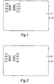
- Figure 1 is a plan view of a first type of a chip-card.
- Figure 2 is a plan view of a second type of a chip-card.
- Figure 3 is a schematic side-elevational view of a contacting apparatus for chip-cards of the two types with the contacting apparatus being shown in its insert and output position for the chip-card.
- Figure 4 is a view similar to Figure 3 with the contacting apparatus and the chip-card being in the reading position.
- Figure 5 is a schematic plan view of the contacting apparatus of Figure 4 with the flat cable being shown in a schematic representation
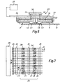
- Figure 6 is a partial sectional view along line 6 in Figure 5.
- Figure 7 represents a first principal possibility for the termination of the chip-card contacts of a chip-card of the first and of the second type.
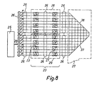
- Figure 8 is a second principal possibility for the termination of the contacts of chip-cards of the first and second type.
- a contacting apparatus shown in Figures 3 to 5 will be discussed, the contacting apparatus being adapted to provide contact with chip-cards of different types, specifically chip-cards of the type shown in Figures 1 and 2.
- the connection between the contacting apparatus, and consequently the connection with the card contacts provided on the chip-cards, for instance with an electronic card processing means is preferably provided by means of a flat cable.
- a preferred means of termination for the flat cable will be discussed in some detail in connection with Figures 7 and 8.
- Figure 1 discloses a chip-card 10 of a first type. Inasmuch as such a chip-card is frequently used in France, it will be referred to simply as "French card”.
- the French card 10 comprises at its upper surface 13 an array of card contacts comprising two vertical rows with card contacts C11, C21, C31, C41 (right row) and C51, C61, C71 and C81 (left row).
- the card contacts on the French card will be referred to as the "French card contacts”.
- Figure 2 discloses a chip-card 12 of a second type which is frequently used in Germany.
- the chip-card will be referred to as the "German card”.
- the German card 12 carries at its upper surface 14 eight (German) card contacts, i.e. C8, C7, C6, C5 (right row) and C4, C3, C2, C1 (left row). If one contemplates an arrangement of the French and German cards above each other, all card contacts of the two cards would define an arrangement which will be called a termination image and which will be discussed later in connection with Figures 7 and 8.
- a dual-contacting apparatus 20 is shown in Figures 3-5 as comprising a housing 22.
- the dual-contacting apparatus 20 can be used either for contacting (or terminating) a French card 10 or a German card 12.
- Figure 3 discloses the insertion of a French card 10 into the contacting apparatus 20.
- a set 23 of contact elements which has to be connected with the card contacts is in its rest position .
- Figure 4 shows the dual-contacting apparatus 20 with the French card 10 being completely inserted.
- the card 10 is now in its reading position.
- the set 23 of contact elements is now in its contacting or termination position, a condition which is shown in detail in Figure 6.
- the card contacts are connected by means of a flat cable 24 with an electronic card processing means 25, i.e., a means for processing the data received from the card.
- a pressure member is referred to by reference numeral 36 and serves for the termination of the flat cable 24 with insulation displacement means described below.
- Figure 5 the flat cable 24 is only shown in a sectional representation, i.e., not in the manner as was shown in Figures 3 and 4. Moreover, Figure 3 permits viewing through the pressure member 36.
- the location of the French as well as of the German card contacts can be realized in this position of a French and German card, respectively. It should be noted that always either one type or the other type is inserted into the dual-contacting apparatus. As can be recognized, the distance or pitch between the card-contacts is the same for the German as well as for the French card contacts.
- Figure 6 discloses in a schematic manner the set 23 of contact elements of the invention.
- the set 23 of contact elements comprises a holding member 32, on the upper surface 33 of which the flat cable 24 may be arranged.
- An insulating body 35 supports a plurality of contact elements, two of which are shown in Figure 6, i.e., contact elements 3 and 6.
- contact elements 3 and 6 In accordance with this invention for each card contact one contact element may be provided.
- additional contact elements for example if different functions are envisaged. For instance, one of such additional contact elements may be used as a "card end switch", i.e. a switch which indicates that the chip-card has reached its end or fully inserted position.
- each contact element 3, 6 is provided with an appropriate insulation displacement means I3, I6. In this way a connection can be provided to a flat cable 24 in a simple manner.
- a German card 12 is shown in its reading position in which the contact element 3 contacts a card contact C3 and contact element 6 contacts a card contact C6.
- FIG 7 shows in an extremely schematic manner the above-mentioned first possibility according to which the French card contacts C11, C21 and so on and the German card contacts C1, C2 and so on are connected via the flat cable 24 having 16 wires with the electronic card processing means 25.
- the flat cable 24 is shown initially as a heavy line and is shown then in a sectional view. Thereupon, on the right-hand side the flat cable 24 is represented by lines representing the wires of the flat cable. Three of such wires are referred to by a, b, and c.
- the elliptic enclosures of the lines representing wires are supposed to indicate that the flat cable extends first to the first or left French/German row of card contacts and thereupon to the second (or right) French/German row of card contacts. Thereupon the flat cable ends to the right of the second row of card contacts.
- one wire of the flat cable 24 is assigned to each individual card contact.
- the card contacts are lead out of the set 23 of contact elements in a parallel manner.
- each one contact element is assigned to each one card contact (see Figure 6), and that each of the contact elements comprises an insulation displacement means.
- the insulation displacement means is shown in Figure 7 (and also in Figure 8) and is each represented by a small cross. This means, at the location of the cross one wire of the flat cable 24 is connected with the corresponding contact element, and the contact element, in turn, can contact the card contact.
- insulation displacement means I3 is assigned to the card contact C3, and the insulation displacement means I3 connects the wire "m” with the contact element 3.
- the wire “n” by-passes the insulation displacement means I3 and is only connected to an insulation displacement means I7.
- the insulation displacement means I7 is provided for and mounted to a contact element not shown (such contact element might be referred to for instance with reference numeral 7) and is adapted for contacting the card contact C7.
- Figure 8 shows in a schematic representation similar to Figure 7 the above-mentioned second possibility for providing a connection between the contact elements and the electronic card processing means 25.
- a flat cable 26 is used which comprises only half the number of wires compared with the flat cable used in the embodiment of Figure 7.
- a flat cable 26 having 8 wires is used.
- This flat cable 26 extends from the electronic card processing means 25, or any other suitable apparatus, to the set 23 of contact elements.
- the set 23 of contact elements shown in Figure 8 is of the same design as the set of contact elements shown in Figure 7.
- an appropriate "French" and "German” contact element is assigned, having an appropriate French and German insulation displacement means.
- the German card contact C3 comprises a corresponding German contact element 3 (see Figure 6), which in turn comprises a German insulation displacement means I3.
- the insulation displacement means I3 connects the wire "m” with the contact element 3.
- the wire "n” by-passes the insulation displacement means I3, i.e. does not contact the insulation displacement means I7 which belongs to the contact element which corresponds to card contact C7.
- German card contact C1 corresponds to the French card contact C11
- German card contact C2 corresponds to the French card contact C21
- C3 corresponds to C61
- C7 corresponds to C71
- C8 corresponds eventually to C81.
- a flat cable 26 with only eight (i-p) wires is used.
- a contact element connection 27 has to be provided so as to connect the wires i-p of the German card contacts with the French card contacts (their corresponding contact elements, respectively).
- this contact element connection 27 is created simply by using a flat cable which leads from the German group of contact elements (contact group 29) to the French group 28 of contact elements (as is shown); or, the flat cable leads from the French group 28 of contact elements to the German group 29 of contact elements in such a manner that the wires of the flat cable 26 serve one contact element in the group of German contact elements and the corresponding contact element in the group of French group of contact elements.
- the flat cable 26 coming from the row of contact elements C5 to C6 is folded over along a line 37 upwardly (or downwardly) and thereupon again but this time (at 38) downwardly (or upwardly), such that the flat cable 26 in the area of the French card contacts (or the corresponding insulation displacement means) extends just opposite to the extension in the area of the German card contacts.
- This is shown in Figure 8 by the corresponding reference to wires i-p.
- wire m which is connected to the insulation displacement means I3 of the card contact C3.
- wire m is connected with the insulation displacement means of the corresponding French card contact C31. This is true in a similar manner for all the other wires of the flat cable 26.
- FIG 8 the folding of the flat cable 26 is shown beginning with the card contacts C5 to C8.
- the folding occurs initially in an upward direction (line 37) and thereupon in a downward (line 38) direction.
- the folding may be carried out first downwardly and then upwardly.
- the flat cable 26 is adhesively bonded to itself in the area of the substantially triangular area of overlap which is formed. In this way a flat design is possible.
- Figure 8 shows that the flat cable 26 starts from the electronic processing means 25 and is initially contacted to the German group of contact elements and thereupon to the French group of contact elements.
- the flat cable ends after leaving the area of the French row of contact elements C51, C61, C71 and C81.
- the flat cable could first be introduced into the French group 28 of contact elements and would then be folded in the manner pointed out above, whereupon the flat cable would enter the group 29 of German contact elements and the cable would end after the insulation displacement means which are assigned to the German card contacts C1-C4 are contacted or terminated.
- contact elements of the same design as shown for contact elements 3, 6 can be used for all the card contacts, i.e., the French and the German contacts. This leads to a simple and cost efficient design.
- connection of an eight-wire flat cable (26) only with one of the group of contact elements, for instance, with the German group of contact elements.
- the respective other group of contact elements, for instance, the French group of contact elements could then be connected with the German group of contact elements in a different manner, for instance by means of a printed circuit or a similar connecting means.
- the corresponding contact elements of the French group of contact elements could be fixedly wired with the corresponding contact elements of the German group of contact elements such that only the connection of the German group (29) of contact elements with the electronic card processing means would be required.
- the contact portions (42) of the contact elements (3, 6) are provided in the form of contact springs, and that the contact springs (42) are arranged in accordance with the ISO standard for the German card contacts and in accordance with the CP8 card system for the French card contacts. Attention is drawn to the fact that the French as well as the German contact portions (42) are arranged with the same distance (pitch) corresponding to the appropriate card contacts.
- the dual-contacting apparatus is designed such that only the only or the other card can be inserted, the housing (22) of the contacting apparatus (20) only comprises a single card insert opening.
- insulation displacement means In the above description, reference has been made to insulation displacement means.
- such means is in the form of insulation displacement contacts of conventional design which pierce and displace the insulation surrounding each conductor and electrically contact with such conductor.
Landscapes
- Engineering & Computer Science (AREA)
- Artificial Intelligence (AREA)
- Computer Vision & Pattern Recognition (AREA)
- Physics & Mathematics (AREA)
- General Physics & Mathematics (AREA)
- Theoretical Computer Science (AREA)
- Coupling Device And Connection With Printed Circuit (AREA)
- Multi-Conductor Connections (AREA)
Description
- The invention relates to a contacting apparatus for chip-cards of different types, i.e., chip-cards with contacts being arranged in different arrays and locations on the card.
- A contacting apparatus for a chip-card is already known wherein a set of contact elements is used which comprises a plurality of contact elements, so as to provide for a contact or termination with the card contacts which are placed on the upper surface of a chip-card. Each of the contact elements of the set of contact elements comprises one end which is adapted for contacting one of the card contacts. The other end of each of said contact elements of the set of contact elements is used for providing the connection to an electronic card processing means for processing the data stored in the chip-card. It is known to either move the card towards the contact elements of the set of contact elements, so as to provide the desired contacting operation, or else it is also possible to move the contact elements towards the card, so as to provide the contacting operation with the card contacts.
- Specifically, reference is made to the prior art as represented by U.S. patent 4,449,775, and German applications DE-OS 32 35 654 and DE-OS 34 33 316.
- As it turns out, different types of chip-cards are used in practice. For the standard chip-card presently used in France, the card contacts are located at a different location on the upper surface of the card compared with the location of the card contacts of a standard chip-card presently used in Germany. The known contact apparatus can be used only for one type of chip-card.
- It would be desirable to provide a contacting apparatus for chip-cards such that it may be used in connection with chip-cards of different types.
- It would also be desirable to provide a chip-card contacting apparatus which can be used for two types of chip-cards, specifically for chip-cards of the French standard card type and for chip-cards of the German standard card type.
- A contacting apparatus which is useful for two types of chip-cards may be referred to as a dual-contacting apparatus.
- In accordance with this invention, there is provided a dual-contacting apparatus as set forth in claim 1.
- Preferred embodiments of the invention are disclosed in the dependent claims.
- Preferably, the termination members of the first and second group of contact elements are in the form of insulation displacement contacts and the coupling means comprises a flat cable. The cable may be folded to provide the necessary connections.
- The invention provides two possibilities for achieving the above objects.
- In accordance with a first possibility for each of the eight card contacts provided on the French as well as on the German card, a flat cable having 16 leads or wires is used, i.e., all card contacts are individually contacted and have a respective wire assigned thereto. At the free end of the cable, i.e. the end of the cable which leads to the electronic card processing means, the information is supplied in parallel.
- It is also possible to use instead of one flat cable having 16 wires, two cables each having 8 wires. Moreover, it is possible to use a cable with more or less wires depending on the number of card contacts to be contacted.
- It is conceivable to provide additional contact elements in the set of contact elements. Such additional contact elements are used for special purposes, for instance for providing a display indicating that the end or reading position is reached by the chip-card in the contacting apparatus.
- Besides providing a parallel arrangement of the card contacts another possibility provided by the invention is a so-called series arrangement of the card contacts. Assuming again that each chip-card comprises 8 card contacts, it will now be sufficient to use just one flat cable having 8 wires. The 8 wire flat cable will first provide the termination for a first group of card contacts, i.e. a group comprising all card contacts of the card of a first type (for instance the French card). Thereupon, the 8 wire flat cable is twice folded in such a manner that now a second group of card contacts may be terminated. The second group of card contacts comprises all card contacts of the card of the second type (for instance the German card). The folding occurs in such a manner that each card contact of the first group which corresponds to an appropriate card contact of the second group is connected with each other by the same wire of the flat cable.
- In accordance with a preferred embodiment of the invention the double-folding occurs with an angle of 45°, so that a triangular area is formed within which the flat cable is bonded to each other by means of an adhesive, so that an arrangement is obtained which requires little space.
- Figure 1 is a plan view of a first type of a chip-card.
- Figure 2 is a plan view of a second type of a chip-card.
- Figure 3 is a schematic side-elevational view of a contacting apparatus for chip-cards of the two types with the contacting apparatus being shown in its insert and output position for the chip-card.
- Figure 4 is a view similar to Figure 3 with the contacting apparatus and the chip-card being in the reading position.
- Figure 5 is a schematic plan view of the contacting apparatus of Figure 4 with the flat cable being shown in a schematic representation,
- Figure 6 is a partial sectional view along
line 6 in Figure 5. - Figure 7 represents a first principal possibility for the termination of the chip-card contacts of a chip-card of the first and of the second type.
- Figure 8 is a second principal possibility for the termination of the contacts of chip-cards of the first and second type.
- In connection with Figures 1 and 2 two different types of chip-cards will be described. Thereupon, a contacting apparatus shown in Figures 3 to 5 will be discussed, the contacting apparatus being adapted to provide contact with chip-cards of different types, specifically chip-cards of the type shown in Figures 1 and 2. The connection between the contacting apparatus, and consequently the connection with the card contacts provided on the chip-cards, for instance with an electronic card processing means is preferably provided by means of a flat cable. A preferred means of termination for the flat cable will be discussed in some detail in connection with Figures 7 and 8.
- Figure 1 discloses a chip-
card 10 of a first type. Inasmuch as such a chip-card is frequently used in France, it will be referred to simply as "French card". TheFrench card 10 comprises at itsupper surface 13 an array of card contacts comprising two vertical rows with card contacts C11, C21, C31, C41 (right row) and C51, C61, C71 and C81 (left row). The card contacts on the French card will be referred to as the "French card contacts". - Figure 2 discloses a chip-
card 12 of a second type which is frequently used in Germany. The chip-card will be referred to as the "German card". TheGerman card 12 carries at itsupper surface 14 eight (German) card contacts, i.e. C8, C7, C6, C5 (right row) and C4, C3, C2, C1 (left row). If one contemplates an arrangement of the French and German cards above each other, all card contacts of the two cards would define an arrangement which will be called a termination image and which will be discussed later in connection with Figures 7 and 8. - A dual-contacting
apparatus 20 is shown in Figures 3-5 as comprising ahousing 22. The dual-contactingapparatus 20 can be used either for contacting (or terminating) aFrench card 10 or aGerman card 12. Figure 3 discloses the insertion of aFrench card 10 into the contactingapparatus 20. Aset 23 of contact elements which has to be connected with the card contacts is in its rest position . Figure 4 shows the dual-contactingapparatus 20 with theFrench card 10 being completely inserted. Thecard 10 is now in its reading position. Also, theset 23 of contact elements is now in its contacting or termination position, a condition which is shown in detail in Figure 6. In the contacting position the card contacts are connected by means of aflat cable 24 with an electronic card processing means 25, i.e., a means for processing the data received from the card. - In Figures 3-6 a pressure member is referred to by
reference numeral 36 and serves for the termination of theflat cable 24 with insulation displacement means described below. - Reference is now made to the extremely schematic plan view of Figure 5. In Figure 5 the
flat cable 24 is only shown in a sectional representation, i.e., not in the manner as was shown in Figures 3 and 4. Moreover, Figure 3 permits viewing through thepressure member 36. The location of the French as well as of the German card contacts can be realized in this position of a French and German card, respectively. It should be noted that always either one type or the other type is inserted into the dual-contacting apparatus. As can be recognized, the distance or pitch between the card-contacts is the same for the German as well as for the French card contacts. - Figure 6 discloses in a schematic manner the
set 23 of contact elements of the invention. Theset 23 of contact elements comprises a holdingmember 32, on theupper surface 33 of which theflat cable 24 may be arranged. An insulatingbody 35 supports a plurality of contact elements, two of which are shown in Figure 6, i.e.,contact elements - Figure 6 also discloses that each
contact element flat cable 24 in a simple manner. In Figure 6 aGerman card 12 is shown in its reading position in which thecontact element 3 contacts a card contact C3 andcontact element 6 contacts a card contact C6. - The use of a
flat cable 24 together with insulation displacement means I3, I6 for all thecontact elements - Figure 7 shows in an extremely schematic manner the above-mentioned first possibility according to which the French card contacts C11, C21 and so on and the German card contacts C1, C2 and so on are connected via the
flat cable 24 having 16 wires with the electronic card processing means 25. - Inasmuch as Figure 7 is only a schematic representation, it should be considered in connection with Figure 6, with the following comments being kept in mind. The
flat cable 24 is shown initially as a heavy line and is shown then in a sectional view. Thereupon, on the right-hand side theflat cable 24 is represented by lines representing the wires of the flat cable. Three of such wires are referred to by a, b, and c. The elliptic enclosures of the lines representing wires are supposed to indicate that the flat cable extends first to the first or left French/German row of card contacts and thereupon to the second (or right) French/German row of card contacts. Thereupon the flat cable ends to the right of the second row of card contacts. - It can be recognized that one wire of the
flat cable 24 is assigned to each individual card contact. Thus, the card contacts are lead out of theset 23 of contact elements in a parallel manner. - It should be emphasized that each one contact element is assigned to each one card contact (see Figure 6), and that each of the contact elements comprises an insulation displacement means. The insulation displacement means is shown in Figure 7 (and also in Figure 8) and is each represented by a small cross. This means, at the location of the cross one wire of the
flat cable 24 is connected with the corresponding contact element, and the contact element, in turn, can contact the card contact. - For instance, insulation displacement means I3 is assigned to the card contact C3, and the insulation displacement means I3 connects the wire "m" with the
contact element 3. The wire "n" by-passes the insulation displacement means I3 and is only connected to an insulation displacement means I7. The insulation displacement means I7 is provided for and mounted to a contact element not shown (such contact element might be referred to for instance with reference numeral 7) and is adapted for contacting the card contact C7. - In Figure 7 some additional insulation displacement means are shown, i.e., the insulation displacement means I81, I41, and I6. Similar comments will be true for all card contacts and the corresponding contact elements of the set of contact elements, and also for the insulation displacement means of the contact elements.
- Figure 8 shows in a schematic representation similar to Figure 7 the above-mentioned second possibility for providing a connection between the contact elements and the electronic card processing means 25. According to Figure 8 a
flat cable 26 is used which comprises only half the number of wires compared with the flat cable used in the embodiment of Figure 7. Specifically, aflat cable 26 having 8 wires is used. Thisflat cable 26 extends from the electronic card processing means 25, or any other suitable apparatus, to theset 23 of contact elements. Theset 23 of contact elements shown in Figure 8 is of the same design as the set of contact elements shown in Figure 7. Thus, to each French card contact as well as each German card contact an appropriate "French" and "German" contact element is assigned, having an appropriate French and German insulation displacement means. Moreover, aFrench group 28 of contact elements and aGerman group 29 of contact elements is formed. Insofar attention is drawn to the reference numerals of Figure 7. For instance, the German card contact C3 comprises a corresponding German contact element 3 (see Figure 6), which in turn comprises a German insulation displacement means I3. The insulation displacement means I3 connects the wire "m" with thecontact element 3. The wire "n" by-passes the insulation displacement means I3, i.e. does not contact the insulation displacement means I7 which belongs to the contact element which corresponds to card contact C7. - Between the French card contacts and the German card contacts a "twice mirrored image or back-to-back" relation exists. This means, the German card contact C1 corresponds to the French card contact C11, German card contact C2 corresponds to the French card contact C21, C3 corresponds to C61, C7 corresponds to C71, and C8 corresponds eventually to C81.
- In accordance with the invention a
flat cable 26 with only eight (i-p) wires is used. To make this possible acontact element connection 27 has to be provided so as to connect the wires i-p of the German card contacts with the French card contacts (their corresponding contact elements, respectively). - In accordance with the invention this
contact element connection 27 is created simply by using a flat cable which leads from the German group of contact elements (contact group 29) to theFrench group 28 of contact elements (as is shown); or, the flat cable leads from theFrench group 28 of contact elements to theGerman group 29 of contact elements in such a manner that the wires of theflat cable 26 serve one contact element in the group of German contact elements and the corresponding contact element in the group of French group of contact elements. - In accordance with the invention the
flat cable 26 coming from the row of contact elements C5 to C6 is folded over along aline 37 upwardly (or downwardly) and thereupon again but this time (at 38) downwardly (or upwardly), such that theflat cable 26 in the area of the French card contacts (or the corresponding insulation displacement means) extends just opposite to the extension in the area of the German card contacts. This is shown in Figure 8 by the corresponding reference to wires i-p. Consider for instance wire m which is connected to the insulation displacement means I3 of the card contact C3. One recognizes that, in fact, the same wire m is connected with the insulation displacement means of the corresponding French card contact C31. This is true in a similar manner for all the other wires of theflat cable 26. - In Figure 8 the folding of the
flat cable 26 is shown beginning with the card contacts C5 to C8. The folding occurs initially in an upward direction (line 37) and thereupon in a downward (line 38) direction. As mentioned above, the folding may be carried out first downwardly and then upwardly. - Preferably, the
flat cable 26 is adhesively bonded to itself in the area of the substantially triangular area of overlap which is formed. In this way a flat design is possible. - It should be noted that the representation of Figure 8 shows that the
flat cable 26 starts from the electronic processing means 25 and is initially contacted to the German group of contact elements and thereupon to the French group of contact elements. The flat cable ends after leaving the area of the French row of contact elements C51, C61, C71 and C81. It can be readily recognized that a reverse arrangement is possible, i.e., the flat cable could first be introduced into theFrench group 28 of contact elements and would then be folded in the manner pointed out above, whereupon the flat cable would enter thegroup 29 of German contact elements and the cable would end after the insulation displacement means which are assigned to the German card contacts C1-C4 are contacted or terminated. - Due to the arrangement provided by the invention contact elements of the same design as shown for
contact elements - It is also possible to realize the two principal or basic possibilities for connection or termination as shown in Figures 7 and 8 by cables other than a flat cable.
- It is also conceivable to provide a connection of an eight-wire flat cable (26) only with one of the group of contact elements, for instance, with the German group of contact elements. The respective other group of contact elements, for instance, the French group of contact elements could then be connected with the German group of contact elements in a different manner, for instance by means of a printed circuit or a similar connecting means. Moreover, the corresponding contact elements of the French group of contact elements could be fixedly wired with the corresponding contact elements of the German group of contact elements such that only the connection of the German group (29) of contact elements with the electronic card processing means would be required.
- It should further be noted that the contact portions (42) of the contact elements (3, 6) are provided in the form of contact springs, and that the contact springs (42) are arranged in accordance with the ISO standard for the German card contacts and in accordance with the CP8 card system for the French card contacts. Attention is drawn to the fact that the French as well as the German contact portions (42) are arranged with the same distance (pitch) corresponding to the appropriate card contacts. Inasmuch as in accordance with the invention the dual-contacting apparatus is designed such that only the only or the other card can be inserted, the housing (22) of the contacting apparatus (20) only comprises a single card insert opening.
- In the above description, reference has been made to insulation displacement means. In practice, such means is in the form of insulation displacement contacts of conventional design which pierce and displace the insulation surrounding each conductor and electrically contact with such conductor.
Claims (8)
- A dual-contacting apparatus (20) for contacting selectively the card contacts of a chip-card (10) of a first type where the card contacts are arranged in a first array and a first location, or the card contacts of a chip-card (12) of a second type where the card contacts are arranged in a second array and a second location, said apparatus having a set (23) of contact elements which comprises:insulating body means (35),a plurality of contact elements (3, 6) supported by said insulating body means (35), wherein said contact elements (3, 6) form a first group (28) of contact elements which are adapted for contacting the contacts of said chip-card of said first type, and wherein further said contact elements (3, 6) form a second group (29) of contact elements which serve for contacting the card contacts of said chip-card of said second type,means (24, 26) for connecting the contact elements (3, 6) with an electronic card processing means (25), wherein each contact element (3, 6) comprises a termination member (13, 16) adapted for connection with the card processing means (25) and a contact member (42) for contacting one of the card contacts, and said apparatus further comprising a housing, said housing having a single card insert opening for the insertion of either the chip-card of said first type or said second type.
- The apparatus of claim 1, characterized in that the contact members (42) are designed as contact element springs, and the contact element springs (42) are designed in accordance with the ISO standard for the second card contacts and in accordance with the CP8 system for the first card contacts.
- The apparatus of one or more of the preceding claims, characterized in that the contact members (42) of said first and second groups are arranged with the same pitch in accordance with the corresponding card contacts.
- The apparatus of one or more of the preceding claims, characterized in that in the housing (22) a card support is arranged for selectively receiving only a single card, i.e. a card of the first or of the second type, such that a card being located in a reading position either provides for contact of only the first or of only the second group of contact elements (3, 6) with either the group of card contacts of said chip-card of said first type or the group of card contacts of said chip-card of said second type.
- The apparatus as set forth in any of the preceding claims, characterized in that the contact elements of the set (23) of contact elements comprise termination means which are contacted by a flat cable or printed circuit.
- The apparatus of any of the preceding claims, wherein contact elements of the same design are used for all the card contacts, i.e., the French and the German contacts.
- The apparatus of any of the preceding claims, wherein additional contact elements in the set (23) of contact elements are provided and used for special purposes, for instance for providing a display indicating that the end or reading position is reached by the chip-card in the contacting apparatus.
- The apparatus of one or more of the preceding claims, characterized in that the set (23) of contact elements is a separate component which can be inserted into a housing (22) of the contacting apparatus (20).
Applications Claiming Priority (3)
| Application Number | Priority Date | Filing Date | Title |
|---|---|---|---|
| DE3618091 | 1986-05-30 | ||
| DE3618091A DE3618091C1 (en) | 1986-05-30 | 1986-05-30 | |
| EP87106109A EP0247368A1 (en) | 1986-05-30 | 1987-04-28 | Dual contact set for chip card reader |
Related Parent Applications (2)
| Application Number | Title | Priority Date | Filing Date |
|---|---|---|---|
| EP87106109.9 Division | 1987-04-28 | ||
| EP87106109A Division EP0247368A1 (en) | 1986-05-30 | 1987-04-28 | Dual contact set for chip card reader |
Publications (3)
| Publication Number | Publication Date |
|---|---|
| EP0549568A2 EP0549568A2 (en) | 1993-06-30 |
| EP0549568A3 EP0549568A3 (en) | 1993-07-28 |
| EP0549568B1 true EP0549568B1 (en) | 1997-03-19 |
Family
ID=6301875
Family Applications (2)
| Application Number | Title | Priority Date | Filing Date |
|---|---|---|---|
| EP87106109A Withdrawn EP0247368A1 (en) | 1986-05-30 | 1987-04-28 | Dual contact set for chip card reader |
| EP93103872A Expired - Lifetime EP0549568B1 (en) | 1986-05-30 | 1987-04-28 | Dual contact set for chip card reader |
Family Applications Before (1)
| Application Number | Title | Priority Date | Filing Date |
|---|---|---|---|
| EP87106109A Withdrawn EP0247368A1 (en) | 1986-05-30 | 1987-04-28 | Dual contact set for chip card reader |
Country Status (4)
| Country | Link |
|---|---|
| US (1) | US4799891A (en) |
| EP (2) | EP0247368A1 (en) |
| JP (1) | JPS62296382A (en) |
| DE (1) | DE3618091C1 (en) |
Families Citing this family (33)
| Publication number | Priority date | Publication date | Assignee | Title |
|---|---|---|---|---|
| DE3810274C2 (en) * | 1988-03-25 | 2000-05-25 | Amphenol Corp | Chip card contacting device |
| DE8817092U1 (en) * | 1988-03-25 | 1992-11-05 | Amphenol Corp., Wallingford, Conn. | Chip card reader |
| US5225653A (en) * | 1988-11-09 | 1993-07-06 | Societe D'applications Generales D'electricite Et De Mechanique Sagen (Societe Anonyme Francaise) | Chip card receiver |
| FR2638876B1 (en) * | 1988-11-09 | 1992-02-14 | Sagem | CHIP CARD RECEIVER |
| US5369259A (en) * | 1989-09-21 | 1994-11-29 | Amphenol Corporation | Chip card reader |
| DE4118312C2 (en) * | 1991-06-04 | 1995-03-09 | Amphenol Tuchel Elect | Contact set for a card with contact zones |
| FR2679679A1 (en) * | 1991-07-23 | 1993-01-29 | Innovatron Sa | Memory card reader with two mechanical operating positions |
| US5332889A (en) * | 1992-12-18 | 1994-07-26 | Datacard Corporation | Integrated circuit card programming device |
| EP0698247B1 (en) * | 1993-05-14 | 1998-09-02 | AMPHENOL-TUCHEL ELECTRONICS GmbH | Smt reader for sim and standard cards |
| US5726432A (en) * | 1993-05-14 | 1998-03-10 | Amphenol-Tuchel Electronics Gmbh | Contacting system or reader for chip cards |
| FR2726694B1 (en) * | 1994-11-07 | 1996-12-06 | Itt Composants Instr | ELECTRICAL CONNECTOR FOR AN ELECTRONIC MEMORY CARD COMPRISING ELECTRICAL CONNECTION MEANS OF THE INSULATOR DISPLACEMENT TYPE |
| DE19506606C2 (en) * | 1995-02-24 | 1996-12-19 | Amphenol Tuchel Elect | Smart card reader |
| DE19508363C1 (en) * | 1995-03-10 | 1996-07-25 | Amphenol Tuchel Elect | Housing for a chip card |
| DE19516987A1 (en) * | 1995-05-09 | 1996-11-14 | Amphenol Tuchel Elect | Card reading device for chip cards and / or SIM cards with different thickness |
| DE19521721B4 (en) * | 1995-06-14 | 2006-12-07 | Amphenol-Tuchel Electronics Gmbh | Shielded contacting device |
| ES2119688B1 (en) * | 1996-07-03 | 1999-06-01 | Juan Roura Y Cia S A | SUPPORT FOR ELECTRICAL AND ELECTRONIC COMPONENTS. |
| DE19634565C1 (en) * | 1996-08-27 | 1997-11-06 | Amphenol Tuchel Elect | Contact carrier for chip-card reader with automatic SMD components equipping |
| DE19638622A1 (en) * | 1996-09-20 | 1998-03-26 | Amphenol Tuchel Elect | Chip card contacting device |
| EP0840246B2 (en) * | 1996-11-05 | 2011-03-16 | Amphenol-Tuchel Electronics GmbH | Contact device for SIM-cards |
| US6089895A (en) * | 1997-05-21 | 2000-07-18 | Japan Aviation Electronics Industry, Limited | Card connector |
| GB2327792B (en) * | 1997-07-25 | 2001-09-12 | Nokia Mobile Phones Ltd | A data card housing |
| GB2327791B (en) * | 1997-07-25 | 2001-03-21 | Nokia Mobile Phones Ltd | A data card connector |
| US5979771A (en) * | 1997-10-03 | 1999-11-09 | Siemens Information And Communication Networks, Inc. | Apparatus to verify position of electrical contacts within a sliding SIM mechanism |
| JP3295715B2 (en) * | 1997-12-26 | 2002-06-24 | 日本圧着端子製造株式会社 | Printed wiring board connector and method of manufacturing the same |
| NL1008466C2 (en) * | 1998-03-04 | 1999-09-07 | Nedap Nv | Entry card system for public transport and ski resorts etc. |
| US6168077B1 (en) | 1998-10-21 | 2001-01-02 | Litronic, Inc. | Apparatus and method of providing a dual mode card and reader |
| WO2000030018A1 (en) * | 1998-11-12 | 2000-05-25 | International Data Limited Doing Business As Cardtalk Unlimited | Interactive communication system |
| FI107973B (en) | 1999-03-11 | 2001-10-31 | Nokia Mobile Phones Ltd | A method and means for using additional cards in a mobile telephony |
| US6438638B1 (en) | 2000-07-06 | 2002-08-20 | Onspec Electronic, Inc. | Flashtoaster for reading several types of flash-memory cards with or without a PC |
| US7295443B2 (en) | 2000-07-06 | 2007-11-13 | Onspec Electronic, Inc. | Smartconnect universal flash media card adapters |
| DE10206233B4 (en) * | 2002-02-15 | 2005-07-07 | Robert Bosch Gmbh | Communication arrangement and method for information transmission |
| US6860766B2 (en) | 2002-03-08 | 2005-03-01 | Cinch Connectors, Inc. | Electrical connector |
| US7441701B2 (en) | 2004-07-29 | 2008-10-28 | Zih Corp. | Universal card reader apparatus and method |
Family Cites Families (14)
| Publication number | Priority date | Publication date | Assignee | Title |
|---|---|---|---|---|
| US3617706A (en) * | 1969-08-04 | 1971-11-02 | Cred X Corp | Verification system |
| DE2361129A1 (en) * | 1973-12-07 | 1975-06-12 | Siemens Ag | Multiple plug connector for high density equipment - uses flexible track-conductor plate between pins and conductor ends |
| US4009921A (en) * | 1975-07-31 | 1977-03-01 | Thomas & Betts Corporation | Electrical contact and support means therefor |
| DE2613406C3 (en) * | 1976-03-29 | 1980-09-18 | Siemens Ag, 1000 Berlin Und 8000 Muenchen | Process for the production of foil cabling |
| DE2637139C3 (en) * | 1976-08-18 | 1980-08-21 | Siemens Ag, 1000 Berlin Und 8000 Muenchen | Process for the production of foil cabling |
| US4449775A (en) * | 1978-12-27 | 1984-05-22 | Compaganie Internationale Pour L'informatique Cii-Honeywell Bull (Societe Anonyme) | Connector for portable objects such as credit cards |
| US4270826A (en) * | 1979-02-01 | 1981-06-02 | Thomas & Betts Corporation | Zero insertion force connector |
| DE3235654A1 (en) * | 1982-09-27 | 1984-03-29 | Siemens AG, 1000 Berlin und 8000 München | Contacting device for a plug-in card |
| JPS5960522A (en) * | 1982-09-30 | 1984-04-06 | Canon Inc | Electronic apparatus |
| FR2552252B1 (en) * | 1983-09-21 | 1987-07-31 | Dassault Electronique | MIXED READER FOR MAGNETIC TRACK AND / OR ELECTRONIC CHIP CARDS |
| US4724310A (en) * | 1984-07-02 | 1988-02-09 | Tokyo Tatsuno Co., Ltd. | Device for inserting and holding an IC card as an external memory during reading and writing operations |
| DE3442397A1 (en) * | 1984-11-20 | 1986-05-22 | Siemens AG, 1000 Berlin und 8000 München | CHIP CARD READER |
| FR2592193B1 (en) * | 1985-09-20 | 1988-07-22 | Michot Gerard | READER FOR ELECTRONIC INFORMATION MEDIUM |
| DE3645268C2 (en) * | 1986-01-29 | 1996-08-14 | Amphenol Corp | Card holder for a reader for a chip card |
-
1986
- 1986-05-30 DE DE3618091A patent/DE3618091C1/de not_active Expired
-
1987
- 1987-04-28 EP EP87106109A patent/EP0247368A1/en not_active Withdrawn
- 1987-04-28 EP EP93103872A patent/EP0549568B1/en not_active Expired - Lifetime
- 1987-05-11 US US07/048,170 patent/US4799891A/en not_active Expired - Fee Related
- 1987-05-29 JP JP62131902A patent/JPS62296382A/en active Pending
Also Published As
| Publication number | Publication date |
|---|---|
| EP0247368A1 (en) | 1987-12-02 |
| DE3618091C1 (en) | 1987-09-10 |
| US4799891A (en) | 1989-01-24 |
| EP0549568A2 (en) | 1993-06-30 |
| EP0549568A3 (en) | 1993-07-28 |
| JPS62296382A (en) | 1987-12-23 |
Similar Documents
| Publication | Publication Date | Title |
|---|---|---|
| US4799891A (en) | Dual-contacting apparatus for chip-cards | |
| US7719847B2 (en) | Smartconnect flash card adapter | |
| US5399105A (en) | Conductive shroud for electrical connectors | |
| US4893001A (en) | IC card | |
| US5491830A (en) | Automatic slot identification and address decoder arrangement | |
| US6097883A (en) | Dual state memory card having combined and single circuit operation | |
| US5982624A (en) | IC card | |
| NO314477B1 (en) | Coupler with reduced cross section | |
| US5928036A (en) | Dual row memory card connector | |
| CN102891391A (en) | Double stack compact flash card connector | |
| US6585525B2 (en) | Memory modules having conductors at edges thereof and configured to conduct signals to or from the memory modules via the respective edges | |
| US6855001B2 (en) | Modular system | |
| EP0926617B1 (en) | A smart card reader | |
| JPS58201277A (en) | Internal connections for interfaces in data stations | |
| EP1427062B1 (en) | Electric connector | |
| US5636997A (en) | Connection apparatus of circuit board | |
| JP2571021B2 (en) | Connection adapter and mounting structure for semiconductor device | |
| US6551132B1 (en) | Stacked electrical card connector assembly | |
| US20060105592A1 (en) | Memory card structure | |
| US6068515A (en) | Equipment plug connector for a stack of cardshaped data carrier arrangements | |
| US6857906B2 (en) | Connector that occupies minimal cb surface | |
| JPS59161097A (en) | Flat calbe type start connector | |
| JPS63261685A (en) | Multiterminal connector | |
| KR950014725B1 (en) | Rack selection device of plc | |
| JPS6142082A (en) | Talken card reading device |
Legal Events
| Date | Code | Title | Description |
|---|---|---|---|
| PUAI | Public reference made under article 153(3) epc to a published international application that has entered the european phase |
Free format text: ORIGINAL CODE: 0009012 |
|
| PUAL | Search report despatched |
Free format text: ORIGINAL CODE: 0009013 |
|
| 17P | Request for examination filed |
Effective date: 19930310 |
|
| AC | Divisional application: reference to earlier application |
Ref document number: 247368 Country of ref document: EP |
|
| AK | Designated contracting states |
Kind code of ref document: A2 Designated state(s): FR GB IT NL SE |
|
| AK | Designated contracting states |
Kind code of ref document: A3 Designated state(s): FR GB IT NL SE |
|
| 17Q | First examination report despatched |
Effective date: 19950123 |
|
| GRAG | Despatch of communication of intention to grant |
Free format text: ORIGINAL CODE: EPIDOS AGRA |
|
| GRAH | Despatch of communication of intention to grant a patent |
Free format text: ORIGINAL CODE: EPIDOS IGRA |
|
| GRAH | Despatch of communication of intention to grant a patent |
Free format text: ORIGINAL CODE: EPIDOS IGRA |
|
| GRAA | (expected) grant |
Free format text: ORIGINAL CODE: 0009210 |
|
| AC | Divisional application: reference to earlier application |
Ref document number: 247368 Country of ref document: EP |
|
| AK | Designated contracting states |
Kind code of ref document: B1 Designated state(s): FR GB IT NL SE |
|
| PG25 | Lapsed in a contracting state [announced via postgrant information from national office to epo] |
Ref country code: NL Free format text: LAPSE BECAUSE OF FAILURE TO SUBMIT A TRANSLATION OF THE DESCRIPTION OR TO PAY THE FEE WITHIN THE PRESCRIBED TIME-LIMIT Effective date: 19970319 Ref country code: IT Free format text: LAPSE BECAUSE OF FAILURE TO SUBMIT A TRANSLATION OF THE DESCRIPTION OR TO PAY THE FEE WITHIN THE PRE;WARNING: LAPSES OF ITALIAN PATENTS WITH EFFECTIVE DATE BEFORE 2007 MAY HAVE OCCURRED AT ANY TIME BEFORE 2007. THE CORRECT EFFECTIVE DATE MAY BE DIFFERENT FROM THE ONE RECORDED.SCRIBED TIME-LIMIT Effective date: 19970319 Ref country code: FR Effective date: 19970319 |
|
| PG25 | Lapsed in a contracting state [announced via postgrant information from national office to epo] |
Ref country code: SE Effective date: 19970619 Ref country code: GB Free format text: LAPSE BECAUSE OF NON-PAYMENT OF DUE FEES Effective date: 19970619 |
|
| NLV1 | Nl: lapsed or annulled due to failure to fulfill the requirements of art. 29p and 29m of the patents act | ||
| EN | Fr: translation not filed | ||
| PLBE | No opposition filed within time limit |
Free format text: ORIGINAL CODE: 0009261 |
|
| GBPC | Gb: european patent ceased through non-payment of renewal fee |
Effective date: 19970619 |
|
| 26N | No opposition filed |