EP0547850A1 - Buried- type semiconductor laser device - Google Patents
Buried- type semiconductor laser device Download PDFInfo
- Publication number
- EP0547850A1 EP0547850A1 EP92311363A EP92311363A EP0547850A1 EP 0547850 A1 EP0547850 A1 EP 0547850A1 EP 92311363 A EP92311363 A EP 92311363A EP 92311363 A EP92311363 A EP 92311363A EP 0547850 A1 EP0547850 A1 EP 0547850A1
- Authority
- EP
- European Patent Office
- Prior art keywords
- buried
- semiconductor laser
- laser device
- layer
- type semiconductor
- Prior art date
- Legal status (The legal status is an assumption and is not a legal conclusion. Google has not performed a legal analysis and makes no representation as to the accuracy of the status listed.)
- Granted
Links
Images

Classifications
-
- H—ELECTRICITY
- H01—ELECTRIC ELEMENTS
- H01S—DEVICES USING THE PROCESS OF LIGHT AMPLIFICATION BY STIMULATED EMISSION OF RADIATION [LASER] TO AMPLIFY OR GENERATE LIGHT; DEVICES USING STIMULATED EMISSION OF ELECTROMAGNETIC RADIATION IN WAVE RANGES OTHER THAN OPTICAL
- H01S5/00—Semiconductor lasers
- H01S5/20—Structure or shape of the semiconductor body to guide the optical wave ; Confining structures perpendicular to the optical axis, e.g. index or gain guiding, stripe geometry, broad area lasers, gain tailoring, transverse or lateral reflectors, special cladding structures, MQW barrier reflection layers
- H01S5/22—Structure or shape of the semiconductor body to guide the optical wave ; Confining structures perpendicular to the optical axis, e.g. index or gain guiding, stripe geometry, broad area lasers, gain tailoring, transverse or lateral reflectors, special cladding structures, MQW barrier reflection layers having a ridge or stripe structure
- H01S5/227—Buried mesa structure ; Striped active layer
- H01S5/2275—Buried mesa structure ; Striped active layer mesa created by etching
-
- H—ELECTRICITY
- H01—ELECTRIC ELEMENTS
- H01S—DEVICES USING THE PROCESS OF LIGHT AMPLIFICATION BY STIMULATED EMISSION OF RADIATION [LASER] TO AMPLIFY OR GENERATE LIGHT; DEVICES USING STIMULATED EMISSION OF ELECTROMAGNETIC RADIATION IN WAVE RANGES OTHER THAN OPTICAL
- H01S5/00—Semiconductor lasers
- H01S5/30—Structure or shape of the active region; Materials used for the active region
- H01S5/32—Structure or shape of the active region; Materials used for the active region comprising PN junctions, e.g. hetero- or double- heterostructures
- H01S5/323—Structure or shape of the active region; Materials used for the active region comprising PN junctions, e.g. hetero- or double- heterostructures in AIIIBV compounds, e.g. AlGaAs-laser, InP-based laser
- H01S5/3235—Structure or shape of the active region; Materials used for the active region comprising PN junctions, e.g. hetero- or double- heterostructures in AIIIBV compounds, e.g. AlGaAs-laser, InP-based laser emitting light at a wavelength longer than 1000 nm, e.g. InP-based 1300 nm and 1500 nm lasers
- H01S5/32391—Structure or shape of the active region; Materials used for the active region comprising PN junctions, e.g. hetero- or double- heterostructures in AIIIBV compounds, e.g. AlGaAs-laser, InP-based laser emitting light at a wavelength longer than 1000 nm, e.g. InP-based 1300 nm and 1500 nm lasers based on In(Ga)(As)P
Definitions
- This invention relates to an improvement on a buried-type semiconductor laser device to be used as a light source in an optical telecommunication system.
- a semiconductor laser device to be used as a light source in an optical telecommunication system is required to have various functional features such as a high output power and a low threshold current, and a high speed modulation capability.
- a buried-type semiconductor laser device (having a BH structure) is known to meet such requirements.
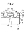
- FIG. 2 of the accompanying drawings illustrates a typical known buried-type semiconductor laser device.
- the buried-type semiconductor laser device 14 comprises an n-InP semiconductor substrate 15, on which an n-InP buffer layer 16, a nondoped GalnAsP active layer 17 (having an energy band gap wavelength of 1.3 ⁇ m), InP clad layers 18 and 19 and a GalnAs contact layer 20 are sequentially formed by means of an epitaxial growth technique such as the MOCVD method to bring forth a multilayer structure.
- p-InP current blocking layers 21 and n-InP current blocking layers 22 extends from the respective upper edges of the clad layer 18 to cover the etched areas of the buffer layer 16 and then grooves 23 are cut through the current blocking layers 21 and 22, the clad layer 19 and the contact layer 20 in order to reduce the device capacity.
- the grooves 23 and part of the segmented contact layer are covered by an Si0 2 insulating film 24.
- a buried-type semiconductor laser device 14 having a configuration as illustrated in Fig. 2 is subject to internal stresses (distortions) particularly in the active layer 17 which is particularly remarkable at high temperature due to the significant difference in the thermal expansion coefficient between and the close physical proximity of the insulating films 24 covering the surface of the grooves 23 and the active layer 17.
- a semiconductor laser device 14 which is subject to such distortions cannot reliably operate for a long period of time.
- a buried-type semiconductor laser device comprising a semiconductor substrate, a first ridge mesa formed on said substrate, said first ridge mesa being covered on the top with at least an active layer and provided at both lateral edges with a current blocking layers of p-n reverse junction semiconductors arranged along the active layer for confining electric currents, and a second ridge mesa formed by said first ridge mesa and said current blocking layers and provided at both lateral edges with a semi- insulating layer.
- Said active layer preferably has a bulk structure, a quantum well structure or a strained quantum well structure.
- Said active layer formed on said first ridge mesa is preferably covered with a clad layer.
- Said second ridge mesa formed by said first ridge mesa and said current blocking layers may additionally comprise clad and contact layers.
- Said current blocking layers may be made of n-InP and p-InP and said semi-insulating layer may be made of Fe doped InP or polyimide and covered with an InP layer.
- a buried-type semiconductor laser device can effectively confine injection currents by its current blocking layers of p-n reverse junction semiconductors and therefore shows a low threshold current for laser oscillation and a reduced capacity of the device due to the arrangement of a semi-insulating layer.
- a buried-type semiconductor laser device does not have grooves in the close proximity of an active layer and insulating films covering the grooves (and having a thermal expansion coefficient different from that of the active layer), it is practically free from internal stresses and distortions even if it is driven at a high temperature.
- a buried-type semiconductor laser device operates stably and reliably for a prolonged period of time, if it is driven at a high temperature.
- FIG. 1 of the accompanying drawings that illustrates a preferred embodiment of the invention.
- the buried-type semiconductor laser device 1 comprises an n-InP semiconductor substrate 2, on which an n-InP buffer layer 3, a nondoped GalnAsP active layer having an energy band gap wavelength of 1.3 f..lm, a p-InP clad layer 5, a p-InP clad layer6, a p-GalnAs contact layer 7, a p-InP current blocking layer 9, an n-InP current blocking layer 10, an n-InP layer 12 and a semi-insulating layer 13 are sequentially formed to bring forth a multilayer structure and is provided with a first ridge mesa 8 and a second ridge mesa 11.
- the semiconductor substrate 2 typically may have a thickness of 350m and the buffer layer 3, the active layer 4 and the clad layer 5 may respectively have thicknesses of 1 ⁇ m, 0.1 ⁇ m and 0.5 ⁇ m, while the clad layer 6, the contact layer 7 and the current blocking layer 9 may respectively have thicknesses of 2 ⁇ m, 0.3 ⁇ m and 2 ⁇ m and the thicknesses of the current blocking layer 10, the n-InP layer 12 and the semi-insulating layer 13 may respectively be 1 ⁇ m, 0.7 ⁇ m and 3 ⁇ m, although the above figures are cited only as examples and the present invention is not limited thereto.
- the semi-insulating layer 13 may alternatively be made of polyimide and, while the active layer 4 of this embodiment has a bulk structure, it may alternatively have a different structure such as a quantum well structure or a strained quantum well structure.
- a semiconductor laser device 1 as described above is subjected to current confinement to be realized by the current blocking layers 9 and 10, involving a p-n reverse junction, it can be driven by a low threshold current and the capacity of the device 1 is reduced by the existence of segmented semi- insulating layer 13 disposed at the lateral sides of the second ridge mesa 11.
- the device 1 maintains its reliability because its active layer 4 is practically free from stress, if the device 1 is used at a high temperature for a prolong period of time.
- the device 1 of the invention does not have any grooves which are covered by an insulating film having a thermal expansion coefficient significantly different from that of the active layer and located in the proximity of the active layer as in the case of a conventional device described above by referring to Fig. 2.
- a buried-type semiconductor laser device 1 according to the invention and illustrated in Fig. 1 can be prepared by way of a manufacturing process as described below.
- a buffer layer 3, an active layer4 and a clad layer 5 are formed on an n-InP semiconductor substrate 2 by a first application of an epitaxial growth technique (MOCVD method).
- MOCVD method an epitaxial growth technique
- the surface of the clad layer 5 is masked along a center line for a width of approximately 1.5 ⁇ m and the layers from the clad layer 5 down to the buffer layer 3 are etched by a first application of a (known) photolithography technique to produce a first ridge mesa 8.
- the surface of the active layer is masked by Si0 2 and a current blocking layer 9 is formed in segments on the areas that have been etched for the first time.
- segments of another current blocking layer 10 are selectively made to grow on the respective segments of the current blocking layer 9 until they reach the height of the surface of the active layer 4.
- a clad layer 6 and a contact layer 7 are sequentially formed on the active layer 4 and the current blocking layer 10 by a second application of an epitaxial growth technique.
- the surface of the contact layer 7 is masked along a center line for a width of approximately 5 to 20 ⁇ m and then the layers from the contact layer 7 down to the buffer layer 3 are etched by a second application of a photolithography technique to produce a second ridge mesa 11.
- a semi-insulating layer 13 and an InP layer 12 are sequentially formed in segments on the second etched areas by means of an epitaxial growth technique to produce a buried-type semiconductor laser device 1.
- the Si0 2 mask is removed from the buried-type semiconductor laser device 1 and p- and n-electrodes are formed.
- the above described sixth step may alternatively be inserted after the third step.
- the semi-insulating layer 13 is made of polyimide, the operation of successively growing layers by means of an epitaxial growth technique will be omitted.
- a buried-type semiconductor laser device operates stably and reliably at a high temperature for a prolonged period of time, because it is free from distortions in its active layer due to stresses that may arise when it is driven at a high temperature.
Abstract
Description
- This invention relates to an improvement on a buried-type semiconductor laser device to be used as a light source in an optical telecommunication system.
- A semiconductor laser device to be used as a light source in an optical telecommunication system is required to have various functional features such as a high output power and a low threshold current, and a high speed modulation capability.
- A buried-type semiconductor laser device (having a BH structure) is known to meet such requirements.
- Fig. 2 of the accompanying drawings illustrates a typical known buried-type semiconductor laser device.
- Referring to Fig. 2, the buried-type
semiconductor laser device 14 comprises an n-InP semiconductor substrate 15, on which an n-InP buffer layer 16, a nondoped GalnAsP active layer 17 (having an energy band gap wavelength of 1.3 µm), InPclad layers GalnAs contact layer 20 are sequentially formed by means of an epitaxial growth technique such as the MOCVD method to bring forth a multilayer structure. - Additionally, p-InP current blocking layers 21 and n-InP current blocking layers 22 extends from the respective upper edges of the
clad layer 18 to cover the etched areas of thebuffer layer 16 and thengrooves 23 are cut through the current blocking layers 21 and 22, theclad layer 19 and thecontact layer 20 in order to reduce the device capacity. Thegrooves 23 and part of the segmented contact layer are covered by an Si02insulating film 24. - A buried-type
semiconductor laser device 14 having a configuration as illustrated in Fig. 2 is subject to internal stresses (distortions) particularly in theactive layer 17 which is particularly remarkable at high temperature due to the significant difference in the thermal expansion coefficient between and the close physical proximity of theinsulating films 24 covering the surface of thegrooves 23 and theactive layer 17. - A
semiconductor laser device 14 which is subject to such distortions cannot reliably operate for a long period of time. - In view of the above identified technological problem, it is therefore an object of the present invention to provide a buried-type semiconductor laser device that operates stably and reliably at high temperature for a prolonged period of time.
- According to the invention, the above object is achieved by providing a buried-type semiconductor laser device comprising a semiconductor substrate, a first ridge mesa formed on said substrate, said first ridge mesa being covered on the top with at least an active layer and provided at both lateral edges with a current blocking layers of p-n reverse junction semiconductors arranged along the active layer for confining electric currents, and a second ridge mesa formed by said first ridge mesa and said current blocking layers and provided at both lateral edges with a semi- insulating layer.
- Said active layer preferably has a bulk structure, a quantum well structure or a strained quantum well structure.
- Said active layer formed on said first ridge mesa is preferably covered with a clad layer.
- Said second ridge mesa formed by said first ridge mesa and said current blocking layers may additionally comprise clad and contact layers.
- Said current blocking layers may be made of n-InP and p-InP and said semi-insulating layer may be made of Fe doped InP or polyimide and covered with an InP layer.
- A buried-type semiconductor laser device according to the invention can effectively confine injection currents by its current blocking layers of p-n reverse junction semiconductors and therefore shows a low threshold current for laser oscillation and a reduced capacity of the device due to the arrangement of a semi-insulating layer.
- More specifically, since a buried-type semiconductor laser device according to the invention does not have grooves in the close proximity of an active layer and insulating films covering the grooves (and having a thermal expansion coefficient different from that of the active layer), it is practically free from internal stresses and distortions even if it is driven at a high temperature.
- Thus, a buried-type semiconductor laser device according to the invention operates stably and reliably for a prolonged period of time, if it is driven at a high temperature.
-
- Fig. 1 is a sectional view of a preferred embodiment of buried-type semiconductor laser device of the invention.
- Fig. 2 is a sectional view of a conventional buried-type semiconductor laser device.
- Now, the present invention will be described in greater detail by referring to Fig. 1 of the accompanying drawings that illustrates a preferred embodiment of the invention.
- In Fig. 1, the buried-type semiconductor laser device 1 comprises an n-
InP semiconductor substrate 2, on which an n-InP buffer layer 3, a nondoped GalnAsP active layer having an energy band gap wavelength of 1.3 f..lm, a p-InP clad layer 5, a p-InP clad layer6, a p-GalnAs contact layer 7, a p-InPcurrent blocking layer 9, an n-InPcurrent blocking layer 10, an n-InP layer 12 and asemi-insulating layer 13 are sequentially formed to bring forth a multilayer structure and is provided with afirst ridge mesa 8 and asecond ridge mesa 11. - In a semiconductor laser device 1 having a configuration as described above, the
semiconductor substrate 2 typically may have a thickness of 350m and thebuffer layer 3, theactive layer 4 and theclad layer 5 may respectively have thicknesses of 1 µm, 0.1 µm and 0.5 µm, while the clad layer 6, thecontact layer 7 and thecurrent blocking layer 9 may respectively have thicknesses of 2 µm, 0.3 µm and 2 µm and the thicknesses of thecurrent blocking layer 10, the n-InP layer 12 and thesemi-insulating layer 13 may respectively be 1 µm, 0.7 µm and 3 µm, although the above figures are cited only as examples and the present invention is not limited thereto. - The
semi-insulating layer 13 may alternatively be made of polyimide and, while theactive layer 4 of this embodiment has a bulk structure, it may alternatively have a different structure such as a quantum well structure or a strained quantum well structure. - Since a semiconductor laser device 1 as described above is subjected to current confinement to be realized by the
current blocking layers layer 13 disposed at the lateral sides of thesecond ridge mesa 11. - What is more, the device 1 maintains its reliability because its
active layer 4 is practically free from stress, if the device 1 is used at a high temperature for a prolong period of time. - The reason why the
active layer 4 is immune to stress is that the device 1 of the invention does not have any grooves which are covered by an insulating film having a thermal expansion coefficient significantly different from that of the active layer and located in the proximity of the active layer as in the case of a conventional device described above by referring to Fig. 2. - A buried-type semiconductor laser device 1 according to the invention and illustrated in Fig. 1 can be prepared by way of a manufacturing process as described below.
- In the first step, a
buffer layer 3, an active layer4 and aclad layer 5 are formed on an n-InP semiconductor substrate 2 by a first application of an epitaxial growth technique (MOCVD method). - Then, in the second step, the surface of the
clad layer 5 is masked along a center line for a width of approximately 1.5 µm and the layers from theclad layer 5 down to thebuffer layer 3 are etched by a first application of a (known) photolithography technique to produce afirst ridge mesa 8. - Thereafter, in the third step, the surface of the active layer is masked by Si02 and a
current blocking layer 9 is formed in segments on the areas that have been etched for the first time. - Then, segments of another
current blocking layer 10 are selectively made to grow on the respective segments of thecurrent blocking layer 9 until they reach the height of the surface of theactive layer 4. - After removing the Si02 mask, in the fourth step, a clad layer 6 and a
contact layer 7 are sequentially formed on theactive layer 4 and thecurrent blocking layer 10 by a second application of an epitaxial growth technique. - Subsequently, in the fifth step, the surface of the
contact layer 7 is masked along a center line for a width of approximately 5 to 20 µm and then the layers from thecontact layer 7 down to thebuffer layer 3 are etched by a second application of a photolithography technique to produce asecond ridge mesa 11. - Then, in the sixth step, a
semi-insulating layer 13 and anInP layer 12 are sequentially formed in segments on the second etched areas by means of an epitaxial growth technique to produce a buried-type semiconductor laser device 1. - Finally, in the seventh step, the Si02 mask is removed from the buried-type semiconductor laser device 1 and p- and n-electrodes are formed.
- The above described sixth step may alternatively be inserted after the third step.
- If the
semi-insulating layer 13 is made of polyimide, the operation of successively growing layers by means of an epitaxial growth technique will be omitted. - As is apparent from the above description, a buried-type semiconductor laser device according to the invention operates stably and reliably at a high temperature for a prolonged period of time, because it is free from distortions in its active layer due to stresses that may arise when it is driven at a high temperature.
Claims (7)
Applications Claiming Priority (2)
| Application Number | Priority Date | Filing Date | Title |
|---|---|---|---|
| JP3353614A JPH05167191A (en) | 1991-12-18 | 1991-12-18 | Buried type semiconductor laser element |
| JP353614/91 | 1991-12-18 |
Publications (2)
| Publication Number | Publication Date |
|---|---|
| EP0547850A1 true EP0547850A1 (en) | 1993-06-23 |
| EP0547850B1 EP0547850B1 (en) | 1996-03-13 |
Family
ID=18432039
Family Applications (1)
| Application Number | Title | Priority Date | Filing Date |
|---|---|---|---|
| EP92311363A Expired - Lifetime EP0547850B1 (en) | 1991-12-18 | 1992-12-14 | Buried- type semiconductor laser device |
Country Status (5)
| Country | Link |
|---|---|
| US (1) | US5325385A (en) |
| EP (1) | EP0547850B1 (en) |
| JP (1) | JPH05167191A (en) |
| CA (1) | CA2085337C (en) |
| DE (1) | DE69209023D1 (en) |
Cited By (2)
| Publication number | Priority date | Publication date | Assignee | Title |
|---|---|---|---|---|
| EP1225670A1 (en) * | 2001-01-18 | 2002-07-24 | Agilent Technologies, Inc. (a Delaware corporation) | Semiconductor device with current confinement structure |
| WO2003055020A1 (en) * | 2001-12-20 | 2003-07-03 | Bookham Technology Plc | Hybrid confinement layers of buried heterostructure semiconductor laser |
Families Citing this family (17)
| Publication number | Priority date | Publication date | Assignee | Title |
|---|---|---|---|---|
| JP2718342B2 (en) * | 1993-05-28 | 1998-02-25 | 日本電気株式会社 | Semiconductor laser and method of manufacturing the same |
| US5523256A (en) * | 1993-07-21 | 1996-06-04 | Matsushita Electric Industrial Co., Ltd. | Method for producing a semiconductor laser |
| US5789772A (en) * | 1994-07-15 | 1998-08-04 | The Whitaker Corporation | Semi-insulating surface light emitting devices |
| US5608234A (en) * | 1994-11-14 | 1997-03-04 | The Whitaker Corporation | Semi-insulating edge emitting light emitting diode |
| US5629232A (en) * | 1994-11-14 | 1997-05-13 | The Whitaker Corporation | Method of fabricating semiconductor light emitting devices |
| JPH09199803A (en) * | 1996-01-23 | 1997-07-31 | Mitsubishi Electric Corp | Semiconductor laser and its manufacture method |
| US20060189569A1 (en) * | 2000-01-10 | 2006-08-24 | Saul Yedgar | Use of lipid conjugates in the treatment of infection |
| KR20020078189A (en) * | 2001-04-06 | 2002-10-18 | 한국전자통신연구원 | Optical devices having current blocking layer of buried ridge structure and fabrication method of the same |
| EP1271722A1 (en) * | 2001-06-25 | 2003-01-02 | Agilent Technologies, Inc. (a Delaware corporation) | Semiconductor laser structure and method of manufacturing same |
| KR100620912B1 (en) | 2003-12-05 | 2006-09-13 | 한국전자통신연구원 | Semiconductor laser and method for manufacturing the same |
| JP2010010622A (en) * | 2008-06-30 | 2010-01-14 | Sumitomo Electric Ind Ltd | Semiconductor optical device |
| JP5195186B2 (en) * | 2008-09-05 | 2013-05-08 | 三菱電機株式会社 | Manufacturing method of semiconductor device |
| US10038304B2 (en) | 2009-02-17 | 2018-07-31 | Trilumina Corp. | Laser arrays for variable optical properties |
| US10244181B2 (en) * | 2009-02-17 | 2019-03-26 | Trilumina Corp. | Compact multi-zone infrared laser illuminator |
| US20130223846A1 (en) | 2009-02-17 | 2013-08-29 | Trilumina Corporation | High speed free-space optical communications |
| US11095365B2 (en) | 2011-08-26 | 2021-08-17 | Lumentum Operations Llc | Wide-angle illuminator module |
| JP2013149665A (en) * | 2012-01-17 | 2013-08-01 | Sumitomo Electric Ind Ltd | Quantum cascade semiconductor laser |
Citations (2)
| Publication number | Priority date | Publication date | Assignee | Title |
|---|---|---|---|---|
| EP0314372A2 (en) * | 1987-10-29 | 1989-05-03 | AT&T Corp. | Current confinement and blocking region for semiconductor devices |
| EP0416477A2 (en) * | 1989-09-04 | 1991-03-13 | Alcatel SEL Aktiengesellschaft | Semiconductor laser |
Family Cites Families (3)
| Publication number | Priority date | Publication date | Assignee | Title |
|---|---|---|---|---|
| JPS58111388A (en) * | 1981-12-25 | 1983-07-02 | Hitachi Ltd | Buried hetero-type semiconductor laser |
| JPS6092684A (en) * | 1983-10-26 | 1985-05-24 | Nec Corp | Buried semiconductor laser |
| JPH0279486A (en) * | 1988-09-14 | 1990-03-20 | Sharp Corp | Semiconductor laser element |
-
1991
- 1991-12-18 JP JP3353614A patent/JPH05167191A/en active Pending
-
1992
- 1992-12-14 DE DE69209023T patent/DE69209023D1/en not_active Expired - Lifetime
- 1992-12-14 CA CA002085337A patent/CA2085337C/en not_active Expired - Fee Related
- 1992-12-14 EP EP92311363A patent/EP0547850B1/en not_active Expired - Lifetime
- 1992-12-17 US US07/991,944 patent/US5325385A/en not_active Expired - Lifetime
Patent Citations (2)
| Publication number | Priority date | Publication date | Assignee | Title |
|---|---|---|---|---|
| EP0314372A2 (en) * | 1987-10-29 | 1989-05-03 | AT&T Corp. | Current confinement and blocking region for semiconductor devices |
| EP0416477A2 (en) * | 1989-09-04 | 1991-03-13 | Alcatel SEL Aktiengesellschaft | Semiconductor laser |
Non-Patent Citations (5)
| Title |
|---|
| BEYLER C. A., ET AL.: "LOW THRESHOLD CURRENT LATERAL INJECTION LASERS ON SEMI-INSULATING SUBSTRATES FABRICATED USING SI IMPURITY-INDUCED DISORDERING.", ELECTRONICS LETTERS, IEE STEVENAGE., GB, vol. 27., no. 15., 18 July 1991 (1991-07-18), GB, pages 1372 - 1374., XP000213823, ISSN: 0013-5194 * |
| PATENT ABSTRACTS OF JAPAN vol. 008, no. 070 (E-235)(1507) 3 April 1984 & JP-A-58 219 789 ( HITACHI ) 21 December 1983 * |
| PATENT ABSTRACTS OF JAPAN vol. 010, no. 050 (E-384)(2107) 27 February 1986 & JP-A-60 202 976 ( TOSHIBA ) 14 October 1985 * |
| PATENT ABSTRACTS OF JAPAN vol. 014, no. 483 (E-993)22 October 1990 & JP-A-02 199 891 ( NEC ) 8 August 1990 * |
| SPEIER P.: "LONG WAVELENGTH QUANTUM WELL LASERS: SYNOPSIS OF THE RACE AQUA PROJECT ON HIGH SPEED MQW-DFB LASERS.", PROCEEDINGS OF THE INTERNATIONAL CONFERENCE ON INDIUM PHOSPHIDE AND RELATED MATERIALS. CARDIFF, APR. 8 - 11, 1991., NEW YORK, IEEE., US, vol. CONF. 3, 8 April 1991 (1991-04-08), US, pages 178 - 183., XP000238854 * |
Cited By (4)
| Publication number | Priority date | Publication date | Assignee | Title |
|---|---|---|---|---|
| EP1225670A1 (en) * | 2001-01-18 | 2002-07-24 | Agilent Technologies, Inc. (a Delaware corporation) | Semiconductor device with current confinement structure |
| US6509580B2 (en) | 2001-01-18 | 2003-01-21 | Agilent Technologies, Inc. | Semiconductor device with current confinement structure |
| WO2003055020A1 (en) * | 2001-12-20 | 2003-07-03 | Bookham Technology Plc | Hybrid confinement layers of buried heterostructure semiconductor laser |
| US6829275B2 (en) | 2001-12-20 | 2004-12-07 | Bookham Technology, Plc | Hybrid confinement layers of buried heterostructure semiconductor laser |
Also Published As
| Publication number | Publication date |
|---|---|
| JPH05167191A (en) | 1993-07-02 |
| EP0547850B1 (en) | 1996-03-13 |
| US5325385A (en) | 1994-06-28 |
| CA2085337A1 (en) | 1993-06-19 |
| CA2085337C (en) | 1998-10-20 |
| DE69209023D1 (en) | 1996-04-18 |
Similar Documents
| Publication | Publication Date | Title |
|---|---|---|
| US5325385A (en) | Buried-type semiconductor laser device | |
| US4366569A (en) | Semiconductor laser device including an arrangement for preventing laser degradation caused by excessive current flow | |
| EP0469681B1 (en) | Optical amplifier | |
| US20030042495A1 (en) | Semiconductor optical device and method of manufacturing the same | |
| EP0103415A2 (en) | Light-emitting semiconductor devices and methods of producing the same | |
| CA1151275A (en) | Semiconductor laser device and method of manufacturing the same | |
| EP0111650B1 (en) | Double-channel planar heterostructure semiconductor laser | |
| EP0192450B1 (en) | A method for the production of semiconductor laser devices | |
| JP3230785B2 (en) | Semiconductor laser and method of manufacturing the same | |
| EP0437243A2 (en) | Semiconductor laser and process for fabricating the same | |
| US4644551A (en) | Buried-type semiconductor laser | |
| EP0776535B1 (en) | Semiconductor diode laser and method of manufacturing same | |
| US4888781A (en) | Semiconductor laser | |
| EP0192451B1 (en) | A semiconductor laser device | |
| US5289483A (en) | Semiconductor device having a mesa and method of manufacturing same | |
| US5854090A (en) | Method of manufacturing wafer bonded semiconductor laser device | |
| US4758535A (en) | Method for producing semiconductor laser | |
| US5304507A (en) | Process for manufacturing semiconductor laser having low oscillation threshold current | |
| EP0270170A1 (en) | Semiconductor laser and method of manufacturing same | |
| EP0544357A1 (en) | Radiation-emitting semiconductor diode | |
| JPH059951B2 (en) | ||
| EP0560491B1 (en) | Semiconductor laser device and method of producing the same | |
| US5612550A (en) | Heterojunction type semiconductor device having ordered phase alloy layers for active and cladding layers | |
| JP2002026455A (en) | Semiconductor optical element and method of manufacturing the same | |
| JPS641072B2 (en) |
Legal Events
| Date | Code | Title | Description |
|---|---|---|---|
| PUAI | Public reference made under article 153(3) epc to a published international application that has entered the european phase |
Free format text: ORIGINAL CODE: 0009012 |
|
| AK | Designated contracting states |
Kind code of ref document: A1 Designated state(s): DE FR GB |
|
| 17P | Request for examination filed |
Effective date: 19931201 |
|
| 17Q | First examination report despatched |
Effective date: 19940411 |
|
| GRAA | (expected) grant |
Free format text: ORIGINAL CODE: 0009210 |
|
| AK | Designated contracting states |
Kind code of ref document: B1 Designated state(s): DE FR GB |
|
| REF | Corresponds to: |
Ref document number: 69209023 Country of ref document: DE Date of ref document: 19960418 |
|
| ET | Fr: translation filed | ||
| PG25 | Lapsed in a contracting state [announced via postgrant information from national office to epo] |
Ref country code: DE Effective date: 19960614 |
|
| PG25 | Lapsed in a contracting state [announced via postgrant information from national office to epo] |
Ref country code: GB Effective date: 19961214 |
|
| PLBE | No opposition filed within time limit |
Free format text: ORIGINAL CODE: 0009261 |
|
| STAA | Information on the status of an ep patent application or granted ep patent |
Free format text: STATUS: NO OPPOSITION FILED WITHIN TIME LIMIT |
|
| 26N | No opposition filed | ||
| GBPC | Gb: european patent ceased through non-payment of renewal fee |
Effective date: 19961214 |
|
| PGFP | Annual fee paid to national office [announced via postgrant information from national office to epo] |
Ref country code: FR Payment date: 20021210 Year of fee payment: 11 |
|
| PG25 | Lapsed in a contracting state [announced via postgrant information from national office to epo] |
Ref country code: FR Free format text: LAPSE BECAUSE OF NON-PAYMENT OF DUE FEES Effective date: 20040831 |
|
| REG | Reference to a national code |
Ref country code: FR Ref legal event code: ST |