EP0545748B1 - Dispositif d'amenée de tension sur un porte-substrat - Google Patents
Dispositif d'amenée de tension sur un porte-substrat Download PDFInfo
- Publication number
- EP0545748B1 EP0545748B1 EP19920402982 EP92402982A EP0545748B1 EP 0545748 B1 EP0545748 B1 EP 0545748B1 EP 19920402982 EP19920402982 EP 19920402982 EP 92402982 A EP92402982 A EP 92402982A EP 0545748 B1 EP0545748 B1 EP 0545748B1
- Authority
- EP
- European Patent Office
- Prior art keywords
- substrate holder
- connection rod
- connector according
- base
- layer
- Prior art date
- Legal status (The legal status is an assumption and is not a legal conclusion. Google has not performed a legal analysis and makes no representation as to the accuracy of the status listed.)
- Expired - Lifetime
Links
- 239000000758 substrate Substances 0.000 title claims description 58
- 239000004020 conductor Substances 0.000 claims description 26
- 230000005670 electromagnetic radiation Effects 0.000 claims description 11
- 239000011810 insulating material Substances 0.000 claims description 11
- 239000012777 electrically insulating material Substances 0.000 claims description 6
- 230000003071 parasitic effect Effects 0.000 claims description 6
- 238000000151 deposition Methods 0.000 description 6
- 230000008021 deposition Effects 0.000 description 5
- 230000000694 effects Effects 0.000 description 4
- 239000010408 film Substances 0.000 description 4
- 238000002955 isolation Methods 0.000 description 4
- 239000000463 material Substances 0.000 description 4
- 229910052751 metal Inorganic materials 0.000 description 4
- 239000002184 metal Substances 0.000 description 4
- 238000000034 method Methods 0.000 description 4
- 239000010409 thin film Substances 0.000 description 4
- 238000012423 maintenance Methods 0.000 description 3
- VYPSYNLAJGMNEJ-UHFFFAOYSA-N silicon dioxide Inorganic materials O=[Si]=O VYPSYNLAJGMNEJ-UHFFFAOYSA-N 0.000 description 3
- OKTJSMMVPCPJKN-UHFFFAOYSA-N Carbon Chemical group [C] OKTJSMMVPCPJKN-UHFFFAOYSA-N 0.000 description 2
- 238000005229 chemical vapour deposition Methods 0.000 description 2
- 238000001465 metallisation Methods 0.000 description 2
- 239000003973 paint Substances 0.000 description 2
- 238000009832 plasma treatment Methods 0.000 description 2
- 229910052710 silicon Inorganic materials 0.000 description 2
- 239000010703 silicon Substances 0.000 description 2
- 238000002230 thermal chemical vapour deposition Methods 0.000 description 2
- 238000011282 treatment Methods 0.000 description 2
- RYGMFSIKBFXOCR-UHFFFAOYSA-N Copper Chemical compound [Cu] RYGMFSIKBFXOCR-UHFFFAOYSA-N 0.000 description 1
- BQCADISMDOOEFD-UHFFFAOYSA-N Silver Chemical compound [Ag] BQCADISMDOOEFD-UHFFFAOYSA-N 0.000 description 1
- 229910052782 aluminium Inorganic materials 0.000 description 1
- XAGFODPZIPBFFR-UHFFFAOYSA-N aluminium Chemical compound [Al] XAGFODPZIPBFFR-UHFFFAOYSA-N 0.000 description 1
- 230000015572 biosynthetic process Effects 0.000 description 1
- 229910052799 carbon Inorganic materials 0.000 description 1
- 230000015556 catabolic process Effects 0.000 description 1
- 239000011248 coating agent Substances 0.000 description 1
- 238000000576 coating method Methods 0.000 description 1
- 229910052802 copper Inorganic materials 0.000 description 1
- 239000010949 copper Substances 0.000 description 1
- 239000003989 dielectric material Substances 0.000 description 1
- 238000010292 electrical insulation Methods 0.000 description 1
- 230000008030 elimination Effects 0.000 description 1
- 238000003379 elimination reaction Methods 0.000 description 1
- 239000003822 epoxy resin Substances 0.000 description 1
- 238000005530 etching Methods 0.000 description 1
- 229910002804 graphite Inorganic materials 0.000 description 1
- 239000010439 graphite Substances 0.000 description 1
- 230000001939 inductive effect Effects 0.000 description 1
- 230000000977 initiatory effect Effects 0.000 description 1
- 239000004922 lacquer Substances 0.000 description 1
- 238000004519 manufacturing process Methods 0.000 description 1
- 239000000615 nonconductor Substances 0.000 description 1
- 238000013021 overheating Methods 0.000 description 1
- TWNQGVIAIRXVLR-UHFFFAOYSA-N oxo(oxoalumanyloxy)alumane Chemical compound O=[Al]O[Al]=O TWNQGVIAIRXVLR-UHFFFAOYSA-N 0.000 description 1
- 238000002161 passivation Methods 0.000 description 1
- 238000001020 plasma etching Methods 0.000 description 1
- 229920000647 polyepoxide Polymers 0.000 description 1
- 239000010453 quartz Substances 0.000 description 1
- 239000000377 silicon dioxide Substances 0.000 description 1
- 229910052709 silver Inorganic materials 0.000 description 1
- 239000004332 silver Substances 0.000 description 1
Images
Classifications
-
- H—ELECTRICITY
- H01—ELECTRIC ELEMENTS
- H01R—ELECTRICALLY-CONDUCTIVE CONNECTIONS; STRUCTURAL ASSOCIATIONS OF A PLURALITY OF MUTUALLY-INSULATED ELECTRICAL CONNECTING ELEMENTS; COUPLING DEVICES; CURRENT COLLECTORS
- H01R13/00—Details of coupling devices of the kinds covered by groups H01R12/70 or H01R24/00 - H01R33/00
- H01R13/02—Contact members
- H01R13/22—Contacts for co-operating by abutting
- H01R13/24—Contacts for co-operating by abutting resilient; resiliently-mounted
- H01R13/2407—Contacts for co-operating by abutting resilient; resiliently-mounted characterized by the resilient means
- H01R13/2421—Contacts for co-operating by abutting resilient; resiliently-mounted characterized by the resilient means using coil springs
-
- C—CHEMISTRY; METALLURGY
- C23—COATING METALLIC MATERIAL; COATING MATERIAL WITH METALLIC MATERIAL; CHEMICAL SURFACE TREATMENT; DIFFUSION TREATMENT OF METALLIC MATERIAL; COATING BY VACUUM EVAPORATION, BY SPUTTERING, BY ION IMPLANTATION OR BY CHEMICAL VAPOUR DEPOSITION, IN GENERAL; INHIBITING CORROSION OF METALLIC MATERIAL OR INCRUSTATION IN GENERAL
- C23C—COATING METALLIC MATERIAL; COATING MATERIAL WITH METALLIC MATERIAL; SURFACE TREATMENT OF METALLIC MATERIAL BY DIFFUSION INTO THE SURFACE, BY CHEMICAL CONVERSION OR SUBSTITUTION; COATING BY VACUUM EVAPORATION, BY SPUTTERING, BY ION IMPLANTATION OR BY CHEMICAL VAPOUR DEPOSITION, IN GENERAL
- C23C16/00—Chemical coating by decomposition of gaseous compounds, without leaving reaction products of surface material in the coating, i.e. chemical vapour deposition [CVD] processes
- C23C16/44—Chemical coating by decomposition of gaseous compounds, without leaving reaction products of surface material in the coating, i.e. chemical vapour deposition [CVD] processes characterised by the method of coating
- C23C16/458—Chemical coating by decomposition of gaseous compounds, without leaving reaction products of surface material in the coating, i.e. chemical vapour deposition [CVD] processes characterised by the method of coating characterised by the method used for supporting substrates in the reaction chamber
- C23C16/4582—Rigid and flat substrates, e.g. plates or discs
- C23C16/4583—Rigid and flat substrates, e.g. plates or discs the substrate being supported substantially horizontally
- C23C16/4586—Elements in the interior of the support, e.g. electrodes, heating or cooling devices
-
- H—ELECTRICITY
- H01—ELECTRIC ELEMENTS
- H01J—ELECTRIC DISCHARGE TUBES OR DISCHARGE LAMPS
- H01J37/00—Discharge tubes with provision for introducing objects or material to be exposed to the discharge, e.g. for the purpose of examination or processing thereof
- H01J37/32—Gas-filled discharge tubes
- H01J37/32431—Constructional details of the reactor
- H01J37/32532—Electrodes
- H01J37/32577—Electrical connecting means
-
- H—ELECTRICITY
- H01—ELECTRIC ELEMENTS
- H01L—SEMICONDUCTOR DEVICES NOT COVERED BY CLASS H10
- H01L21/00—Processes or apparatus adapted for the manufacture or treatment of semiconductor or solid state devices or of parts thereof
- H01L21/67—Apparatus specially adapted for handling semiconductor or electric solid state devices during manufacture or treatment thereof; Apparatus specially adapted for handling wafers during manufacture or treatment of semiconductor or electric solid state devices or components ; Apparatus not specifically provided for elsewhere
- H01L21/683—Apparatus specially adapted for handling semiconductor or electric solid state devices during manufacture or treatment thereof; Apparatus specially adapted for handling wafers during manufacture or treatment of semiconductor or electric solid state devices or components ; Apparatus not specifically provided for elsewhere for supporting or gripping
- H01L21/6831—Apparatus specially adapted for handling semiconductor or electric solid state devices during manufacture or treatment thereof; Apparatus specially adapted for handling wafers during manufacture or treatment of semiconductor or electric solid state devices or components ; Apparatus not specifically provided for elsewhere for supporting or gripping using electrostatic chucks
-
- H—ELECTRICITY
- H01—ELECTRIC ELEMENTS
- H01J—ELECTRIC DISCHARGE TUBES OR DISCHARGE LAMPS
- H01J2237/00—Discharge tubes exposing object to beam, e.g. for analysis treatment, etching, imaging
- H01J2237/20—Positioning, supporting, modifying or maintaining the physical state of objects being observed or treated
- H01J2237/2007—Holding mechanisms
Definitions
- the present invention relates to a voltage supply device on a conductive part constituting, for example, an electrode of a substrate holder.
- This device also called a connector, finds numerous applications in the industrial field of electronics, in particular during the implementation of processes for treating substrates, by deposition or etching reactors, to effect, for example, deposition. or reactive ion etchings or CVD type deposits (in English: Chemical Vapor Deposition).
- the substrate holder being generally made of an insulating material covered with a layer of thin conductive material, a radio-frequency current flows between the connector and the conductive layer and gradually degrades this layer by breakdown and overheating due to a Joule effect.
- the voltage supply connector crosses the radio-frequency electrode; it therefore behaves like an antenna which receives an electromagnetic current, this current inducing parasitic currents in the conductive material of the substrate holder and towards the high voltage generator.
- the connectors are fixed. They are connected to the substrate holder by means of threaded rods via metal inserts.
- the main drawback of this technique is that it is difficult to implement in an industrial phase.
- its maintenance is delicate because it requires screwing / unscrewing the connector relative to the substrate holder.
- document DE-A-3 012 491 describes a contact device allowing the control of electrical printed circuit boards.
- This contact device comprises a contact piston guided longitudinally in a tubular bushing and on the front face of which supports a prestressed helical spring which bears on the bushing.
- the object of the present invention is precisely to propose a connector making it possible to remedy these drawbacks.
- This connector comprises an electrical contact on the rear face of the substrate holder; this contact is flexible, which allows the connector via a spring to be permanently supported on the substrate holder. The fixing of the connector with the substrate holder is therefore carried out independently of the electrical connection.
- the connector according to the invention has, moreover, the advantage of being entirely removable, which ensures simplicity of maintenance.
- the connector according to the invention makes it possible to protect the substrate holder and the voltage source against electromagnetic radiation.
- connection rod is made of a conductive material having a resistivity capable of ensuring electromagnetic isolation of the substrate holder.
- connection rod can also be made of an electrically insulating material covered with a layer of an electrically conductive material having a resistivity capable of ensuring electromagnetic isolation of the substrate holder.
- connection rod the side walls of the connection rod are covered with a layer of insulating material.
- the lower and upper contact surfaces of the connecting rod can be metallized.
- the substrate holder comprises an electrically insulating material pierced with at least one opening facing the contact surface and covered with a layer of conductive material on its upper face, in the opening and at least at vicinity of the opening on its underside.
- the substrate holder can then include, on its underside, a shoulder made of insulating material in the vicinity of the opening, this shoulder being at least partly covered with the layer of conductive material.
- the upper contact surface of the connecting rod is advantageously chamfered so as to fit into the shoulder of the substrate holder.
- the base it can be made of an electrically conductive material.
- the connector then includes an electrical resistor connected between the voltage source and the base to protect said voltage source from effects resulting from electromagnetic radiation.
- said base is made of an electrically insulating material covered at least partially with a layer of an electrically conductive material having a resistivity capable of protecting the voltage source from parasitic effects resulting from the electromagnetic radiation and capable of ensuring electrical continuity between the source and the elastic means.
- the connector comprises an electrically insulating enclosure, partially surrounding the base and the connection rod, so as to isolate them from the source of electromagnetic radiation, namely electrode 5.
- the insulating enclosure and the base include O-rings ensuring the tightness of the connector vis-à-vis the external environment.
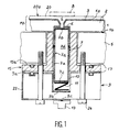
- FIG 1 there is shown, in section, an example of a connector of the invention with a part of the treatment reactor in which said connector finds one of its applications.
- the PS substrate holder, the connector, and a thermostatically controlled electrode 5 which is, during a plasma treatment, brought to a radio frequency voltage.
- the entire device is generally arranged (partially or totally) in a vacuum chamber, this chamber not being shown in the figure for the sake of simplification of said figure.
- the PS substrate holder also called a sample holder, comprises a flat conductive part 1, produced from a thick insulating sole 2 covered on its upper face with a thin conductive layer 3 acting as an opposite electrode. of the substrate 8 placed on said substrate holder.
- This substrate is isolated from the conductive layer by an insulating layer 20 disposed on the upper face 1a of the part 1.
- In the sole 2 are pierced openings (also called holes) 4 whose internal wall is also covered with a layer conductive 3.
- the vicinity of said holes 4, on the underside 1b of the substrate holder PS is covered with such a conductive layer 3.
- the sole / conductive layer assembly constitutes the flat conductive part of the substrate holder.
- holes 4 arranged opposite the connecting rods 7, and of a dimension substantially equal to 0.5 millimeter, for example, in their smallest diameter, are as numerous as the desired number of connections to the voltage source . Indeed, each hole 4 allows the establishment of a connector.
- the upper part of the holes 4 has a diameter greater than that of its lower part to allow better deposition of the conductive material 3 in said holes.
- the deposition of the conductive layer 3 on the insulating sole 2 and in the hole 4 is carried out, for example, by a thermal CVD process (in English: Chemical Vapor Deposition).
- a thermal CVD process in English: Chemical Vapor Deposition.
- the excess of conductive material deposited is eliminated so as not to put in direct contact the electrode 5 and said PS substrate holder. Only the conductive material deposited in the vicinity of the holes 4 is kept on this lower face 1b in order to ensure electrical contact with the connection rods 7.
- the substrate holder has on its face lower 1b, in the vicinity of the holes, a shoulder 6 increasing the electrical path between the electrode 5 and the layer of conductive material 6 which then partially covers the recess. This shoulder also provides support for the connection rod pushed by the spring 11 on the substrate holder.
- a flexible contact connector is used.
- This connector comprises the connection rod 7, movable in the connector, the base 9 and the elastic means 11 consisting, for example, of a conductive spring.
- connection rod 7 is a cylinder whose diameter is greater than the diameter of the hole 4.
- connection rod is electromagnetically shielded, that is to say that it has a high impedance.
- connection rod 7 it is made of an insulating material 7d (aluminum oxide, quartz, etc.) covered on its side walls 7a and its contact surfaces 7b and 7c with a film thin 7th of weakly conductive material (obtained, for example, by deposition of graphite or weakly doped silicon).
- the film thus obtained has, for example, a resistance of some 10 6 Ohms.
- connection rod 7 is made of a conductive material of high resistivity (having, for example, a resistance of some 10 6 Ohms), of the intrinsic silicon or carbon type.
- the rod 7 passes through the electrode 5 to connect the part 1 and the base 9. It comes into contact with the part 1 simply by applying the connector to the part 1.
- connection rod 7 may comprise, at its ends 7c and 7b, an additional layer 26a and 26b of metal (obtained, for example, from a silver lacquer, conductive paints, etc.) ensuring a better contact with the part 1 and the elastic means 11.
- connection rod 7 is made of an insulating material 7d covered with a thin film 7e of conductive material on its walls 7a and its upper contact surfaces 7b and lower 7c. Each of these contact surfaces 7b and 7c is covered in addition with a respective layer 26a and 26b of metal, so as to further increase the quality of the contact between the contact rod 7 and, respectively, the substrate holder 1 and the spring 11.
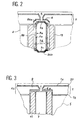
- FIG. 2 represents, in addition, the embodiment in which the upper contact surface 7b is chamfered, so as to improve the contact with the conductive layer 6 covering the shoulder of the opening 4.
- a more particular embodiment of this connecting rod consists in also chamfering the lower contact surface 7c of said contact rod and in covering it with a layer 26b of metal to improve its electrical contact with the spring 11.
- chamfers allow, on the one hand, easier adjustment between the contact rod and the shoulder of the substrate holder and, on the other hand, better electrical continuity of the conductive layers due to the elimination of sharp angles.
- the walls 7a of the connection rod 7, already covered with the thin film 7e are, moreover, covered with a layer 28 of passivation insulating material ensuring the 7th thin film protection.
- This layer 28 can be produced by depositing silica, by insulating paint, etc.
- the base 9 can also be produced according to several modes.
- the first embodiment of this base 9 is shown in FIG. 1.
- the base 9 is manufactured in the same insulating material as the connecting rod 7 and covered at least partially with the same thin conductive film 22, that is to say with a thin film of the same physical characteristics.
- the latter is made of a conductive material, such as copper, aluminum, etc.
- a resistance of high value for example a few 10 6 Ohms is connected between this voltage source and the base 9.
- This base 9 includes a recess 10 in which the lower part 7c of the connection rod 7 can be introduced. At the bottom of this recess 10, the conductive spring 11 is placed, which allows electrical continuity between the base 9 and the connection rod 7.
- This spring 11 also provides flexible contact between the substrate holder PS and the connector. Indeed, the spring 11 is positioned in the recess 10, and tends to constantly push the connection rod 7 upward so as to always apply the upper surface 7b (or contact surface) of the connection rod 7 on the conductive part of the lower face 1b of the substrate holder.
- connection 13 allows the connection of the connector to the power source, not shown in the figure.
- This connection 13 can be, for example, the base of an electrical outlet, for example of the standard BNC type, fixed to the contact surface 9C of the base.
- the base 9 is entirely covered with the thin conductive film 22.
- the bottom of the recess 10 in the base is also covered by a thin conductive layer so as to allow good contact with the spring 11.
- the spring being simply placed, it constitutes a soft connection.
- an additional deposit of conductive material of low resistance is made on the contact surfaces. resistive material.
- the contact surfaces 9b, 9c of said base, with, respectively, the spring 11 and the connection 13, are metallized.
- These metallizations ensure good electrical contact, that is to say a frank and reproducible electrical contact. Indeed, it is difficult to obtain frank electrical contact with a very resistive material such as that used in the invention, and more particularly when there is a soft bond between the two surfaces to be brought into contact.
- This metallization of the contact surfaces can be carried out for example by the thermal CVD process or by a curable coating, such as silver-charged epoxy resin applied locally to the surfaces to be metallized over the resistive material.
- an enclosure 15, made of a dielectric material makes it possible to isolate the connector brought to high voltage from the other elements of the reactor and, in particular, those coming from the radiofrequency electrodes 5.
- This enclosure 15 also surrounds, in its longitudinal part, the connection rod 7, that is to say that it surrounds the surfaces located outside the recess 10 and which do not have to establish electrical contact with the door - PS substrate.
- This enclosure 15 also covers the upper part 9a of the base 9 in order to ensure its electrical insulation with respect to the electrode.
- the enclosure 15 and the base 9 each have, on their respective upper surface 15a and 9a, an O-ring 17 making it possible to seal the connector vis-à-vis the reactor enclosure.
- the connector is moreover fixed to the electrode 5 by holding means, such as screws 24 which pass right through the base 9 and the enclosure 15.
- FIG 3 there is shown an embodiment of the support of the connection rod 7 on the substrate holder PS.
- a shoulder 6a of dimension greater than that of the shoulder 6 shown on figure 1
- the electric arcs capable of initiating parasitic currents are interrupted because they only very easily bypass an obstacle , namely the enclosure 15.
- This fitting of the enclosure 15 into the substrate holder takes place over a typical distance of 2 to 3 millimeters.
- connection not only can the connection be insensitive to electromagnetic radiation, but in addition, it is entirely removable, which allows simple maintenance. It is moreover made up of few parts, which allows an attractive manufacturing cost.
- the device described above in the description is applied to an electrostatic substrate holder. It is, of course, understood that it can be applied to all kinds of sample holders, or even to flat conductive parts used for purposes other than the processing of samples.
Landscapes
- Chemical & Material Sciences (AREA)
- Engineering & Computer Science (AREA)
- Physics & Mathematics (AREA)
- Chemical Kinetics & Catalysis (AREA)
- Mechanical Engineering (AREA)
- Computer Hardware Design (AREA)
- Microelectronics & Electronic Packaging (AREA)
- Power Engineering (AREA)
- General Physics & Mathematics (AREA)
- General Chemical & Material Sciences (AREA)
- Condensed Matter Physics & Semiconductors (AREA)
- Materials Engineering (AREA)
- Manufacturing & Machinery (AREA)
- Metallurgy (AREA)
- Organic Chemistry (AREA)
- Plasma & Fusion (AREA)
- Analytical Chemistry (AREA)
- Chemical Vapour Deposition (AREA)
- Multi-Conductor Connections (AREA)
- Container, Conveyance, Adherence, Positioning, Of Wafer (AREA)
Applications Claiming Priority (2)
| Application Number | Priority Date | Filing Date | Title |
|---|---|---|---|
| FR9113686A FR2683395A1 (fr) | 1991-11-06 | 1991-11-06 | Dispositif d'amende de tension sur une piece conductrice. |
| FR9113686 | 1991-11-06 |
Publications (2)
| Publication Number | Publication Date |
|---|---|
| EP0545748A1 EP0545748A1 (fr) | 1993-06-09 |
| EP0545748B1 true EP0545748B1 (fr) | 1997-01-29 |
Family
ID=9418669
Family Applications (1)
| Application Number | Title | Priority Date | Filing Date |
|---|---|---|---|
| EP19920402982 Expired - Lifetime EP0545748B1 (fr) | 1991-11-06 | 1992-11-04 | Dispositif d'amenée de tension sur un porte-substrat |
Country Status (3)
| Country | Link |
|---|---|
| EP (1) | EP0545748B1 (cg-RX-API-DMAC7.html) |
| DE (1) | DE69217187T2 (cg-RX-API-DMAC7.html) |
| FR (1) | FR2683395A1 (cg-RX-API-DMAC7.html) |
Cited By (1)
| Publication number | Priority date | Publication date | Assignee | Title |
|---|---|---|---|---|
| WO2022164529A1 (en) * | 2021-01-27 | 2022-08-04 | Applied Materials, Inc. | System for isolating electrodes at cryogenic temperatures |
Families Citing this family (2)
| Publication number | Priority date | Publication date | Assignee | Title |
|---|---|---|---|---|
| FR2724269B1 (fr) | 1994-09-06 | 1996-10-18 | Commissariat Energie Atomique | Porte-substrat electrostatique |
| US6221221B1 (en) | 1998-11-16 | 2001-04-24 | Applied Materials, Inc. | Apparatus for providing RF return current path control in a semiconductor wafer processing system |
Family Cites Families (4)
| Publication number | Priority date | Publication date | Assignee | Title |
|---|---|---|---|---|
| DE3012491C2 (de) * | 1980-03-31 | 1984-10-25 | Feinmetall Gmbh, 7033 Herrenberg | Kontaktbaustein zum Prüfen von elektrischen Leiterplatten |
| JPS59188550A (ja) * | 1983-04-12 | 1984-10-25 | Fuji Photo Film Co Ltd | イオン活量測定装置用電気接続端子アセンブリ− |
| EP0256541A3 (de) * | 1986-08-19 | 1990-03-14 | Feinmetall Gesellschaft mit beschrÀ¤nkter Haftung | Kontaktiervorrichtung |
| US4777908A (en) * | 1986-11-26 | 1988-10-18 | Optical Coating Laboratory, Inc. | System and method for vacuum deposition of thin films |
-
1991
- 1991-11-06 FR FR9113686A patent/FR2683395A1/fr active Granted
-
1992
- 1992-11-04 EP EP19920402982 patent/EP0545748B1/fr not_active Expired - Lifetime
- 1992-11-04 DE DE1992617187 patent/DE69217187T2/de not_active Expired - Fee Related
Cited By (1)
| Publication number | Priority date | Publication date | Assignee | Title |
|---|---|---|---|---|
| WO2022164529A1 (en) * | 2021-01-27 | 2022-08-04 | Applied Materials, Inc. | System for isolating electrodes at cryogenic temperatures |
Also Published As
| Publication number | Publication date |
|---|---|
| FR2683395B1 (cg-RX-API-DMAC7.html) | 1995-04-28 |
| DE69217187T2 (de) | 1997-07-17 |
| EP0545748A1 (fr) | 1993-06-09 |
| DE69217187D1 (de) | 1997-03-13 |
| FR2683395A1 (fr) | 1993-05-07 |
Similar Documents
| Publication | Publication Date | Title |
|---|---|---|
| EP0113273B1 (fr) | Boîtier d'encapsulation pour semiconducteur de puissance, à isolement entrée-sortie amélioré | |
| EP0792571A1 (fr) | Procede et dispositif de mesure d'un flux d'ions dans un plasma | |
| FR2700416A1 (fr) | Dispositif à semiconducteurs comportant un élément semiconducteur sur un élément de montage. | |
| FR2762748A1 (fr) | Dispositif d'excitation d'un gaz par plasma d'onde de surface | |
| EP0376387A1 (fr) | Dispositif incluant un porte-échantillons chauffant | |
| EP0263788B1 (fr) | Procédé et installation de dépôt de silicium amorphe hydrogène sur un substrat dans une enceinte à plasma | |
| FR2698234A1 (fr) | Structure de protection destinée à être utilisée dans un dispositif de circuit micro-ondes. | |
| EP3577683A1 (fr) | Structure pour application radiofréquence | |
| EP1586122A2 (fr) | Module photovoltaique comportant des bornes de connexion avec l exterieur | |
| EP0269485B1 (fr) | Dispositif de mesure formant un fluxmètre et un capteur de température combinés, constitué d'une structure multicouche, procédé de fabrication d'un tel dispositif et structure multicouche | |
| EP0545748B1 (fr) | Dispositif d'amenée de tension sur un porte-substrat | |
| FR2691035A1 (fr) | Dispositif et machine à plasma de traitement chimique et procédé utilisant ce dispositif. | |
| EP0228741B1 (fr) | Dispositif de test pour boîtier sans broches muni d'une pastille de circuit intégré hyperfréquences | |
| FR2725304A1 (fr) | Fusible pour microplaquette | |
| WO2014167193A1 (fr) | Machine d'implantation ionique presentant une productivite accrue | |
| EP0498700A1 (fr) | Procédé de fabrication d'un dispositif optoélectronique | |
| EP0044758A1 (fr) | Dispositif de terminaison d'une ligne de transmission, en hyperfréquence, à taux d'ondes stationnaires minimal | |
| FR2516311A1 (fr) | Socle pour le montage d'une pastille semi-conductrice sur l'embase d'un boitier d'encapsulation, et procede de realisation de ce socle | |
| EP0701319A1 (fr) | Porte-substrat électrostatique | |
| EP0232564B1 (fr) | Dispositif de test pour pastille de circuit intégré hyperfréquences | |
| FR2672398A1 (fr) | Dispositif electro-optique a guide d'onde. | |
| EP0586010A1 (fr) | Circuit pour des fréquences élevées, et procédé pour le réaliser | |
| WO2013093238A1 (fr) | Support comportant un porte-substrat électrostatique | |
| EP0480834B1 (fr) | Câble blindé formant élément de calibrage et procédé de réalisation d'un tel élément | |
| EP3430691B1 (fr) | Connecteur coaxial comprenant un shunt, assemblage et procédé de fabrication d'un tel connecteur |
Legal Events
| Date | Code | Title | Description |
|---|---|---|---|
| PUAI | Public reference made under article 153(3) epc to a published international application that has entered the european phase |
Free format text: ORIGINAL CODE: 0009012 |
|
| AK | Designated contracting states |
Kind code of ref document: A1 Designated state(s): BE CH DE FR GB LI NL |
|
| 17P | Request for examination filed |
Effective date: 19931118 |
|
| 17Q | First examination report despatched |
Effective date: 19950526 |
|
| GRAG | Despatch of communication of intention to grant |
Free format text: ORIGINAL CODE: EPIDOS AGRA |
|
| GRAH | Despatch of communication of intention to grant a patent |
Free format text: ORIGINAL CODE: EPIDOS IGRA |
|
| GRAH | Despatch of communication of intention to grant a patent |
Free format text: ORIGINAL CODE: EPIDOS IGRA |
|
| GRAA | (expected) grant |
Free format text: ORIGINAL CODE: 0009210 |
|
| AK | Designated contracting states |
Kind code of ref document: B1 Designated state(s): BE CH DE FR GB LI NL |
|
| REG | Reference to a national code |
Ref country code: CH Ref legal event code: EP |
|
| REF | Corresponds to: |
Ref document number: 69217187 Country of ref document: DE Date of ref document: 19970313 |
|
| GBT | Gb: translation of ep patent filed (gb section 77(6)(a)/1977) |
Effective date: 19970422 |
|
| PLBE | No opposition filed within time limit |
Free format text: ORIGINAL CODE: 0009261 |
|
| STAA | Information on the status of an ep patent application or granted ep patent |
Free format text: STATUS: NO OPPOSITION FILED WITHIN TIME LIMIT |
|
| 26N | No opposition filed | ||
| PGFP | Annual fee paid to national office [announced via postgrant information from national office to epo] |
Ref country code: BE Payment date: 19981103 Year of fee payment: 7 Ref country code: GB Payment date: 19981103 Year of fee payment: 7 |
|
| PGFP | Annual fee paid to national office [announced via postgrant information from national office to epo] |
Ref country code: DE Payment date: 19981116 Year of fee payment: 7 |
|
| PGFP | Annual fee paid to national office [announced via postgrant information from national office to epo] |
Ref country code: CH Payment date: 19981118 Year of fee payment: 7 |
|
| PGFP | Annual fee paid to national office [announced via postgrant information from national office to epo] |
Ref country code: FR Payment date: 19981127 Year of fee payment: 7 |
|
| PGFP | Annual fee paid to national office [announced via postgrant information from national office to epo] |
Ref country code: NL Payment date: 19981130 Year of fee payment: 7 |
|
| PG25 | Lapsed in a contracting state [announced via postgrant information from national office to epo] |
Ref country code: GB Free format text: LAPSE BECAUSE OF NON-PAYMENT OF DUE FEES Effective date: 19991104 |
|
| PG25 | Lapsed in a contracting state [announced via postgrant information from national office to epo] |
Ref country code: LI Free format text: LAPSE BECAUSE OF NON-PAYMENT OF DUE FEES Effective date: 19991130 Ref country code: CH Free format text: LAPSE BECAUSE OF NON-PAYMENT OF DUE FEES Effective date: 19991130 Ref country code: BE Free format text: LAPSE BECAUSE OF NON-PAYMENT OF DUE FEES Effective date: 19991130 |
|
| BERE | Be: lapsed |
Owner name: COMMISSARIAT A L'ENERGIE ATOMIQUE Effective date: 19991130 |
|
| PG25 | Lapsed in a contracting state [announced via postgrant information from national office to epo] |
Ref country code: NL Free format text: LAPSE BECAUSE OF NON-PAYMENT OF DUE FEES Effective date: 20000601 |
|
| GBPC | Gb: european patent ceased through non-payment of renewal fee |
Effective date: 19991104 |
|
| REG | Reference to a national code |
Ref country code: CH Ref legal event code: PL |
|
| PG25 | Lapsed in a contracting state [announced via postgrant information from national office to epo] |
Ref country code: FR Free format text: LAPSE BECAUSE OF NON-PAYMENT OF DUE FEES Effective date: 20000731 |
|
| NLV4 | Nl: lapsed or anulled due to non-payment of the annual fee |
Effective date: 20000601 |
|
| PG25 | Lapsed in a contracting state [announced via postgrant information from national office to epo] |
Ref country code: DE Free format text: LAPSE BECAUSE OF NON-PAYMENT OF DUE FEES Effective date: 20000901 |
|
| REG | Reference to a national code |
Ref country code: FR Ref legal event code: ST |