EP0544437B1 - Method for selectively growing aluminum-containing layers - Google Patents
Method for selectively growing aluminum-containing layers Download PDFInfo
- Publication number
- EP0544437B1 EP0544437B1 EP92310487A EP92310487A EP0544437B1 EP 0544437 B1 EP0544437 B1 EP 0544437B1 EP 92310487 A EP92310487 A EP 92310487A EP 92310487 A EP92310487 A EP 92310487A EP 0544437 B1 EP0544437 B1 EP 0544437B1
- Authority
- EP
- European Patent Office
- Prior art keywords
- gallium arsenide
- layer
- workpiece
- growth
- aluminum
- Prior art date
- Legal status (The legal status is an assumption and is not a legal conclusion. Google has not performed a legal analysis and makes no representation as to the accuracy of the status listed.)
- Expired - Lifetime
Links
Images

Classifications
-
- H—ELECTRICITY
- H10—SEMICONDUCTOR DEVICES; ELECTRIC SOLID-STATE DEVICES NOT OTHERWISE PROVIDED FOR
- H10D—INORGANIC ELECTRIC SEMICONDUCTOR DEVICES
- H10D10/00—Bipolar junction transistors [BJT]
- H10D10/01—Manufacture or treatment
- H10D10/021—Manufacture or treatment of heterojunction BJTs [HBT]
-
- H—ELECTRICITY
- H10—SEMICONDUCTOR DEVICES; ELECTRIC SOLID-STATE DEVICES NOT OTHERWISE PROVIDED FOR
- H10P—GENERIC PROCESSES OR APPARATUS FOR THE MANUFACTURE OR TREATMENT OF DEVICES COVERED BY CLASS H10
- H10P14/00—Formation of materials, e.g. in the shape of layers or pillars
- H10P14/20—Formation of materials, e.g. in the shape of layers or pillars of semiconductor materials
- H10P14/24—Formation of materials, e.g. in the shape of layers or pillars of semiconductor materials using chemical vapour deposition [CVD]
-
- H—ELECTRICITY
- H10—SEMICONDUCTOR DEVICES; ELECTRIC SOLID-STATE DEVICES NOT OTHERWISE PROVIDED FOR
- H10P—GENERIC PROCESSES OR APPARATUS FOR THE MANUFACTURE OR TREATMENT OF DEVICES COVERED BY CLASS H10
- H10P14/00—Formation of materials, e.g. in the shape of layers or pillars
- H10P14/20—Formation of materials, e.g. in the shape of layers or pillars of semiconductor materials
- H10P14/27—Formation of materials, e.g. in the shape of layers or pillars of semiconductor materials using selective deposition, e.g. simultaneous growth of monocrystalline and non-monocrystalline semiconductor materials
- H10P14/271—Formation of materials, e.g. in the shape of layers or pillars of semiconductor materials using selective deposition, e.g. simultaneous growth of monocrystalline and non-monocrystalline semiconductor materials characterised by the preparation of substrate for selective deposition
-
- H—ELECTRICITY
- H10—SEMICONDUCTOR DEVICES; ELECTRIC SOLID-STATE DEVICES NOT OTHERWISE PROVIDED FOR
- H10P—GENERIC PROCESSES OR APPARATUS FOR THE MANUFACTURE OR TREATMENT OF DEVICES COVERED BY CLASS H10
- H10P14/00—Formation of materials, e.g. in the shape of layers or pillars
- H10P14/20—Formation of materials, e.g. in the shape of layers or pillars of semiconductor materials
- H10P14/29—Formation of materials, e.g. in the shape of layers or pillars of semiconductor materials characterised by the substrates
- H10P14/2901—Materials
- H10P14/2907—Materials being Group IIIA-VA materials
- H10P14/2911—Arsenides
-
- H—ELECTRICITY
- H10—SEMICONDUCTOR DEVICES; ELECTRIC SOLID-STATE DEVICES NOT OTHERWISE PROVIDED FOR
- H10P—GENERIC PROCESSES OR APPARATUS FOR THE MANUFACTURE OR TREATMENT OF DEVICES COVERED BY CLASS H10
- H10P14/00—Formation of materials, e.g. in the shape of layers or pillars
- H10P14/20—Formation of materials, e.g. in the shape of layers or pillars of semiconductor materials
- H10P14/34—Deposited materials, e.g. layers
- H10P14/3402—Deposited materials, e.g. layers characterised by the chemical composition
- H10P14/3414—Deposited materials, e.g. layers characterised by the chemical composition being group IIIA-VIA materials
- H10P14/3418—Phosphides
-
- H—ELECTRICITY
- H10—SEMICONDUCTOR DEVICES; ELECTRIC SOLID-STATE DEVICES NOT OTHERWISE PROVIDED FOR
- H10P—GENERIC PROCESSES OR APPARATUS FOR THE MANUFACTURE OR TREATMENT OF DEVICES COVERED BY CLASS H10
- H10P14/00—Formation of materials, e.g. in the shape of layers or pillars
- H10P14/20—Formation of materials, e.g. in the shape of layers or pillars of semiconductor materials
- H10P14/34—Deposited materials, e.g. layers
- H10P14/3402—Deposited materials, e.g. layers characterised by the chemical composition
- H10P14/3414—Deposited materials, e.g. layers characterised by the chemical composition being group IIIA-VIA materials
- H10P14/3421—Arsenides
-
- H—ELECTRICITY
- H10—SEMICONDUCTOR DEVICES; ELECTRIC SOLID-STATE DEVICES NOT OTHERWISE PROVIDED FOR
- H10D—INORGANIC ELECTRIC SEMICONDUCTOR DEVICES
- H10D62/00—Semiconductor bodies, or regions thereof, of devices having potential barriers
- H10D62/80—Semiconductor bodies, or regions thereof, of devices having potential barriers characterised by the materials
- H10D62/85—Semiconductor bodies, or regions thereof, of devices having potential barriers characterised by the materials being Group III-V materials, e.g. GaAs
Definitions
- This invention relates to methods for fabricating gallium arsenide semiconductor devices and, in particular, to methods for selectively growing aluminum-containing layers such as aluminum gallium arsenide.
- gallium arsenide devices offer considerable promise for use as high speed electronic and photonic devices and integrated circuits.
- Such devices typically comprise a plurality of layers of gallium arsenide and aluminum gallium arsenide which are doped to n or p type conductivity and configured to operate as semiconductor electronic devices such as bipolar or field effect transistors or as photonic devices such as photodetectors or surface emitting lasers.
- a preferred method of fabricating a gallium arsenide layered structure is molecular beam epitaxy such as the process of metalorganic molecular beam epitaxy (MOMBE) described by G. J. Davies et al, 3 Chemtronics 3 (1988). Other molecular beam processes are described by W. T. Tsang, Journal of Electronic Materials , p. 235 (1986).
- MOMBE metalorganic molecular beam epitaxy
- a molecular beam process involves disposing a substrate within a low pressure growth chamber, heating the substrate and directing onto the substrate a molecular beam of gaseous molecules which decompose to form a desired layer.
- Processes referred to as MBE typically use only elemental sources for the Group III, Group V, and dopant elements, whereas MOMBE processes use a wide variety of elemental and compound gaseous sources providing at least one of the Group III or dopant elements.
- Typical MOMBE processes used in the fabrication of pnp and npn transistors are described in the related applications of C. R. Abernathy et al, and EP-A-0 501 686 and EP-A- 0 501 684.
- arsine AsH 3
- arsenic arsine or arsenic
- a number of device fabrication schemes require selective regrowth of aluminum gallium arsenide layers in unmasked limited areas of masked substrates. At desired low temperatures ( ⁇ 600°C) regrowth using arsine or arsenic is non-selective, leading to growth not only on the unmasked substrate but also upon the mask.
- PhAs phenylarsine
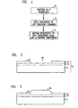
- FIG. 1 illustrates the steps in depositing an aluminum-containing layer
- FIGs. 2 and 3 show schematic cross sections of a typical workpiece before and after the deposition process of FIG. 1.
- the first step is to provide a workpiece 10 comprising a substrate 9 having a surface layer 13 of III-V semiconductor-of the gallium arsenide family.
- the workpiece 10 includes a masking layer 11 of silicon nitride exposing only a predetermined area 12 of a semiconductor layer 13.
- a workpiece can be the result of several preceding steps producing a desired stack of different doped semiconductor layers (not shown) in the region beneath mask 11 and even in the region underlying layer 13.
- the semiconductor can be any material in the gallium arsenide family including gallium arsenide, aluminum gallium arsenide, indium gallium arsenide, aluminum arsenide, aluminum indium arsenide, or aluminum indium phosphide.
- the next step shown in FIG. 1B is to heat the workpiece in an evacuated chamber which can be referred to as a growth chamber.
- the workpiece 10 is placed in a growth chamber, such as an INTEVAC Gas Source Gen II, evacuated to low pressure less than 0.013 Pa (10 -4 torr) and heated to a temperature in the range of 500°-550°C.
- a growth chamber such as an INTEVAC Gas Source Gen II
- the exposed semiconductor surface as formed is substantially free of impurities such as residual oxides or the surface is thoroughly cleaned in accordance with techniques well known in the art.
- the next step is exposing the semiconductor surface to gaseous molecules of phenylarsine and, at the same time, to a gaseous aluminium precursor such as trimethylamine alane (TMAAl).
- TMAAl trimethylamine alane
- the desired aluminum-containing material is AlGaAs
- the surface should also be exposed to a gaseous gallium precursor such as trimethylgallium (TMG).
- TMG trimethylgallium
- Phenylarsine is available from Air Products and Chemicals, Inc., Allentown, PA.
- the precursors are all introduced into the growth chamber via an H 2 carrier gas directed onto the substrate at a flow rate in the range 0.1 - 20 SCCM.
- H 2 carrier gas directed onto the substrate at a flow rate in the range 0.1 - 20 SCCM.
- the resulting structure is schematically illustrated in FIG. 3.
- the growth layer 14 is selectively formed on the semiconductor layer 13 and not on the mask layer 11.
- the mask layer 11 can be selectively removed, by dissolving silicon nitride in hot phosphoric acid.
- PhAs provides selective growth over a wider range of growth temperatures than arsine. In particular it provides selective growth at low temperatures (500°-550°C) desirable for the fabrication of semiconductor electronic and photonic devices.
- PhAs is particularly useful in selectively growing p-type layers of aluminum gallium arsenide because it does not preclude incorporation of carbon which for aluminum gallium arsenide, is a p-type dopant.
- FIG. 4 plots the concentration of various elements versus depth for successive layers grown using various precursors.
- TAG triethylgallium
- TMAAI trimethylamine alane
- arsine resulted in a carbon level of about 5x 10 16 cm -3 .
- the same group III fluxes were combined with phenylarsine, the carbon content was increased to about 1.8x10 18 cm -3 .
- FIG. 5 is a schematic view of a gallium arsenide device in the form of an "emitter-up" pnp transistor which can be advantageously fabricated using the inventive method.
- the device 40 depicted in FIG. 5 consists of a substrate 41 supporting successively grown layers 42, serving as transistor sub-collector, collector 43, and base region 44, in turn consisting of layers 45, 46, and 47. It is convenient to describe layer 46 as the functional base layer with embracing layers 45 and 47 (generally compositionally graded) serving as spacer regions (some in the art refer to the entirety of region 44 as the base region).
- the emitter layer 48 is followed by optional layer 49 and finally by layers 50 and 51, the three layers constituting the emitter contact region.
- DMAAs refers to tris-dimethylaminoarsenic, and the method of using DMAAs to form a gallium arsenide layer is described in applicant's copending application entitled “Method For Selectively Growing Gallium-Containing Layers” filed concurrently herewith (EP-A-0 544 438).
Description
- This invention relates to methods for fabricating gallium arsenide semiconductor devices and, in particular, to methods for selectively growing aluminum-containing layers such as aluminum gallium arsenide.
- Because of their high speeds and direct bandgap capabilities, gallium arsenide devices offer considerable promise for use as high speed electronic and photonic devices and integrated circuits. Such devices typically comprise a plurality of layers of gallium arsenide and aluminum gallium arsenide which are doped to n or p type conductivity and configured to operate as semiconductor electronic devices such as bipolar or field effect transistors or as photonic devices such as photodetectors or surface emitting lasers.
- A preferred method of fabricating a gallium arsenide layered structure is molecular beam epitaxy such as the process of metalorganic molecular beam epitaxy (MOMBE) described by G. J. Davies et al, 3 Chemtronics 3 (1988). Other molecular beam processes are described by W. T. Tsang, Journal of Electronic Materials, p. 235 (1986).
- In essence a molecular beam process involves disposing a substrate within a low pressure growth chamber, heating the substrate and directing onto the substrate a molecular beam of gaseous molecules which decompose to form a desired layer. Processes referred to as MBE typically use only elemental sources for the Group III, Group V, and dopant elements, whereas MOMBE processes use a wide variety of elemental and compound gaseous sources providing at least one of the Group III or dopant elements. Typical MOMBE processes used in the fabrication of pnp and npn transistors are described in the related applications of C. R. Abernathy et al, and EP-A-0 501 686 and EP-A- 0 501 684.
- One undesirable feature of prior art molecular beam processes is their use of arsine (AsH3) or arsenic as a source in the growth of aluminum gallium arsenide. A number of device fabrication schemes require selective regrowth of aluminum gallium arsenide layers in unmasked limited areas of masked substrates. At desired low temperatures (≤600°C) regrowth using arsine or arsenic is non-selective, leading to growth not only on the unmasked substrate but also upon the mask.
- Efforts to achieve selective AlGaAs growth have achieved only limited success. As or As2 adheres to the mask surface and catalyzes the decomposition of Al precursors. Growth temperatures in excess of 600°C are required to prevent nucleation of Al-containing materials on the mask surface. But for fabrication of many electronic devices, lower growth temperatures are desired. Accordingly, there is a need for improved methods for selectively growing aluminum-containing layers.
- Aluminium gallium arsenide layers are grown by molecular beam processes using as an arsenic precursor phenylarsine (PhAs). Because PhAs is more reactive than arsine and less reactive than arsenic, it decomposes selectively on III-V surfaces but not on mask materials. Thus in contrast to conventional processes, growth using PhAs permits selective growth on unmasked gallium arsenide surfaces but inhibits growth on typical mask materials such as silicon nitride.The growth takes place at a temperature in the range of 500° - 550°C.
- In the drawings:
- FIG. 1 is a block diagram showing the steps in growing an aluminum-containing layer;
- FIG. 2 is a schematic cross section of a typical workpiece upon which a layer of aluminum gallium arsenide can be grown;
- FIG. 3 shows the workpiece of FIG. 2 after growth;
- FIG. 4 is a graphical illustration of measured concentration versus depth using various precursors; and
- FIG. 5 is a schematic view of a preferred electronic device.
-
- Referring to the drawings, FIG. 1 illustrates the steps in depositing an aluminum-containing layer, and FIGs. 2 and 3 show schematic cross sections of a typical workpiece before and after the deposition process of FIG. 1.
- As shown in FIG. 1A the first step is to provide a
workpiece 10 comprising a substrate 9 having asurface layer 13 of III-V semiconductor-of the gallium arsenide family. - As shown in FIG. 2 the
workpiece 10 includes amasking layer 11 of silicon nitride exposing only apredetermined area 12 of asemiconductor layer 13. Such a workpiece can be the result of several preceding steps producing a desired stack of different doped semiconductor layers (not shown) in the region beneathmask 11 and even in theregion underlying layer 13. The semiconductor can be any material in the gallium arsenide family including gallium arsenide, aluminum gallium arsenide, indium gallium arsenide, aluminum arsenide, aluminum indium arsenide, or aluminum indium phosphide. - The next step shown in FIG. 1B is to heat the workpiece in an evacuated chamber which can be referred to as a growth chamber. The
workpiece 10 is placed in a growth chamber, such as an INTEVAC Gas Source Gen II, evacuated to low pressure less than 0.013 Pa (10-4 torr) and heated to a temperature in the range of 500°-550°C. Advantageously the exposed semiconductor surface as formed, is substantially free of impurities such as residual oxides or the surface is thoroughly cleaned in accordance with techniques well known in the art. - As shown in FIG. 1C, the next step is exposing the semiconductor surface to gaseous molecules of phenylarsine and, at the same time, to a gaseous aluminium precursor such as trimethylamine alane (TMAAl). Since, the desired aluminum-containing material is AlGaAs, the surface should also be exposed to a gaseous gallium precursor such as trimethylgallium (TMG). Phenylarsine is available from Air Products and Chemicals, Inc., Allentown, PA. Preferably the precursors are all introduced into the growth chamber via an H2 carrier gas directed onto the substrate at a flow rate in the range 0.1 - 20 SCCM. The result is selective epitaxial growth of aluminum gallium arsenide on the semiconductor surface at a rate on the order of 95 nm/min.
- The resulting structure is schematically illustrated in FIG. 3. As can be seen, the
growth layer 14 is selectively formed on thesemiconductor layer 13 and not on themask layer 11. If desired, themask layer 11 can be selectively removed, by dissolving silicon nitride in hot phosphoric acid. - This process using PhAs has many advantages over the prior use of arsine as an arsenic precursor. PhAs provides selective growth over a wider range of growth temperatures than arsine. In particular it provides selective growth at low temperatures (500°-550°C) desirable for the fabrication of semiconductor electronic and photonic devices.
- PhAs is particularly useful in selectively growing p-type layers of aluminum gallium arsenide because it does not preclude incorporation of carbon which for aluminum gallium arsenide, is a p-type dopant. The results of this effect can be seen by reference to FIG. 4 which plots the concentration of various elements versus depth for successive layers grown using various precursors. As illustrated growth with triethylgallium (TEG) trimethylamine alane (TMAAI) and arsine resulted in a carbon level of about 5x 1016cm-3. By contrast, when the same group III fluxes were combined with phenylarsine, the carbon content was increased to about 1.8x1018 cm-3.
- FIG. 5 is a schematic view of a gallium arsenide device in the form of an "emitter-up" pnp transistor which can be advantageously fabricated using the inventive method. The
device 40 depicted in FIG. 5 consists of asubstrate 41 supporting successively grownlayers 42, serving as transistor sub-collector,collector 43, andbase region 44, in turn consisting oflayers layer 46 as the functional base layer with embracinglayers 45 and 47 (generally compositionally graded) serving as spacer regions (some in the art refer to the entirety ofregion 44 as the base region). Next, theemitter layer 48 is followed byoptional layer 49 and finally bylayers - Table 1 below sets forth in detail the processes used to make this principal layers of the device of FIG. 5. The term DMAAs refers to tris-dimethylaminoarsenic, and the method of using DMAAs to form a gallium arsenide layer is described in applicant's copending application entitled "Method For Selectively Growing Gallium-Containing Layers" filed concurrently herewith (EP-A-0 544 438).
Growth Temperature = 525°C Layer
(Time:Thickness)Source Source Temp Carrier Gas Flow Rate Bubbler Pressure
(h Pa)50 Emitter TMG -9.4 5 80 Contact
(441 sec: 200nm)As H3 - 5 - 49 Graded Layer TMG -9.4 0.6 to 5 93 to 80 (140 sec:20nm) TMAA 9.2 7 to 0 9.3 PhAs 17 20 12. 3 48 Emitter TMGA -9.4 0.6 93 (800 sec:80nm) TMAA 9.2 7.0 9.3 PhAs 17 20 12. 3 47 Base TMGa -9.4 0.6 93 (220 sec:10nm) TMAAl 9.2 7.0 93 DMAAs 17 20 12. 3 46 Base TMGa -9.4 0.6 93 (26 sec:35nm) DMAAs 17 20 12. 3 45 Base TMGa -9.4 1.2 93 (300 sec:70nm) TESn -6.7 2.5 8 DMAAs 17 20 12. 3 44 Collector TMGa -9.4 4.0 93 (2000 sec:400nm) DMAAs 17 20 12. 3 AsH3. - 5.0 - 42 Sub-collector TMGa -9.4 5.0 80 (882 sec:400nm) AsH3 - 4.0 -
Claims (3)
- A method for growing a layer of aluminium gallium arsenide on a workpiece comprising the steps of:providing a workpiece including a surface layer of lll-V semiconductor material of the gallium arsenide family and further comprising a silicon nitride mask covering a portion of said surface layer while exposing selected portions;heating said workpiece in a reduced pressure chamber to a temperature in the range 500-550°C;exposing said workpiece to a gaseous aluminium precursor, a gaseous gallium precursor and PhAs so as to selectively grow a layer of aluminium gallium arsenide on said selected portions of said surface area.
- The method of claim 1, wherein said aluminium precursor comprises trimethylamine alane.
- The method of claim 1, wherein said gallium precursor comprises trimethylgallium.
Applications Claiming Priority (2)
| Application Number | Priority Date | Filing Date | Title |
|---|---|---|---|
| US79923891A | 1991-11-27 | 1991-11-27 | |
| US799238 | 1991-11-27 |
Publications (3)
| Publication Number | Publication Date |
|---|---|
| EP0544437A2 EP0544437A2 (en) | 1993-06-02 |
| EP0544437A3 EP0544437A3 (en) | 1993-09-01 |
| EP0544437B1 true EP0544437B1 (en) | 2003-09-17 |
Family
ID=25175389
Family Applications (1)
| Application Number | Title | Priority Date | Filing Date |
|---|---|---|---|
| EP92310487A Expired - Lifetime EP0544437B1 (en) | 1991-11-27 | 1992-11-18 | Method for selectively growing aluminum-containing layers |
Country Status (4)
| Country | Link |
|---|---|
| US (1) | US5459097A (en) |
| EP (1) | EP0544437B1 (en) |
| JP (1) | JP3392888B2 (en) |
| DE (1) | DE69233203T2 (en) |
Families Citing this family (2)
| Publication number | Priority date | Publication date | Assignee | Title |
|---|---|---|---|---|
| US6987055B2 (en) | 2004-01-09 | 2006-01-17 | Micron Technology, Inc. | Methods for deposition of semiconductor material |
| DE102009058786A1 (en) * | 2009-12-18 | 2011-06-22 | Fraunhofer-Gesellschaft zur Förderung der angewandten Forschung e.V., 80686 | Method for producing locally structured semiconductor layers |
Citations (3)
| Publication number | Priority date | Publication date | Assignee | Title |
|---|---|---|---|---|
| EP0501686A1 (en) * | 1991-02-28 | 1992-09-02 | AT&T Corp. | Fabrication of aluminium-containing semiconductor devices by metal-organic molecular-beam-epitaxy |
| EP0501684A2 (en) * | 1991-02-28 | 1992-09-02 | AT&T Corp. | Fabrication of GaAs devices with doped regions and devices so produced |
| EP0544438A2 (en) * | 1991-11-27 | 1993-06-02 | AT&T Corp. | Method for selectively growing gallium-containing layers |
Family Cites Families (2)
| Publication number | Priority date | Publication date | Assignee | Title |
|---|---|---|---|---|
| JPS5553415A (en) * | 1978-10-16 | 1980-04-18 | Mitsubishi Electric Corp | Selective epitaxial growing |
| JPH01308033A (en) * | 1988-06-07 | 1989-12-12 | Oki Electric Ind Co Ltd | Formation of oxide film |
-
1992
- 1992-11-18 DE DE69233203T patent/DE69233203T2/en not_active Expired - Lifetime
- 1992-11-18 EP EP92310487A patent/EP0544437B1/en not_active Expired - Lifetime
- 1992-11-27 JP JP31805092A patent/JP3392888B2/en not_active Expired - Lifetime
-
1993
- 1993-10-07 US US08/133,818 patent/US5459097A/en not_active Expired - Lifetime
Patent Citations (3)
| Publication number | Priority date | Publication date | Assignee | Title |
|---|---|---|---|---|
| EP0501686A1 (en) * | 1991-02-28 | 1992-09-02 | AT&T Corp. | Fabrication of aluminium-containing semiconductor devices by metal-organic molecular-beam-epitaxy |
| EP0501684A2 (en) * | 1991-02-28 | 1992-09-02 | AT&T Corp. | Fabrication of GaAs devices with doped regions and devices so produced |
| EP0544438A2 (en) * | 1991-11-27 | 1993-06-02 | AT&T Corp. | Method for selectively growing gallium-containing layers |
Non-Patent Citations (2)
| Title |
|---|
| AZOULAY R. ET AL.: "Selective MOCVD Epitaxy for Optoelectronic Devices", JOURNAL OF CRYSTAL GROWTH, vol. 55, pages 229 - 234 * |
| BRAUERS A. ET AL.: "The Use of Organic As Precursors in the Low Pressure MOCVD of GaAs", JOURNAL OF CRYSTAL GROWTH, vol. 93, no. 1-4, 1 November 1988 (1988-11-01), pages 7 - 14, XP000034986 * |
Also Published As
| Publication number | Publication date |
|---|---|
| EP0544437A2 (en) | 1993-06-02 |
| DE69233203D1 (en) | 2003-10-23 |
| JPH05226248A (en) | 1993-09-03 |
| DE69233203T2 (en) | 2004-05-06 |
| JP3392888B2 (en) | 2003-03-31 |
| EP0544437A3 (en) | 1993-09-01 |
| US5459097A (en) | 1995-10-17 |
Similar Documents
| Publication | Publication Date | Title |
|---|---|---|
| JP3760663B2 (en) | Method for producing group III nitride compound semiconductor device | |
| US5227006A (en) | Method for selectively growing gallium-containing layers | |
| EP0497350A1 (en) | Crystal growth method for gallium nitride-based compound semiconductor | |
| JP3189061B2 (en) | Method for manufacturing compound semiconductor device | |
| US5479028A (en) | III-V system compound semiconductor device and method for manufacturing the semiconductor device | |
| US5459097A (en) | Method for selectively growing aluminum-containing layers | |
| US6096617A (en) | Method of manufacturing a carbon-doped compound semiconductor layer | |
| JP3158651B2 (en) | Compound semiconductor and method of manufacturing the same | |
| JP3013992B2 (en) | Method for growing compound semiconductor crystal | |
| US5656540A (en) | Semiconductor crystal growing method | |
| JP3194327B2 (en) | Metalorganic vapor phase epitaxy | |
| JPH088460A (en) | Method of manufacturing p-type algan semiconductor | |
| JP2794506B2 (en) | Compound semiconductor heteroepitaxial growth method | |
| JP3134315B2 (en) | Method for selective growth of compound semiconductor crystal | |
| JP2651751B2 (en) | Compound semiconductor crystal growth method | |
| JP2853631B2 (en) | Method for producing gallium nitride single crystal thin film | |
| JPH0817739A (en) | Crystal growth method | |
| JP3213551B2 (en) | Method and apparatus for vapor phase growth of III-V compound semiconductors | |
| JP3421234B2 (en) | Semiconductor device and manufacturing method thereof | |
| JPH0766136A (en) | III-V Group Compound Semiconductor Epitaxial Growth Method | |
| JPH065514A (en) | Selective growth method for compound semiconductor thin film | |
| JPH08293639A (en) | Manufacture of semiconductor laser | |
| JPS6216517A (en) | Manufacture of compound semiconductor | |
| JPH05234907A (en) | Gaas substrate and its manufacture | |
| JPH07254564A (en) | Vapor phase epitaxial growth method |
Legal Events
| Date | Code | Title | Description |
|---|---|---|---|
| PUAI | Public reference made under article 153(3) epc to a published international application that has entered the european phase |
Free format text: ORIGINAL CODE: 0009012 |
|
| AK | Designated contracting states |
Kind code of ref document: A2 Designated state(s): DE GB |
|
| PUAL | Search report despatched |
Free format text: ORIGINAL CODE: 0009013 |
|
| AK | Designated contracting states |
Kind code of ref document: A3 Designated state(s): DE GB |
|
| 17P | Request for examination filed |
Effective date: 19940217 |
|
| RAP3 | Party data changed (applicant data changed or rights of an application transferred) |
Owner name: AT&T CORP. |
|
| 17Q | First examination report despatched |
Effective date: 19950802 |
|
| APAB | Appeal dossier modified |
Free format text: ORIGINAL CODE: EPIDOS NOAPE |
|
| APAD | Appeal reference recorded |
Free format text: ORIGINAL CODE: EPIDOS REFNE |
|
| APAD | Appeal reference recorded |
Free format text: ORIGINAL CODE: EPIDOS REFNE |
|
| APCB | Communication from the board of appeal sent |
Free format text: ORIGINAL CODE: EPIDOS OBAPE |
|
| APCB | Communication from the board of appeal sent |
Free format text: ORIGINAL CODE: EPIDOS OBAPE |
|
| APCB | Communication from the board of appeal sent |
Free format text: ORIGINAL CODE: EPIDOS OBAPE |
|
| GRAH | Despatch of communication of intention to grant a patent |
Free format text: ORIGINAL CODE: EPIDOS IGRA |
|
| GRAH | Despatch of communication of intention to grant a patent |
Free format text: ORIGINAL CODE: EPIDOS IGRA |
|
| GRAA | (expected) grant |
Free format text: ORIGINAL CODE: 0009210 |
|
| AK | Designated contracting states |
Kind code of ref document: B1 Designated state(s): DE GB |
|
| REG | Reference to a national code |
Ref country code: GB Ref legal event code: FG4D |
|
| REF | Corresponds to: |
Ref document number: 69233203 Country of ref document: DE Date of ref document: 20031023 Kind code of ref document: P |
|
| PLBE | No opposition filed within time limit |
Free format text: ORIGINAL CODE: 0009261 |
|
| 26N | No opposition filed |
Effective date: 20040618 |
|
| APAH | Appeal reference modified |
Free format text: ORIGINAL CODE: EPIDOSCREFNO |
|
| PGFP | Annual fee paid to national office [announced via postgrant information from national office to epo] |
Ref country code: DE Payment date: 20101119 Year of fee payment: 19 |
|
| PGFP | Annual fee paid to national office [announced via postgrant information from national office to epo] |
Ref country code: GB Payment date: 20101118 Year of fee payment: 19 |
|
| REG | Reference to a national code |
Ref country code: DE Ref legal event code: R071 Ref document number: 69233203 Country of ref document: DE |
|
| REG | Reference to a national code |
Ref country code: DE Ref legal event code: R071 Ref document number: 69233203 Country of ref document: DE |
|
| REG | Reference to a national code |
Ref country code: GB Ref legal event code: PE20 Expiry date: 20121117 |
|
| PG25 | Lapsed in a contracting state [announced via postgrant information from national office to epo] |
Ref country code: GB Free format text: LAPSE BECAUSE OF EXPIRATION OF PROTECTION Effective date: 20121117 |