EP0541304B1 - Monolithically integrated Fabry-Perot saturable absorber - Google Patents
Monolithically integrated Fabry-Perot saturable absorber Download PDFInfo
- Publication number
- EP0541304B1 EP0541304B1 EP92309954A EP92309954A EP0541304B1 EP 0541304 B1 EP0541304 B1 EP 0541304B1 EP 92309954 A EP92309954 A EP 92309954A EP 92309954 A EP92309954 A EP 92309954A EP 0541304 B1 EP0541304 B1 EP 0541304B1
- Authority
- EP
- European Patent Office
- Prior art keywords
- saturable absorber
- fabry
- layers
- optical
- perot
- Prior art date
- Legal status (The legal status is an assumption and is not a legal conclusion. Google has not performed a legal analysis and makes no representation as to the accuracy of the status listed.)
- Expired - Lifetime
Links
Images

Classifications
-
- H—ELECTRICITY
- H01—ELECTRIC ELEMENTS
- H01S—DEVICES USING THE PROCESS OF LIGHT AMPLIFICATION BY STIMULATED EMISSION OF RADIATION [LASER] TO AMPLIFY OR GENERATE LIGHT; DEVICES USING STIMULATED EMISSION OF ELECTROMAGNETIC RADIATION IN WAVE RANGES OTHER THAN OPTICAL
- H01S3/00—Lasers, i.e. devices using stimulated emission of electromagnetic radiation in the infrared, visible or ultraviolet wave range
- H01S3/10—Controlling the intensity, frequency, phase, polarisation or direction of the emitted radiation, e.g. switching, gating, modulating or demodulating
- H01S3/11—Mode locking; Q-switching; Other giant-pulse techniques, e.g. cavity dumping
- H01S3/1106—Mode locking
- H01S3/1109—Active mode locking
-
- G—PHYSICS
- G02—OPTICS
- G02F—OPTICAL DEVICES OR ARRANGEMENTS FOR THE CONTROL OF LIGHT BY MODIFICATION OF THE OPTICAL PROPERTIES OF THE MEDIA OF THE ELEMENTS INVOLVED THEREIN; NON-LINEAR OPTICS; FREQUENCY-CHANGING OF LIGHT; OPTICAL LOGIC ELEMENTS; OPTICAL ANALOGUE/DIGITAL CONVERTERS
- G02F1/00—Devices or arrangements for the control of the intensity, colour, phase, polarisation or direction of light arriving from an independent light source, e.g. switching, gating or modulating; Non-linear optics
- G02F1/01—Devices or arrangements for the control of the intensity, colour, phase, polarisation or direction of light arriving from an independent light source, e.g. switching, gating or modulating; Non-linear optics for the control of the intensity, phase, polarisation or colour
- G02F1/21—Devices or arrangements for the control of the intensity, colour, phase, polarisation or direction of light arriving from an independent light source, e.g. switching, gating or modulating; Non-linear optics for the control of the intensity, phase, polarisation or colour by interference
- G02F1/218—Devices or arrangements for the control of the intensity, colour, phase, polarisation or direction of light arriving from an independent light source, e.g. switching, gating or modulating; Non-linear optics for the control of the intensity, phase, polarisation or colour by interference using semi-conducting materials
-
- G—PHYSICS
- G02—OPTICS
- G02F—OPTICAL DEVICES OR ARRANGEMENTS FOR THE CONTROL OF LIGHT BY MODIFICATION OF THE OPTICAL PROPERTIES OF THE MEDIA OF THE ELEMENTS INVOLVED THEREIN; NON-LINEAR OPTICS; FREQUENCY-CHANGING OF LIGHT; OPTICAL LOGIC ELEMENTS; OPTICAL ANALOGUE/DIGITAL CONVERTERS
- G02F1/00—Devices or arrangements for the control of the intensity, colour, phase, polarisation or direction of light arriving from an independent light source, e.g. switching, gating or modulating; Non-linear optics
- G02F1/35—Non-linear optics
- G02F1/3523—Non-linear absorption changing by light, e.g. bleaching
-
- H—ELECTRICITY
- H01—ELECTRIC ELEMENTS
- H01S—DEVICES USING THE PROCESS OF LIGHT AMPLIFICATION BY STIMULATED EMISSION OF RADIATION [LASER] TO AMPLIFY OR GENERATE LIGHT; DEVICES USING STIMULATED EMISSION OF ELECTROMAGNETIC RADIATION IN WAVE RANGES OTHER THAN OPTICAL
- H01S3/00—Lasers, i.e. devices using stimulated emission of electromagnetic radiation in the infrared, visible or ultraviolet wave range
- H01S3/10—Controlling the intensity, frequency, phase, polarisation or direction of the emitted radiation, e.g. switching, gating, modulating or demodulating
- H01S3/11—Mode locking; Q-switching; Other giant-pulse techniques, e.g. cavity dumping
- H01S3/1106—Mode locking
- H01S3/1112—Passive mode locking
- H01S3/1115—Passive mode locking using intracavity saturable absorbers
- H01S3/1118—Semiconductor saturable absorbers, e.g. semiconductor saturable absorber mirrors [SESAMs]; Solid-state saturable absorbers, e.g. carbon nanotube [CNT] based
-
- G—PHYSICS
- G02—OPTICS
- G02F—OPTICAL DEVICES OR ARRANGEMENTS FOR THE CONTROL OF LIGHT BY MODIFICATION OF THE OPTICAL PROPERTIES OF THE MEDIA OF THE ELEMENTS INVOLVED THEREIN; NON-LINEAR OPTICS; FREQUENCY-CHANGING OF LIGHT; OPTICAL LOGIC ELEMENTS; OPTICAL ANALOGUE/DIGITAL CONVERTERS
- G02F2203/00—Function characteristic
- G02F2203/26—Pulse shaping; Apparatus or methods therefor
-
- H—ELECTRICITY
- H01—ELECTRIC ELEMENTS
- H01S—DEVICES USING THE PROCESS OF LIGHT AMPLIFICATION BY STIMULATED EMISSION OF RADIATION [LASER] TO AMPLIFY OR GENERATE LIGHT; DEVICES USING STIMULATED EMISSION OF ELECTROMAGNETIC RADIATION IN WAVE RANGES OTHER THAN OPTICAL
- H01S3/00—Lasers, i.e. devices using stimulated emission of electromagnetic radiation in the infrared, visible or ultraviolet wave range
- H01S3/05—Construction or shape of optical resonators; Accommodation of active medium therein; Shape of active medium
- H01S3/08—Construction or shape of optical resonators or components thereof
- H01S3/081—Construction or shape of optical resonators or components thereof comprising three or more reflectors
- H01S3/0813—Configuration of resonator
- H01S3/0817—Configuration of resonator having 5 reflectors, e.g. W-shaped resonators
Definitions
- This invention relates to saturable absorbing elements and, more particularly, to such elements utilized in combination with a Fabry-Perot etalon.
- Ultrashort optical pulses have durations in the picosecond and sub-picosecond range.
- Ultrashort optical pulses have been obtained by techniques such as passive modelocking wherein a nonlinear element is placed either within the lasing cavity or within a cavity external to the lasing cavity.
- a nonlinear element is a saturable absorber.
- Saturable absorbers are materials which display a change in opacity related to the incident radiation intensity at a particular wavelength. Solids, liquids, and gasses may be used as saturable absorbers based upon the chosen wavelength of operation.
- the saturable absorber acts as a shutter. It absorbs all weak radiation incident upon it. As the intensity of the incident radiation reaches a sufficiently high level called the saturation intensity of the saturable absorber, the incident radiation is permitted to pass through the absorber. In general, the attenuation of the incident radiation caused by the saturable absorber is relatively low because the absorber is saturated into a transparent state at the wavelength for the incident radiation.
- the nonlinearity and loss of a saturable absorber is determined effectively by the cross-section or thickness of the saturable absorber material traversed by the incident radiation. For thicker materials, a larger nonlinearity (saturation intensity) is achieved together with a larger loss for the saturable absorber; the thinner materials, a smaller nonlinearity is achieved together with a smaller amount of loss.
- the saturable absorber Whether used as an intra-cavity or external cavity element, the saturable absorber exhibits a nonlinearity and loss which are intimately coupled. This limits the design flexibility for known saturable absorbers because there is no available technique for designing the nonlinearity or saturation intensity independent from the loss of the saturable absorber.
- the preamble of claim 1 corresponds to US-A-4.071.831
- Degree of nonlinearity, that is, saturation intensity, and loss of a saturable absorber are substantially independently regulated by positioning a saturable absorber element within a Fabry-Perot etalon defined by first and second reflective elements so that the saturable absorber element responds to light at optical wavelengths in the anti-resonant portion of the Fabry-Perot spectral response, that is, between optical wavelengths corresponding to resonance peaks.
- the resulting combination of elements is called a Fabry-Perot saturable absorber.
- Thickness of the saturable absorber element substantially sets the loss of the Fabry-Perot saturable absorber while changes in the reflectivity of the first reflective element onto which the light is incident substantially determines the saturation intensity (degree of nonlinearity) and assists in compensating loss of the saturable absorber element.
- the Fabry-Perot saturable absorber has a free spectral range larger than the gain bandwidth of most lasers with which it would be used for modelocking, Q-switching and the like.
- a high reflectivity first reflective element is positioned on the end of the saturable absorber element facing the incident optical radiation while a similarly high reflectivity second reflective element is positioned on the opposite end of the saturable absorber.
- Dielectric material layers form the first reflective element whereas semiconductor layers form the second reflective element.
- a plurality of quantum well and barrier layers are employed to form the saturable absorber element.
- the second reflective element is formed by depositing a metallic film of the one end of the saturable absorber element.
- the Fabry-Perot saturable absorber is a monolithically integrated structure in which the saturable absorber element and the reflective elements are integrated in a single body.
- Such a monolithic structure is substantially insensitive to thermal loading, affords significant relaxation of design constraints, and substantially eliminates relative cavity length fluctuations, the latter giving rise to minimum duration optical pulses.
- the Fabry-Perot saturable absorber includes a high reflectivity element, it is contemplated that the Fabry-Perot saturable absorber be included as a cavity element coupled to a gain medium and a third reflective element on the opposite end of the gain medium from the Fabry-Perot saturable absorber. As such the Fabry-Perot saturable absorber is complete a laser structure which is capable of modelocked operation.
- Fabry-Perot saturable absorber 1 as shown in FIG. 1 includes reflective elements 2 and 3 and saturable absorber element 4. The reflective elements are separated in parallel to each other to form a Fabry-Perot etalon. Light is shown incident upon the Fabry-Perot saturable absorber at reflective element 2.
- Saturable absorber element 4 comprises a nonlinear material which is contemplated as being absorptive.
- Nonlinearity of the saturable absorber element is a function of the intensity of the incident optical radiation at or near a particular wavelength, the absorption cross-section, and the material thickness.
- the particular wavelength of operation is preferably in the anti-resonant band of the Fabry-Perot etalon.
- the anti-resonant band is understood to include the range of optical wavelengths between adjacent resonance wavelengths or resonant peak wavelengths for the Fabry-Perot etalon. By using this type of design, it is possible to achieve relaxation of thermal and other design constraints.
- the thickness or cross-section of saturable absorber element 4 is initially designed to set the loss at a desired value at the Fabry-Perot saturable absorber.
- Reflective elements 2 and 3 are contemplated as dielectric or semiconductor or metallic reflectors. Reflectivities for elements 2 and 3 are contemplated as varying over a wide range of values.
- reflective element 2 is the "input" for Fabry-Perot saturable absorber 1 which means that light (optical radiation) from a gain medium or a laser is incident initially upon reflective element 2.
- Fabry-Perot saturable absorber 1 which means that light (optical radiation) from a gain medium or a laser is incident initially upon reflective element 2.
- a gain medium such as a pumped Nd:YLF crystal or the like
- reflective element 2 together with another end reflective element as shown in FIG. 4 forms the laser cavity.
- reflective element 2 is required to have a reflectivity at or above 30%.
- the spacing of the reflective elements and the reflectivity of reflective element 2 are important.
- ⁇ the resonance wavelengths for the Fabry-Perot etalon
- the Fabry-Perot etalon has a maximum reflectivity and a round trip phase shift of an odd-integer multiple of ⁇ wherein the phase shift includes the penetration depth of both reflective elements 2 and 3.
- FIG. 2 An exemplary realization of the Fabry-Perot saturable absorber from FIG 1 is shown in cross-sectional view in FIG. 2.
- the Fabry-Perot saturable absorber in FIG. 2 comprises a semiconductor multiple quantum well structure as saturable absorber element 4 positioned between reflective elements 2 and 3.
- the semiconductor multiple quantum well structure is designed to have a bandgap in the quantum well substantially at or near the wavelength of the light incident on the Fabry-Perot saturable absorber. For the example shown in FIG.
- the bandgap of the quantum well layers is selected to correspond to 1.047 ⁇ m which is the light emission wavelength for a Nd:YLF crystal laser which may be used to radiate light incident on reflective element 2 of the Fabry-Perot saturable absorber.
- Saturable absorber element 4 shown in FIG 2 comprises an InGaAs/GaAs multiple quantum well structure.
- Barrier layers 41-1 through 41-N consist of 48 ⁇ thick GaAs while quantum well layers 42-1 through 42-N comprise 82 ⁇ thick In x Ga1 ⁇ x As, where the In concentration x is approximately 0.48 to achieve the quantum well energy bandgap close to the wavelength of incident light on the saturable absorber.
- There are fifty (N 50) periods of the quantum well/barrier pairs grown by epitaxial growth techniques over a semiconductor GaAs/AlAs reflector on a GaAs substrate. The number of periods employed together with the thickness of each layer determine the spacing between the reflective elements of the Fabry-Perot etalon.
- the spacing is set for the wavelength of incident light, that is, the wavelength for which the saturable absorber element 4 responds, to be in the anti-resonant band of the Fabry-Perot etalon.
- the spacing is approximately 0.65 ⁇ m.
- the wavelength of the incident light is near the center of the anti-resonant band substantially at the point of maximum reflectivity for the Fabry-Perot etalon between two adjacent resonance peaks of the Fabry-Perot etalon.
- Epitaxial growth of the quantum well structure is performed by low temperature molecular beam epitaxy (MBE) at approximately 380°C. This type of growth environment is utilized to reduce carrier lifetime and thereby achieve a relatively fast saturable absorber element 4. Carrier lifetime for the particular example described above is determined to be approximately 25 ps. Since low temperature growth increases the amount of unsaturable loss in the absorber element, it is understood that the Fabry-Perot saturable absorber as described herein exhibits less sensitivity to these unsaturable losses so that fast saturable absorber materials can be employed in the Fabry-Perot saturable absorber.
- the optical thickness of each layer is substantially equal to a quarter-wave thickness ( ⁇ /4n, where n is the effective refractive index for the particular layer) at the wavelength for the incident light.
- the thickness of GaAs layers 31-1 through 31-M is approximately 764 ⁇ while the thickness of AlAs layers 32-1 through 32-M is approximately 905 ⁇ .
- Standard MBE growth at 640 C is performed to realize reflective element 3 on GaAs substrate 50.
- the reflectivity of element 3 is high, approximately 96%, for the exemplary embodiment at the wavelength of the incident light. For the embodiment shown, a high reflectivity for element 3 is preferred to avoid thermal effects from damaging the structure.
- Reflective element 2 is shown in FIG. 2 as a stack of dielectric layers 21 and 22.
- Layers 21 and 22 are deposited TiO2 and SiO2, respectively, on the multiple quantum well structure of saturable absorber element 4. Reflectivity of element 2 in this example is approximately 98% at the wavelength of incident light. Techniques for depositing dielectric layers 21 and 22 and for determining the appropriate layer of thicknesses to achieve to desired reflectivity are well-known to persons skilled in the art and are not described herein. While element 2 is described in the example as comprising dielectric layers, it is understood that semiconductor layers having a similarly high reflectivity may be substituted therefor.
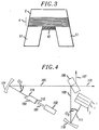
- FIG. 3 An alternative embodiment of the Fabry-Perot saturable absorber is shown in FIG. 3.
- elements 2 and 4 are understood to be as described above.
- Substrate 51 comprising GaAs is shown in the cross-sectional view as being etched to expose the end layer of saturable absorbable element 4. From FIG. 2, the exposed end layer is layer 42-N comprising InGaAs.
- metallic layer 43 comprising, for example, a thin deposited or evaporated layer of gold is employed as reflector element 3.
- Embodiments of the Fabry-Perot saturable absorber shown in FIGs. 2 and 3 have reflective elements monolithically integrated with the saturable absorber element. Monolithic integration of these elements prevents relative cavity length fluctuations and, therefore, optical wavelength fluctuations when the Fabry-Perot saturable absorber is used as a cavity element to mode lock a laser. Also, the monolithically integrated Fabry-Perot saturable absorber structure affords a minimum cavity length difference which, when the Fabry-Perot saturable absorber is used in conjunction with a laser gain medium, allows pulses of minimum duration to be realized.
- FIG. 4 shows an exemplary laser in which the Fabry-Perot saturable absorber is combined with a gain medium and reflector to provide continuous wave (cw) modelocking and Q-switching.
- the laser cavity shown in FIG. 4 is an end pumped, standing wave, folded cavity.
- Gain medium 103 is a 5 mm Nd:YLF crystal rod having the end surface normal to the main access of the rod coated for high reflection at the lasing wavelength thereby forming reflective element 113.
- Antireflection coating is also applied to this end of gain medium 103 wherein the antireflection coating has a characteristic wavelength corresponding to that of beam 101 from pump source 102.
- the opposite end of gain medium 103 is cut at the Brewster angle to form end surface 114.
- the lasing wavelength of gain medium 103 is approximately 1.047 ⁇ m and the wavelength of pump light 101 from pump source 102 is approximately 798 nm because pump source 102 comprises a cw Ti:Sapphire laser.
- Light from gain medium 103 is radiated from surface 114 to curved highly reflecting mirror 104 having a 200 mm radius of curvature.
- Mirror 104 is used to reduce for laser cavity mode diameter to an estimated spot size of 100 ⁇ m ⁇ 70 ⁇ m which is small enough to ensure a low pump power threshold.
- Beam 105 is directed off mirror 104 toward output coupler 106.
- Cavity output coupler 106 comprises a flat turning mirror having a 45 degree angle of incidence and 1% transmission to provide total output coupling of 2% via output beams 107 and 108. From cavity output coupler 106, beam 109 is focused onto the Fabry-Perot saturable absorber 112 by highly reflective curve mirror 110 having a radius of curvature of approximately 100 mm.
- the estimated spot radius of beam 111 as reflected by mirror 110 is approximately 40 ⁇ m.
- Fabry-Perot saturable absorber forms the other end mirror of the standing wave cavity, that is, the cavity defined by reflective elements 2 and 113. It should be noted that folding angles ⁇ 1 of approximately 16° and ⁇ 2 of approximately 12° substantially compensates astigmatism of the Brewster angle surface 114 of the Nd:YLF gain medium 103.
- Fabry-Perot saturable absorber 112 is the structure previously described in relation to FIG. 2.
- One important benefit of the Fabry-Perot saturable absorber design is that its free spectral range, which is approximately 100 nm for the structure in FIG. 2, is significantly larger than the gain bandwidth of the Nd:YLF laser which is approximately 0.6 nm.
- the Fabry-Perot saturable absorber relaxes many design constraints in the realization of a modelocked laser and eliminates sensitivities to thermal loading.
- the modelocked laser structure shown in FIG. 4 utilizing the Fabry-Perot saturable absorber is viewed as a coupled cavity structure where the main laser cavity is defined between reflective elements 2 and 113 and where the external nonlinear cavity including the saturable absorber is the Fabry-Perot saturable absorber 112. Both coupled cavities overlap interferometrically except for the saturable absorber element. This corresponds to a monolithic coupled cavity because any cavity length fluctuations in either cavity are identical in both cavities due to the presence of the Fabry-Perot saturable absorber. Cavity length detuning is minimized which, in turn, minimizes the duration of output optical pulses.
- the period of the coupled cavity structure is given as c/2 ⁇ L which corresponds to the free spectral range of a Fabry-Perot etalon having a thickness ⁇ L, where ⁇ L is the cavity length detuning between the two coupled cavities.
- Fabry-Perot saturable absorber 112 corresponds to the Fabry-Perot etalon having the desired thickness ⁇ L.
- the thickness of saturable absorber element 4 is judiciously set to realize a Fabry-Perot etalon whose free spectral range is larger than the gain bandwidth of the gain medium in order to prevent pulse width limitations by the Fabry-Perot etalon.
- the free spectral range of the etalon is larger than the gain bandwidth of the Nd:YLF gain medium.
- the outputs pulses had a sech pulse shape with a duration of 4ps at a repetition rate of approximately of 220MHz determined by the round-trip time of the cavity.
- This laser structure also exhibited a self-induced Q-switching characteristic with a pulse duration of 1.4 ⁇ seconds at a repetition rate of 120kHz, corresponding to the relaxation frequency of the Nd:YLF gain medium.
- Average output power for pulses from the laser in FIG. 4 was 480mW in response to 1.4W pump power from a cw Ti:sapphire laser at a wavelength of 798nm.
- the Fabry-Perot saturable absorber operates as a cavity saturable absorber at a particular wavelength for which it is possible to independently design the non-linearity, the loss, and the non-linearity speed (carrier lifetime) by choosing appropriate values for the reflectivity of reflective element 2, the thickness of saturable absorber element 4, and growth parameters relating to fabrication of the saturable absorber element.
- growth temperature in an epitaxial growth process can be used to achieve a desired response time for the saturable absorber element.
- the desired response time corresponds to the carrier lifetime.
- design of the non-linearity it is understood that for semiconductor materials the wavelength of operation determines the absorber cross-section and saturation intensity which determines the non-linearity.
- Fabry-Perot saturable absorber which are deemed obvious in view of the description above include the use of bulk semiconductor material for the saturable element.
- a broadband saturable absorber response is provided by compositionally grading the semiconductor saturable material or, in the case of semiconductor quantum wells, by varying the bandgap energy of successive wells from wide bandgap near reflective element 2 to narrow bandgap near reflective element 3.
- the thickness of quantum well layers andlor barrier layers can be varied to provide effective grading and therefore broadband operation.
- GaAs/InGaAs is described above for fabricating the saturable absorber element
- other material combinations may be selected from other semiconductor Group III-V systems such as GaAs/AlGaAs, InGaAs/InGaAlAs, InGaAs/InAlAs, GaAs/AlAs, GaAsSb/GaAlAsSb and InGaAsP/InP to achieve saturable absorption at different desired wavelengths.
- the layers may be lattice-matched to suitable GaAs or InP substrates. Mismatching is also contemplated wherein strained layers are grown over the substrate material.
- extension of the device structures is also contemplated to semiconductor compounds in Group II-VI and Group IV.
Landscapes
- Physics & Mathematics (AREA)
- Nonlinear Science (AREA)
- Optics & Photonics (AREA)
- Electromagnetism (AREA)
- Engineering & Computer Science (AREA)
- General Physics & Mathematics (AREA)
- Plasma & Fusion (AREA)
- Chemical & Material Sciences (AREA)
- Materials Engineering (AREA)
- Nanotechnology (AREA)
- Lasers (AREA)
Description
- This invention relates to saturable absorbing elements and, more particularly, to such elements utilized in combination with a Fabry-Perot etalon.
- Extremely short duration optical pulses are important for high speed signal processing and communications. Optical pulses in this category are commonly called ultrashort optical pulses and have durations in the picosecond and sub-picosecond range. Ultrashort optical pulses have been obtained by techniques such as passive modelocking wherein a nonlinear element is placed either within the lasing cavity or within a cavity external to the lasing cavity. One such nonlinear element is a saturable absorber.
- Saturable absorbers are materials which display a change in opacity related to the incident radiation intensity at a particular wavelength. Solids, liquids, and gasses may be used as saturable absorbers based upon the chosen wavelength of operation. The saturable absorber acts as a shutter. It absorbs all weak radiation incident upon it. As the intensity of the incident radiation reaches a sufficiently high level called the saturation intensity of the saturable absorber, the incident radiation is permitted to pass through the absorber. In general, the attenuation of the incident radiation caused by the saturable absorber is relatively low because the absorber is saturated into a transparent state at the wavelength for the incident radiation.
- In practice, the nonlinearity and loss of a saturable absorber is determined effectively by the cross-section or thickness of the saturable absorber material traversed by the incident radiation. For thicker materials, a larger nonlinearity (saturation intensity) is achieved together with a larger loss for the saturable absorber; the thinner materials, a smaller nonlinearity is achieved together with a smaller amount of loss. Whether used as an intra-cavity or external cavity element, the saturable absorber exhibits a nonlinearity and loss which are intimately coupled. This limits the design flexibility for known saturable absorbers because there is no available technique for designing the nonlinearity or saturation intensity independent from the loss of the saturable absorber. The preamble of
claim 1 corresponds to US-A-4.071.831 - Degree of nonlinearity, that is, saturation intensity, and loss of a saturable absorber are substantially independently regulated by positioning a saturable absorber element within a Fabry-Perot etalon defined by first and second reflective elements so that the saturable absorber element responds to light at optical wavelengths in the anti-resonant portion of the Fabry-Perot spectral response, that is, between optical wavelengths corresponding to resonance peaks. The resulting combination of elements is called a Fabry-Perot saturable absorber. Thickness of the saturable absorber element substantially sets the loss of the Fabry-Perot saturable absorber while changes in the reflectivity of the first reflective element onto which the light is incident substantially determines the saturation intensity (degree of nonlinearity) and assists in compensating loss of the saturable absorber element. The Fabry-Perot saturable absorber has a free spectral range larger than the gain bandwidth of most lasers with which it would be used for modelocking, Q-switching and the like.
- In one exemplary embodiment, a high reflectivity first reflective element is positioned on the end of the saturable absorber element facing the incident optical radiation while a similarly high reflectivity second reflective element is positioned on the opposite end of the saturable absorber. Dielectric material layers form the first reflective element whereas semiconductor layers form the second reflective element. A plurality of quantum well and barrier layers are employed to form the saturable absorber element.
- In another exemplary embodiment, the second reflective element is formed by depositing a metallic film of the one end of the saturable absorber element.
- For the latter exemplary embodiments, the Fabry-Perot saturable absorber is a monolithically integrated structure in which the saturable absorber element and the reflective elements are integrated in a single body. Such a monolithic structure is substantially insensitive to thermal loading, affords significant relaxation of design constraints, and substantially eliminates relative cavity length fluctuations, the latter giving rise to minimum duration optical pulses.
- Since the Fabry-Perot saturable absorber includes a high reflectivity element, it is contemplated that the Fabry-Perot saturable absorber be included as a cavity element coupled to a gain medium and a third reflective element on the opposite end of the gain medium from the Fabry-Perot saturable absorber. As such the Fabry-Perot saturable absorber is complete a laser structure which is capable of modelocked operation.
- A more complete understanding of the invention may be obtained by reading the following description of specific illustrative embodiments of the invention in conjunction with the appended drawing in which:
- FIG. 1 shows a simplified schematic of a Fabry-Perot saturable absorber;
- FIG. 2 depicts a cross-sectional view of a dielectric and semiconductor material layer structure for realizing the Fabry-Perot saturable absorber of FIG. 1;
- FIG. 3 is an alternative embodiment of the Fabry-Perot saturable absorber shown in FIG. 2; and
- FIG. 4 shows an application of the Fabry-Perot saturable absorber to laser modelocking.
- A Fabry-Perot saturable absorber is described below for performing passive saturable absorption useful for modelocking and Q-switching of lasers. Fabry-Perot saturable absorber 1 as shown in FIG. 1 includes
reflective elements reflective element 2. - Saturable absorber element 4 comprises a nonlinear material which is contemplated as being absorptive. Nonlinearity of the saturable absorber element is a function of the intensity of the incident optical radiation at or near a particular wavelength, the absorption cross-section, and the material thickness. For an absorptive nonlinearity utilized in accordance with the principles of this invention, the particular wavelength of operation is preferably in the anti-resonant band of the Fabry-Perot etalon. The anti-resonant band is understood to include the range of optical wavelengths between adjacent resonance wavelengths or resonant peak wavelengths for the Fabry-Perot etalon. By using this type of design, it is possible to achieve relaxation of thermal and other design constraints. The thickness or cross-section of saturable absorber element 4 is initially designed to set the loss at a desired value at the Fabry-Perot saturable absorber.
-
Reflective elements elements reflective element 2 is the "input" for Fabry-Perot saturable absorber 1 which means that light (optical radiation) from a gain medium or a laser is incident initially uponreflective element 2. When the light is from a gain medium such as a pumped Nd:YLF crystal or the like,reflective element 2 together with another end reflective element as shown in FIG. 4 forms the laser cavity. As suchreflective element 2 is required to have a reflectivity at or above 30%. In terms of the Fabry-Perot saturable absorber design, the spacing of the reflective elements and the reflectivity ofreflective element 2 are important. - Spacing L of
reflective elements 
reflective elements - An exemplary realization of the Fabry-Perot saturable absorber from FIG 1 is shown in cross-sectional view in FIG. 2. The Fabry-Perot saturable absorber in FIG. 2 comprises a semiconductor multiple quantum well structure as saturable absorber element 4 positioned between
reflective elements reflective element 2 of the Fabry-Perot saturable absorber. - Saturable absorber element 4 shown in FIG 2 comprises an InGaAs/GaAs multiple quantum well structure. Barrier layers 41-1 through 41-N consist of 48Å thick GaAs while quantum well layers 42-1 through 42-N comprise 82Å thick InxGa₁₋ xAs, where the In concentration x is approximately 0.48 to achieve the quantum well energy bandgap close to the wavelength of incident light on the saturable absorber. There are fifty (N=50) periods of the quantum well/barrier pairs grown by epitaxial growth techniques over a semiconductor GaAs/AlAs reflector on a GaAs substrate. The number of periods employed together with the thickness of each layer determine the spacing between the reflective elements of the Fabry-Perot etalon. In accordance with the principles of the invention, the spacing is set for the wavelength of incident light, that is, the wavelength for which the saturable absorber element 4 responds, to be in the anti-resonant band of the Fabry-Perot etalon. In the example, the spacing is approximately 0.65µm. For the layer thicknesses, number of periods, energy bandgap of the quantum well layers selected the wavelength of the incident light is near the center of the anti-resonant band substantially at the point of maximum reflectivity for the Fabry-Perot etalon between two adjacent resonance peaks of the Fabry-Perot etalon.
- No intentional doping is performed on this structure although doping of the semiconductor layers is contemplated for alternative embodiments. Epitaxial growth of the quantum well structure is performed by low temperature molecular beam epitaxy (MBE) at approximately 380°C. This type of growth environment is utilized to reduce carrier lifetime and thereby achieve a relatively fast saturable absorber element 4. Carrier lifetime for the particular example described above is determined to be approximately 25 ps. Since low temperature growth increases the amount of unsaturable loss in the absorber element, it is understood that the Fabry-Perot saturable absorber as described herein exhibits less sensitivity to these unsaturable losses so that fast saturable absorber materials can be employed in the Fabry-Perot saturable absorber. While low temperature MBE has been described above for realizing an exemplary saturable absorber element, other epitaxial growth techniques such as vapor phase epitaxy, liquid phase epitaxy and standard MBE are contemplated for realizing the Fabry-Perot saturable absorber and its constituent elements.
-
Reflective element 3 is shown in FIG. 2 as a stack of sixteen (M=16) periods of GaAs/AlAs layer pairs. The optical thickness of each layer is substantially equal to a quarter-wave thickness (λ/4n, where n is the effective refractive index for the particular layer) at the wavelength for the incident light. In the example, the thickness of GaAs layers 31-1 through 31-M is approximately 764Å while the thickness of AlAs layers 32-1 through 32-M is approximately 905Å. Standard MBE growth at 640 C is performed to realizereflective element 3 onGaAs substrate 50. The reflectivity ofelement 3 is high, approximately 96%, for the exemplary embodiment at the wavelength of the incident light. For the embodiment shown, a high reflectivity forelement 3 is preferred to avoid thermal effects from damaging the structure. -
Reflective element 2 is shown in FIG. 2 as a stack ofdielectric layers Layers element 2 in this example is approximately 98% at the wavelength of incident light. Techniques for depositingdielectric layers element 2 is described in the example as comprising dielectric layers, it is understood that semiconductor layers having a similarly high reflectivity may be substituted therefor. - An alternative embodiment of the Fabry-Perot saturable absorber is shown in FIG. 3. In this embodiment,
elements 2 and 4 are understood to be as described above.Substrate 51 comprising GaAs is shown in the cross-sectional view as being etched to expose the end layer of saturable absorbable element 4. From FIG. 2, the exposed end layer is layer 42-N comprising InGaAs. In order to complete the Fabry-Perot saturable absorber structure,metallic layer 43 comprising, for example, a thin deposited or evaporated layer of gold is employed asreflector element 3. - Embodiments of the Fabry-Perot saturable absorber shown in FIGs. 2 and 3 have reflective elements monolithically integrated with the saturable absorber element. Monolithic integration of these elements prevents relative cavity length fluctuations and, therefore, optical wavelength fluctuations when the Fabry-Perot saturable absorber is used as a cavity element to mode lock a laser. Also, the monolithically integrated Fabry-Perot saturable absorber structure affords a minimum cavity length difference which, when the Fabry-Perot saturable absorber is used in conjunction with a laser gain medium, allows pulses of minimum duration to be realized.
- FIG. 4 shows an exemplary laser in which the Fabry-Perot saturable absorber is combined with a gain medium and reflector to provide continuous wave (cw) modelocking and Q-switching. The laser cavity shown in FIG. 4 is an end pumped, standing wave, folded cavity.
Gain medium 103 is a 5 mm Nd:YLF crystal rod having the end surface normal to the main access of the rod coated for high reflection at the lasing wavelength thereby formingreflective element 113. Antireflection coating is also applied to this end ofgain medium 103 wherein the antireflection coating has a characteristic wavelength corresponding to that ofbeam 101 frompump source 102. The opposite end ofgain medium 103 is cut at the Brewster angle to formend surface 114. In this example, the lasing wavelength ofgain medium 103 is approximately 1.047µm and the wavelength of pump light 101 frompump source 102 is approximately 798 nm becausepump source 102 comprises a cw Ti:Sapphire laser. - Light from
gain medium 103 is radiated fromsurface 114 to curved highly reflectingmirror 104 having a 200 mm radius of curvature.Mirror 104 is used to reduce for laser cavity mode diameter to an estimated spot size of 100µm×70µm which is small enough to ensure a low pump power threshold.Beam 105 is directed offmirror 104 towardoutput coupler 106.Cavity output coupler 106 comprises a flat turning mirror having a 45 degree angle of incidence and 1% transmission to provide total output coupling of 2% viaoutput beams cavity output coupler 106,beam 109 is focused onto the Fabry-Perot saturable absorber 112 by highlyreflective curve mirror 110 having a radius of curvature of approximately 100 mm. The estimated spot radius ofbeam 111 as reflected bymirror 110 is approximately 40µm. Fabry-Perot saturable absorber forms the other end mirror of the standing wave cavity, that is, the cavity defined byreflective elements Brewster angle surface 114 of the Nd:YLF gain medium 103. - Fabry-Perot saturable absorber 112 is the structure previously described in relation to FIG. 2. One important benefit of the Fabry-Perot saturable absorber design is that its free spectral range, which is approximately 100 nm for the structure in FIG. 2, is significantly larger than the gain bandwidth of the Nd:YLF laser which is approximately 0.6 nm. In view of this design, the Fabry-Perot saturable absorber relaxes many design constraints in the realization of a modelocked laser and eliminates sensitivities to thermal loading.
- The modelocked laser structure shown in FIG. 4 utilizing the Fabry-Perot saturable absorber is viewed as a coupled cavity structure where the main laser cavity is defined between
reflective elements - When the Fabry-Perot saturable absorber is utilized in a coupled cavity mode locking laser structure, such as shown in FIG. 4, the thickness of saturable absorber element 4 is judiciously set to realize a Fabry-Perot etalon whose free spectral range is larger than the gain bandwidth of the gain medium in order to prevent pulse width limitations by the Fabry-Perot etalon. For the example shown in FIG. 4 and described above, the free spectral range of the etalon is larger than the gain bandwidth of the Nd:YLF gain medium.
- For the exemplary laser embodiment shown in FIG. 4, stable, self-starting, mode locked pulses were achieved. The outputs pulses had a sech pulse shape with a duration of 4ps at a repetition rate of approximately of 220MHz determined by the round-trip time of the cavity. This laser structure also exhibited a self-induced Q-switching characteristic with a pulse duration of 1.4µseconds at a repetition rate of 120kHz, corresponding to the relaxation frequency of the Nd:YLF gain medium. Average output power for pulses from the laser in FIG. 4 was 480mW in response to 1.4W pump power from a cw Ti:sapphire laser at a wavelength of 798nm.
- Advantageously, the Fabry-Perot saturable absorber operates as a cavity saturable absorber at a particular wavelength for which it is possible to independently design the non-linearity, the loss, and the non-linearity speed (carrier lifetime) by choosing appropriate values for the reflectivity of
reflective element 2, the thickness of saturable absorber element 4, and growth parameters relating to fabrication of the saturable absorber element. For example, growth temperature in an epitaxial growth process can be used to achieve a desired response time for the saturable absorber element. The desired response time corresponds to the carrier lifetime. With respect to design of the non-linearity, it is understood that for semiconductor materials the wavelength of operation determines the absorber cross-section and saturation intensity which determines the non-linearity. - Other contemplated embodiments of the Fabry-Perot saturable absorber which are deemed obvious in view of the description above include the use of bulk semiconductor material for the saturable element. Also, it is contemplated that a broadband saturable absorber response is provided by compositionally grading the semiconductor saturable material or, in the case of semiconductor quantum wells, by varying the bandgap energy of successive wells from wide bandgap near
reflective element 2 to narrow bandgap nearreflective element 3. Alternatively, the thickness of quantum well layers andlor barrier layers can be varied to provide effective grading and therefore broadband operation. These embodiments have not been shown in the FIGs. but are, after reading this specification, believed to be within the ordinary skill of persons in this field. - It is understood that, while the material system GaAs/InGaAs is described above for fabricating the saturable absorber element other material combinations may be selected from other semiconductor Group III-V systems such as GaAs/AlGaAs, InGaAs/InGaAlAs, InGaAs/InAlAs, GaAs/AlAs, GaAsSb/GaAlAsSb and InGaAsP/InP to achieve saturable absorption at different desired wavelengths. In these semiconductor systems, the layers may be lattice-matched to suitable GaAs or InP substrates. Mismatching is also contemplated wherein strained layers are grown over the substrate material. Finally, extension of the device structures is also contemplated to semiconductor compounds in Group II-VI and Group IV.
Claims (8)
- Optical apparatus comprising,first and second reflective elements (2;3,43) being spaced apart to form a Fabry-Perot etalon therebetween, said Fabry-Perot etalon having a plurality of optical resonance frequencies, andsemiconductor material (4) having a nonlinear optical absorption substantially at a predetermined optical frequency and being positioned between said first and second reflective elements (2;3,43), characterised by said predetermined optical frequency being between two adjacent optical resonance frequencies so that said predetermined optical frequency occurs substantially at an optical frequency corresponding to an anti-resonant condition for the Fabry-Perot etalon.
- The optical apparatus as defined in claim 1 wherein the first and second reflective elements (2;3,43) are monolithically integrated with said semiconductor material (4).
- The optical apparatus as defined in claim 2 wherein the semiconductor material (4) includes,first layers (41-1,41-N) of material having a first bandgap energy, andsecond layers (42-1,42-N) of material having a second bandgap energy, the first bandgap energy being larger than the second bandgap energy, the first layers alternated with the second layers to form a multiple quantum well structure, the thickness of the second layers being less than 500Å.
- The optical apparatus as defined in claim 3 wherein the first layers (41-1,41-N) comprise GaAs and the second layers (42-1,42-N) comprise a composition of InGaAs.
- The optical apparatus as defined in claim 2 wherein the semiconductor material (4) includes bulk semiconductor material.
- The optical apparatus as defined in claim 2 wherein the second reflective element (3) comprises,third layers (31-1,31-M) of semiconductor material having an optical thickness of one-quarter wavelength at the predetermined optical frequency, andfourth layers (32-1,32-M) of semiconductor material having an optical thickness of one-quarter wavelength at the predetermined optical frequency, said third and fourth layers being alternated with each other to form said second reflective element (3).
- The optical apparatus as defined in claim 6 wherein the third layers (31-1,31-M) include GaAs and the fourth layers (32-1,32-M) include AlAs.
- The optical apparatus as defined in claim 2 wherein the first reflective element (2) includes a fifth layer (21) comprising TiO₂ and a sixth layer (22) comprising SiO₂, the sixth layer (22) being adjacent to said semiconductor material (4) having the nonlinear optical absorption.
Applications Claiming Priority (2)
| Application Number | Priority Date | Filing Date | Title |
|---|---|---|---|
| US07/788,641 US5237577A (en) | 1991-11-06 | 1991-11-06 | Monolithically integrated fabry-perot saturable absorber |
| US788641 | 1991-11-06 |
Publications (2)
| Publication Number | Publication Date |
|---|---|
| EP0541304A1 EP0541304A1 (en) | 1993-05-12 |
| EP0541304B1 true EP0541304B1 (en) | 1996-01-24 |
Family
ID=25145114
Family Applications (1)
| Application Number | Title | Priority Date | Filing Date |
|---|---|---|---|
| EP92309954A Expired - Lifetime EP0541304B1 (en) | 1991-11-06 | 1992-10-30 | Monolithically integrated Fabry-Perot saturable absorber |
Country Status (4)
| Country | Link |
|---|---|
| US (1) | US5237577A (en) |
| EP (1) | EP0541304B1 (en) |
| JP (1) | JP2847006B2 (en) |
| DE (1) | DE69207862T2 (en) |
Cited By (1)
| Publication number | Priority date | Publication date | Assignee | Title |
|---|---|---|---|---|
| WO2019110345A1 (en) | 2017-12-06 | 2019-06-13 | Laser Zentrum Hannover E.V. | Optical element having alternating refractive index changes, and use thereof |
Families Citing this family (38)
| Publication number | Priority date | Publication date | Assignee | Title |
|---|---|---|---|---|
| ES2084358T3 (en) * | 1991-05-07 | 1996-05-01 | British Telecomm | OPTICAL REMOVAL OF THE CLOCK. |
| JP3424941B2 (en) * | 1992-04-01 | 2003-07-07 | 浜松ホトニクス株式会社 | Pulse light source device |
| US5303256A (en) * | 1993-03-12 | 1994-04-12 | Hughes Aircraft Company | Quasi-monolithic saturable optical element |
| US6301242B1 (en) | 1998-07-24 | 2001-10-09 | Xircom Wireless, Inc. | Communication system with fast control traffic |
| FR2715514B1 (en) * | 1994-01-21 | 1996-02-16 | Commissariat Energie Atomique | Laser with controllable beam direction. |
| US5436925A (en) * | 1994-03-01 | 1995-07-25 | Hewlett-Packard Company | Colliding pulse mode-locked fiber ring laser using a semiconductor saturable absorber |
| US5627854A (en) * | 1995-03-15 | 1997-05-06 | Lucent Technologies Inc. | Saturable bragg reflector |
| US6466604B1 (en) | 1995-05-19 | 2002-10-15 | Gigatera Ag | Optical component for generating pulsed laser radiation |
| US5666373A (en) * | 1996-02-06 | 1997-09-09 | Raytheon Company | Laser having a passive pulse modulator and method of making same |
| US5901162A (en) * | 1996-04-15 | 1999-05-04 | National Research Council Of Canada | Hybrid, saturable reflector for mode-locking lasers |
| US5701327A (en) * | 1996-04-30 | 1997-12-23 | Lucent Technologies Inc. | Saturable Bragg reflector structure and process for fabricating the same |
| US6141359A (en) * | 1998-01-30 | 2000-10-31 | Lucent Technologies, Inc. | Modelocking laser including self-tuning intensity-dependent reflector for self-starting and stable operation |
| JP3349945B2 (en) * | 1998-03-13 | 2002-11-25 | 日本電気株式会社 | Signal conversion device and optical transmission system using the signal conversion device |
| US5987049A (en) * | 1998-04-24 | 1999-11-16 | Time-Bandwidth Products Ag | Mode locked solid-state laser pumped by a non-diffraction-limited pumping source and method for generating pulsed laser radiation by pumping with a non-diffraction-limited pumping beam |
| EP1073933A1 (en) | 1998-04-30 | 2001-02-07 | Time-Bandwidth Products AG | Optically non-linear semiconductor material and a method for the production thereof |
| US6252892B1 (en) * | 1998-09-08 | 2001-06-26 | Imra America, Inc. | Resonant fabry-perot semiconductor saturable absorbers and two photon absorption power limiters |
| FR2784202B1 (en) * | 1998-10-05 | 2003-07-04 | Cit Alcatel | DEVICE FOR REGENERATING A WAVELENGTH MULTIPLEX SIGNAL COMPRISING A SATURABLE ABSORBENT |
| US6944201B2 (en) * | 1999-07-30 | 2005-09-13 | High Q Laser Production Gmbh | Compact ultra fast laser |
| US6400495B1 (en) | 2000-02-15 | 2002-06-04 | Massachusetts Institute Of Technology | Laser system including passively Q-switched laser and gain-switched laser |
| DE10009309B4 (en) * | 2000-02-26 | 2004-05-19 | Richter, Wolfgang, Dr. | Saturable semiconductor absorber |
| US6741619B1 (en) | 2000-04-03 | 2004-05-25 | Massachusetts Institute Of Technology | Semiconductor elements for stabilizing laser output |
| US6826205B1 (en) | 2000-05-22 | 2004-11-30 | Lightwave Electronics Corporation | Etalon enhanced saturable reflector for mode-locked lasers |
| JP2004505472A (en) | 2000-07-28 | 2004-02-19 | ダニエル コプフ | Lasers for use in nonlinear optics |
| US6658034B2 (en) * | 2000-12-13 | 2003-12-02 | Picarro, Inc. | Surface-emitting semiconductor laser |
| DE10109084A1 (en) * | 2001-02-24 | 2002-09-12 | Univ Karlsruhe | Optical element |
| FI113503B (en) * | 2002-03-13 | 2004-04-30 | Optoelectronics Res Ct | Procedure for organizing a mode-locked pulse queue by pump modulation |
| US6826219B2 (en) * | 2002-03-14 | 2004-11-30 | Gigatera Ag | Semiconductor saturable absorber device, and laser |
| DE10235712B4 (en) * | 2002-07-31 | 2008-04-24 | Jenoptik Laser, Optik, Systeme Gmbh | Method of operating a solid state laser and pulse laser with passive mode locking |
| WO2005020305A2 (en) * | 2003-08-12 | 2005-03-03 | Massachusetts Institute Of Technology | Optical device comprising crystalline semiconductor layer and reflective element |
| EP1517415A1 (en) * | 2003-09-18 | 2005-03-23 | Leica Geosystems AG | Geodetic apparatus with laser source |
| US7590156B1 (en) | 2004-05-17 | 2009-09-15 | University Of Central Florida Research Foundation, Inc. | High intensity MHz mode-locked laser |
| US20070045707A1 (en) * | 2005-08-31 | 2007-03-01 | Szu-Yu Wang | Memory device and manufacturing method thereof |
| WO2007071809A1 (en) * | 2005-12-22 | 2007-06-28 | Reflekron Oy | Semiconductor device and method to fabricate thereof |
| FR2904438B1 (en) * | 2006-07-26 | 2008-10-24 | Univ Paris Sud Etablissement P | PASSIVE COMPONENT OF ALL OPTICAL REGENERATION OF HIGH LEVELS BY CAVITY TO SATURABLE ABSORBENTS. |
| DE102008013925B3 (en) * | 2008-03-12 | 2009-05-07 | Batop Gmbh | Saturable absorber mirror for use as mode coupler for pulse lasers, has mechanical distance piece provided for changing thickness of air layer, which is formed between saturable absorber layer system and dielectric Bragg-mirror |
| FR3016743B1 (en) * | 2014-01-20 | 2016-03-04 | Centre Nat Rech Scient | PROCESS FOR PRODUCING SATURABLE ABSORBENT SEMICONDUCTOR MIRRORS |
| CN109412008A (en) * | 2018-10-26 | 2019-03-01 | 深圳大学 | Beta oxidation Asia lead quantum dot film and preparation method thereof, saturable absorber and Mode-locked laser device |
| JPWO2021171957A1 (en) * | 2020-02-27 | 2021-09-02 |
Family Cites Families (9)
| Publication number | Priority date | Publication date | Assignee | Title |
|---|---|---|---|---|
| US3610731A (en) * | 1969-05-19 | 1971-10-05 | Bell Telephone Labor Inc | Bistable optical circuit using saturable absorber within a resonant cavity |
| US4012699A (en) * | 1975-03-28 | 1977-03-15 | Bell Telephone Laboratories, Incorporated | Amplifying characteristics of a cavity-enclosed nonlinear medium |
| FR2333265A1 (en) * | 1975-11-28 | 1977-06-24 | Commissariat Energie Atomique | Shutter with optically controlled aperture - uses 2-mirror interferometer with body whose absorption may be saturated |
| US4597638A (en) * | 1983-02-28 | 1986-07-01 | At&T Bell Laboratories | Nonlinear optical apparatus |
| US4860296A (en) * | 1983-12-30 | 1989-08-22 | American Telephone And Telegraph Company, At&T Bell Laboratories | Laser controlled by a multiple-layer heterostructure |
| DE3474384D1 (en) * | 1983-12-30 | 1988-11-03 | American Telephone & Telegraph | Laser controlled by a multiple layer heterostructure |
| FR2589630B1 (en) * | 1985-07-23 | 1988-06-17 | Deveaud Benoit | SATURABLE ABSORBENT WITH VERY LOW SWITCHING TIMES |
| US4930131A (en) * | 1989-01-06 | 1990-05-29 | At&T Bell Laboratories | Source of high repetition rate, high power optical pulses |
| US5007059A (en) * | 1990-05-15 | 1991-04-09 | At&T Bell Laboratories | Nonlinear external cavity modelocked laser |
-
1991
- 1991-11-06 US US07/788,641 patent/US5237577A/en not_active Expired - Lifetime
-
1992
- 1992-10-30 DE DE69207862T patent/DE69207862T2/en not_active Expired - Lifetime
- 1992-10-30 EP EP92309954A patent/EP0541304B1/en not_active Expired - Lifetime
- 1992-11-06 JP JP4321448A patent/JP2847006B2/en not_active Expired - Lifetime
Cited By (1)
| Publication number | Priority date | Publication date | Assignee | Title |
|---|---|---|---|---|
| WO2019110345A1 (en) | 2017-12-06 | 2019-06-13 | Laser Zentrum Hannover E.V. | Optical element having alternating refractive index changes, and use thereof |
Also Published As
| Publication number | Publication date |
|---|---|
| US5237577A (en) | 1993-08-17 |
| EP0541304A1 (en) | 1993-05-12 |
| JP2847006B2 (en) | 1999-01-13 |
| JPH0667226A (en) | 1994-03-11 |
| DE69207862D1 (en) | 1996-03-07 |
| DE69207862T2 (en) | 1996-09-05 |
Similar Documents
| Publication | Publication Date | Title |
|---|---|---|
| EP0541304B1 (en) | Monolithically integrated Fabry-Perot saturable absorber | |
| EP0732613B1 (en) | Laser with a saturable Bragg reflector | |
| JP2724279B2 (en) | Laser system | |
| US5701327A (en) | Saturable Bragg reflector structure and process for fabricating the same | |
| US5345328A (en) | Tandem resonator reflectance modulator | |
| EP0609015B1 (en) | Antiresonant Fabry-Perot p-i-n modulator | |
| JP4559562B2 (en) | Resonant Fabry-Perot semiconductor saturable absorber and two-photon absorption power limiter | |
| MXPA97003090A (en) | Bragg saturable reflector structure and processed to manufacture the mi | |
| US20020135853A1 (en) | Photonic band gap device and method using a periodicity defect region doped with a gain medium to increase photonic signal delay | |
| EP0826164B1 (en) | Optical component for generating pulsed laser radiation | |
| EP1456916B1 (en) | Semiconductor saturable absorber mirror device | |
| US6141359A (en) | Modelocking laser including self-tuning intensity-dependent reflector for self-starting and stable operation | |
| US6826205B1 (en) | Etalon enhanced saturable reflector for mode-locked lasers | |
| JP2902996B2 (en) | Optical dispersion compensator, optical pulse generator and optical communication system using the same | |
| US6741619B1 (en) | Semiconductor elements for stabilizing laser output | |
| US5901162A (en) | Hybrid, saturable reflector for mode-locking lasers | |
| EP1071179B1 (en) | Saturable Bragg reflectors and their use in mode-locked lasers | |
| EP1130703A2 (en) | Hybrid semiconductor-dielectric chirped saturable absorber mirror | |
| EP1161783A1 (en) | Saturable bragg reflector with increased modulation depth | |
| McCall et al. | Operation of a GaAs-AIAs optical logic gate fabricated completely by molecular beam epitaxy | |
| Kubota et al. | Surface-emitting-laser-diode type wavelength selective filter | |
| Goldina et al. | Synthesis of dispersion-controlled mirror based on the semiconductor materials for near-IR femtosecond lasers | |
| JPH09244075A (en) | Light limitter element | |
| JP2002270929A (en) | Digital alloy modulation for manufacturing saturable absorber mirror | |
| WO2006120301A1 (en) | A mode-locked fiber laser |
Legal Events
| Date | Code | Title | Description |
|---|---|---|---|
| PUAI | Public reference made under article 153(3) epc to a published international application that has entered the european phase |
Free format text: ORIGINAL CODE: 0009012 |
|
| AK | Designated contracting states |
Kind code of ref document: A1 Designated state(s): DE FR GB |
|
| 17P | Request for examination filed |
Effective date: 19931028 |
|
| RAP3 | Party data changed (applicant data changed or rights of an application transferred) |
Owner name: AT&T CORP. |
|
| 17Q | First examination report despatched |
Effective date: 19950619 |
|
| GRAA | (expected) grant |
Free format text: ORIGINAL CODE: 0009210 |
|
| AK | Designated contracting states |
Kind code of ref document: B1 Designated state(s): DE FR GB |
|
| REF | Corresponds to: |
Ref document number: 69207862 Country of ref document: DE Date of ref document: 19960307 |
|
| ET | Fr: translation filed | ||
| PLBE | No opposition filed within time limit |
Free format text: ORIGINAL CODE: 0009261 |
|
| STAA | Information on the status of an ep patent application or granted ep patent |
Free format text: STATUS: NO OPPOSITION FILED WITHIN TIME LIMIT |
|
| 26N | No opposition filed | ||
| REG | Reference to a national code |
Ref country code: GB Ref legal event code: IF02 |
|
| PGFP | Annual fee paid to national office [announced via postgrant information from national office to epo] |
Ref country code: DE Payment date: 20101022 Year of fee payment: 19 |
|
| PGFP | Annual fee paid to national office [announced via postgrant information from national office to epo] |
Ref country code: GB Payment date: 20101021 Year of fee payment: 19 |
|
| PGFP | Annual fee paid to national office [announced via postgrant information from national office to epo] |
Ref country code: FR Payment date: 20111103 Year of fee payment: 20 |
|
| REG | Reference to a national code |
Ref country code: DE Ref legal event code: R071 Ref document number: 69207862 Country of ref document: DE |
|
| REG | Reference to a national code |
Ref country code: DE Ref legal event code: R071 Ref document number: 69207862 Country of ref document: DE |
|
| REG | Reference to a national code |
Ref country code: GB Ref legal event code: PE20 Expiry date: 20121029 |
|
| PG25 | Lapsed in a contracting state [announced via postgrant information from national office to epo] |
Ref country code: GB Free format text: LAPSE BECAUSE OF EXPIRATION OF PROTECTION Effective date: 20121029 |