EP0540799A1 - Improved AlGaInP diodes emitting visible light - Google Patents
Improved AlGaInP diodes emitting visible light Download PDFInfo
- Publication number
- EP0540799A1 EP0540799A1 EP91810848A EP91810848A EP0540799A1 EP 0540799 A1 EP0540799 A1 EP 0540799A1 EP 91810848 A EP91810848 A EP 91810848A EP 91810848 A EP91810848 A EP 91810848A EP 0540799 A1 EP0540799 A1 EP 0540799A1
- Authority
- EP
- European Patent Office
- Prior art keywords
- layer
- aigalnp
- doped
- layers
- cladding
- Prior art date
- Legal status (The legal status is an assumption and is not a legal conclusion. Google has not performed a legal analysis and makes no representation as to the accuracy of the status listed.)
- Withdrawn
Links
Images


Classifications
-
- H—ELECTRICITY
- H01—ELECTRIC ELEMENTS
- H01L—SEMICONDUCTOR DEVICES NOT COVERED BY CLASS H10
- H01L33/00—Semiconductor devices with at least one potential-jump barrier or surface barrier specially adapted for light emission; Processes or apparatus specially adapted for the manufacture or treatment thereof or of parts thereof; Details thereof
- H01L33/02—Semiconductor devices with at least one potential-jump barrier or surface barrier specially adapted for light emission; Processes or apparatus specially adapted for the manufacture or treatment thereof or of parts thereof; Details thereof characterised by the semiconductor bodies
- H01L33/04—Semiconductor devices with at least one potential-jump barrier or surface barrier specially adapted for light emission; Processes or apparatus specially adapted for the manufacture or treatment thereof or of parts thereof; Details thereof characterised by the semiconductor bodies with a quantum effect structure or superlattice, e.g. tunnel junction
- H01L33/06—Semiconductor devices with at least one potential-jump barrier or surface barrier specially adapted for light emission; Processes or apparatus specially adapted for the manufacture or treatment thereof or of parts thereof; Details thereof characterised by the semiconductor bodies with a quantum effect structure or superlattice, e.g. tunnel junction within the light emitting region, e.g. quantum confinement structure or tunnel barrier
-
- B—PERFORMING OPERATIONS; TRANSPORTING
- B82—NANOTECHNOLOGY
- B82Y—SPECIFIC USES OR APPLICATIONS OF NANOSTRUCTURES; MEASUREMENT OR ANALYSIS OF NANOSTRUCTURES; MANUFACTURE OR TREATMENT OF NANOSTRUCTURES
- B82Y20/00—Nanooptics, e.g. quantum optics or photonic crystals
-
- H—ELECTRICITY
- H01—ELECTRIC ELEMENTS
- H01S—DEVICES USING THE PROCESS OF LIGHT AMPLIFICATION BY STIMULATED EMISSION OF RADIATION [LASER] TO AMPLIFY OR GENERATE LIGHT; DEVICES USING STIMULATED EMISSION OF ELECTROMAGNETIC RADIATION IN WAVE RANGES OTHER THAN OPTICAL
- H01S5/00—Semiconductor lasers
- H01S5/20—Structure or shape of the semiconductor body to guide the optical wave ; Confining structures perpendicular to the optical axis, e.g. index or gain guiding, stripe geometry, broad area lasers, gain tailoring, transverse or lateral reflectors, special cladding structures, MQW barrier reflection layers
-
- H—ELECTRICITY
- H01—ELECTRIC ELEMENTS
- H01L—SEMICONDUCTOR DEVICES NOT COVERED BY CLASS H10
- H01L33/00—Semiconductor devices with at least one potential-jump barrier or surface barrier specially adapted for light emission; Processes or apparatus specially adapted for the manufacture or treatment thereof or of parts thereof; Details thereof
- H01L33/02—Semiconductor devices with at least one potential-jump barrier or surface barrier specially adapted for light emission; Processes or apparatus specially adapted for the manufacture or treatment thereof or of parts thereof; Details thereof characterised by the semiconductor bodies
- H01L33/26—Materials of the light emitting region
- H01L33/30—Materials of the light emitting region containing only elements of group III and group V of the periodic system
-
- H—ELECTRICITY
- H01—ELECTRIC ELEMENTS
- H01S—DEVICES USING THE PROCESS OF LIGHT AMPLIFICATION BY STIMULATED EMISSION OF RADIATION [LASER] TO AMPLIFY OR GENERATE LIGHT; DEVICES USING STIMULATED EMISSION OF ELECTROMAGNETIC RADIATION IN WAVE RANGES OTHER THAN OPTICAL
- H01S5/00—Semiconductor lasers
- H01S5/20—Structure or shape of the semiconductor body to guide the optical wave ; Confining structures perpendicular to the optical axis, e.g. index or gain guiding, stripe geometry, broad area lasers, gain tailoring, transverse or lateral reflectors, special cladding structures, MQW barrier reflection layers
- H01S5/2004—Confining in the direction perpendicular to the layer structure
- H01S5/2009—Confining in the direction perpendicular to the layer structure by using electron barrier layers
-
- H—ELECTRICITY
- H01—ELECTRIC ELEMENTS
- H01S—DEVICES USING THE PROCESS OF LIGHT AMPLIFICATION BY STIMULATED EMISSION OF RADIATION [LASER] TO AMPLIFY OR GENERATE LIGHT; DEVICES USING STIMULATED EMISSION OF ELECTROMAGNETIC RADIATION IN WAVE RANGES OTHER THAN OPTICAL
- H01S5/00—Semiconductor lasers
- H01S5/20—Structure or shape of the semiconductor body to guide the optical wave ; Confining structures perpendicular to the optical axis, e.g. index or gain guiding, stripe geometry, broad area lasers, gain tailoring, transverse or lateral reflectors, special cladding structures, MQW barrier reflection layers
- H01S5/22—Structure or shape of the semiconductor body to guide the optical wave ; Confining structures perpendicular to the optical axis, e.g. index or gain guiding, stripe geometry, broad area lasers, gain tailoring, transverse or lateral reflectors, special cladding structures, MQW barrier reflection layers having a ridge or stripe structure
-
- H—ELECTRICITY
- H01—ELECTRIC ELEMENTS
- H01S—DEVICES USING THE PROCESS OF LIGHT AMPLIFICATION BY STIMULATED EMISSION OF RADIATION [LASER] TO AMPLIFY OR GENERATE LIGHT; DEVICES USING STIMULATED EMISSION OF ELECTROMAGNETIC RADIATION IN WAVE RANGES OTHER THAN OPTICAL
- H01S5/00—Semiconductor lasers
- H01S5/30—Structure or shape of the active region; Materials used for the active region
- H01S5/32—Structure or shape of the active region; Materials used for the active region comprising PN junctions, e.g. hetero- or double- heterostructures
- H01S5/321—Structure or shape of the active region; Materials used for the active region comprising PN junctions, e.g. hetero- or double- heterostructures having intermediate bandgap layers
-
- H—ELECTRICITY
- H01—ELECTRIC ELEMENTS
- H01S—DEVICES USING THE PROCESS OF LIGHT AMPLIFICATION BY STIMULATED EMISSION OF RADIATION [LASER] TO AMPLIFY OR GENERATE LIGHT; DEVICES USING STIMULATED EMISSION OF ELECTROMAGNETIC RADIATION IN WAVE RANGES OTHER THAN OPTICAL
- H01S5/00—Semiconductor lasers
- H01S5/30—Structure or shape of the active region; Materials used for the active region
- H01S5/32—Structure or shape of the active region; Materials used for the active region comprising PN junctions, e.g. hetero- or double- heterostructures
- H01S5/323—Structure or shape of the active region; Materials used for the active region comprising PN junctions, e.g. hetero- or double- heterostructures in AIIIBV compounds, e.g. AlGaAs-laser, InP-based laser
- H01S5/32308—Structure or shape of the active region; Materials used for the active region comprising PN junctions, e.g. hetero- or double- heterostructures in AIIIBV compounds, e.g. AlGaAs-laser, InP-based laser emitting light at a wavelength less than 900 nm
- H01S5/32325—Structure or shape of the active region; Materials used for the active region comprising PN junctions, e.g. hetero- or double- heterostructures in AIIIBV compounds, e.g. AlGaAs-laser, InP-based laser emitting light at a wavelength less than 900 nm red laser based on InGaP
Definitions
- LEDs visible light emitting diodes
- the performance and reliability of these devices have to meet special requirements as there are e.g. high output power, continuous wave operation, low thermal and electrical resistance.
- Laser diodes consisting of AIGalInP/GalnP allow to fabricate lasers emitting lightwaves having wavelength lower than 700 nm.
- Different AIGalnP/GalnP device structures have been reported qualifying these types of lasers and LEDs to be the most promising ones for several future optoelectronic applications.
- AIGalnP/GalnP visible lasers and light emitting diodes are light sources which could be utilized for various optoelectronic applications including high-density optical disks, laser printers, plastic fiber com - munication, bar-code readers, pumping of solid state lasers, laser surgery and optical measurement systems which presently use He - Ne lasers.
- the following sections relate mainly to optical storage systems employing laser diodes.
- the require - ments of these laser diodes meet the requirements of laser diodes used in the other applications mentioned above.
- the semiconductor laser diode used for storing data on high-density optical disks is a key component because the wavelength of the radiation determines to a large extent the achievable storage density.
- Other requirements for these lasers are higher available optical power, which is limited by COD (Catastrophic Optical Damage) of the device, and improved reliability which is crucial for the overall system reliability.
- Known storage systems are based on AIGaAs lasers, lasing at a wavelength of 780 nm and reaching power levels of 30 mW. Laser diodes with reduced wavelength, improved optical output power and lifetime are important for future storage systems and the other optoelectronic applications mentioned.
- the quaternary AIGalnP lattice matched to GaAs, having a direct bandgap up to 2.3 eV, is presently the most interesting candidate for the above mentioned applications. Owing to advanced growth techniques, it has become possible to utilize the quaternary AIGalnP for diodes emitting in the range between 600 and 700 nm.
- One advantage of AIGalnP is the complete lattice match to crystalline quality binary GaAs substrate. In fact, almost all AIGalnP diodes reported today have been grown by MOVPE (Metal Organic Vapor Phase Epitaxy).
- DH visible light double - heterostructure
- the devices described in the above cited articles and patent applications have a simple double heterostructure.
- a comparable double heterostructure and its bandgap diagram are shown in Figure 1.
- the wavelength achieved by these lasers is typically between 670 and 690 nm. Their practical maximum output power up to now is, in lateral single mode narrow devices, less than 30 mW.
- the AIGalnP system per se is suitable for laser wavelength shorter than 670 nm.
- QW quantum well
- a typical MQW (Multi - Quantum Well) structure as disclosed in the above cited article of G.L Bona et al. and similar to the MQW structure described in the article of S. Kawata et al., is illustrated in Figure 2A.
- the corresponding bandgap diagram is shown in Figure 2B.
- the main improvement of this MQW device is its reduced threshold current (I thr ) and absorption losses (a) resulting in an improved efficiency ( ⁇ ).
- I thr threshold current
- a absorption losses
- ⁇ improved efficiency
- the maximum output power is furtheron limited by catastrophic optical damage (COD).
- This MQW structure consists of GalnP quantum wells sandwiched between undoped AIGalnP quantum barrier layers together being embedded between a p-doped AIGalnP cladding layer and a n-doped AIGalnP cladding layer.
- the wavelength of QW laser diodes in general is smaller than that of comparable DH laser diodes.
- AIGalnP/GalnP QW and MQW lasers emitting wavelength of 670 nm down to 625 nm have been reported in the literature.
- the maximum output power, limited by the COD of these devices, is reported to be about 10 - 30 mW, depending of the mode of operation, cooling, and geometry of the respective structure.
- the main object of this invention is to provide a semiconductor diode emitting visible light, which does not suffer or suffer at least to a considerably lesser extent from the limitations mentioned.
- Another object of the present invention is to provide a diode structure with improved performance.
- a further object is to provide a laser structure with reduced threshold current.
- the invention as claimed is intended to meet these objectives and to remedy the remaining deficiencies of known AIGalnP or AIGalnAs diodes.
- the principle by which this is accomplished is to provide for an active layer being embedded between thin AIGalnP (AIGalnAs) barrier layers and together sandwiched between thick AIGaAs (InP) cladding layers raising the COD level, reducing the electric resistance, and improving the differential quantum efficiency.
- the following description relates mainly to AIGalnP/GalnP quantum well and double - heterostructure loser diodes and LEDs, one embodiment disclosing the inventive structure being transferred into the long wavelength AIGalnAsP/lnP system.
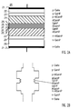
- a conventional DH loser diode 10 as for example disclosed in the article "Room-Temperature Pulsed Operation of AIGalnP/GalnP/AlGalnP Double Heterostructure Visible Light Laser Diodes Grown by Metalorganic Chemical Vapor Deposition", of I. Hino et al., Appl. Phys. Lett., Vol. 43 (11), December 1983, pp. 987 - 989, is illustrated in Figure 1A. Its bandgap diagram is shown in Figure 1B.
- the shown DH laser 10 consists of a GalnP active layer 14 being sandwiched between n- and p-doped AIGalnP cladding layers 15 and 13, the thickness of the active layer 15 being typically about 0,1 ⁇ m.
- the cladding layers 13 and 15 which consist of AIGalnP can be p-doped using Selenium (Se) and n-doped using Zinc (Zn).
- the cladding layers are about 1 ⁇ m thick.
- the structure is covered on one side by a p-doped GalnP bandgap matching layer 12 and a p-doped GaAs contact layer 11.
- the n-doped cladding layer 15 is situated on an n-doped bandgap matching layer 16, which consists of GaAs, and an n-doped GaAs substrate 17.
- Metal contacts 18.1 and 18.2 are situated at both sides of the device 10.
- Figure 2A shows a well known separate confinement MQW (Multi - Quantum Well) laser diode 20 being comparable with the DH diode 10 illustrated in Figure 1A.
- MQW Multi - Quantum Well
- the MQW structure 20, schematically shown in Figure 2A, consists of two undoped GalnP quantum wells 26.1, 26.2 embedded between, undoped or slightly doped AIGalnP waveguide layers 25.1 and 25.3.
- the quantum wells 26.1, 26.2 are separated by an undoped quantum barrier layer 25.1 and the whole quantum well structure is sandwiched between thick p - and n - doped cladding layers 24 and 27 consisting of AIGalnP.
- These cladding layers 24, 27 are followed by p- and n-doped GalnP bandgap matching layers 23 and 28.
- a p - doped contact layer 22 with metal contact 21.1 is situated on top of the device and an n-doped contact layer 29 with metal contact 21.2 on the opposite side.
- the bandgap diagram of the MQW layer sequence of Figure 2A is illustrated in Figure 2B.
- An example for the thickness of the layers can be given as follows: bandgap matching layers 23 and 28 about 0,1 ⁇ m, cladding layers 24 and 27 about 1 ⁇ m, waveguide layers 25.1 and 25.3 about 0,2 ⁇ m, quantum barrier layer 25.2 about 0,004 ⁇ m (4 nm), and quantum wells 0,2 ⁇ m.
- bandgap matching layers 23 and 28 about 0,1 ⁇ m
- cladding layers 24 and 27 about 1 ⁇ m
- waveguide layers 25.1 and 25.3 about 0,2 ⁇ m
- quantum barrier layer 25.2 about 0,004 ⁇ m (4 nm)
- quantum wells 0,2 ⁇ m.
- MQW lasers 23 - 24 has been shown that these MQW lasers exhibit significant lower threshold currents (I thr ) and higher efficiencies ( ⁇ ) in comparison to the DH diodes as for example shown in Figure 1A.
- MQW laser diodes emit shorter wavelength than comparable DH lasers.
- Some disadvantages of the devices known in the art are the high resistivity of the thick p - AIGalnP cladding layers caused by the low hole mobility of 10 - 20 cm 2 /Vs and large acceptor binding energy of > 100 meV. The power budget of these lasers is strongly determined by this. Growth of low resistive p-claddings requires incorporation of very high doping levels, running the risk that the pn -junction starts to displace uncontrollably due to diffusion of the dopants.
- the high thermal resistance of 17 Kcm/W of the AIGalnP layers forces to mount these lasers junction-down on a good heat sink. Even then, at a case temperature of 20 C, the junction temperature in cw (continuous wave) operation is typically already > 35 °C at threshold. In order to reduce this value, a thermally improved structure would be desirable.
- a key point of the invention is to replace a large fraction of the thick, former AIGalnP cladding layers against AIGaAs cladding layers 33 and 36.
- Very thin AIGalnP barrier layers 34.1, 34.2 are situated between these AIGaAs cladding layers 33, 36 and the active layer 35.
- the active recombination region i.e. the active layer 35
- the thickness of the former high Al - mole fraction AIGalnP cladding layers 34.1, 34.2 is reduced to a minimum, just avoiding tunneling and spill over of carriers from the active region into the AIGaAs cladding 33, 36.
- the thickness t b of the thin AIGalnP barrier layers 34.1, 34.2 can be much smaller than the wavelength ⁇ of the laser (t b « ⁇ ) such that these barrier layers 34.1 and 34.2 are not optically active.
- the quantum mechanical transmission probability T t hereinafter referred to as tunneling probability, can be described by the following equation: with where W is the thickness of the energy barrier, Eo is the height of this barrier, E is the energy of the carrier and m * their effective mass. When hW»1, the tunneling probability becomes
- the thickness of the barrier strongly effects the tunneling probability as can be seen from equation (3), which is mainly a problem of electrons (e-) because of their small m *.
- barrier thickness of at least 0,01 ⁇ m (10 nm) are required.
- the barrier thickness can be smaller according to the larger effective mass (m * ) of the holes. Good results can be achieved using quantum barrier layers with a thickness of about 0,0057 ⁇ m (5,7 nm) as reported in the article "Design and Photoluminescence Study on a Multiquantum Barrier", of T. Takagi et al., IEEE Journ. of Quantum Electronics, Vol. 27, No.
- Thin barrier layers can be grown lattice matched and strongly relaxed having a bandgap about 2,2 eV. Intentionally strained thin barrier layers could replace these relaxed layers thus allowing a modification of the barrier properties. e.g increasing their bandgap to be > 2,2 eV.
- the inventive laser diode 30, schematically shown in Figure 3A consists of a double heterostructure with GalnP active layer 35 embedded between a p-doped upper AIGalnP barrier layer 34.1 and an n-doped lower AIGalnP barrier layer 34.2.
- the thickness of these barrier layers 34.1 and 34.2 should preferably be between 0,01 and 0,1 ⁇ m.
- This layer sequence 34.1, 35, 34.2 is sandwiched between thick AIGaAs cladding layers 33, 36, the upper cladding layer 33 being p-doped and the lower cladding layer 36 being n-doped.
- Doped AIGaAs bandgap adaptation layers 32 and 37 are situated on these AIGaAs cladding layers 33 and 36 as bandgap adaptation to the outer contact layer 31 which consists of p-doped GaAs on one side and the n - doped GaAs substrate 38 on the other side.
- Broad metal contacts 39.1 and 39.2 are deposited on the top and bottom of the device 30.
- the AI - mole fraction at the contact and substrate side can be simply graded to zero, as for example shown in Figure 7B, which in addition helps to eliminate parasitic barriers.
- the AI (X AI ) fraction in the AIGaAs cladding layers has to be larger than 0,45 to prevent absorption of the laser light and to guide the wave efficiently.
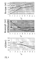
- the upper diagram of Figure 4 shows the bandgaps of AIGalnP and AIGaAs as functions of the AI fraction (X AI ), the middle diagram shows the wavelength in dependance of the AI fraction (X AI ), and the lower diagram shows the refractive indices of AIGalnP and AIGaAs as functions of the AI fraction (X AI ).
- Figure 3 shows a simple structure of a broad contact laser diode 30 with contact size 50 X 1000 ⁇ m 2 .
- This first embodiment can be simply modified by increasing or decreasing the thickness of the layers, inserting an unstrained MQW active structure or a strained MQW active structure replacing the active layer 35 described above.
- the inventive structure can be used in a ridge waveguide laser diode or a mesa stripe laser diode instead of the broad contact laser diode described above.
- Graded buffer layers can be employed as known in the art, replacing the bandgap adaptation layers.
- the second embodiment is a AIGalnP/GalnP separate confinement double heterostructure laser diode.
- a sketch of the corresponding bandgap diagram is shown in Figure 6.
- the undoped GalnP active layer of this embodiment is embedded between two undoped or slightly doped AIGalnP confinement layers. This active region is sandwiched between thin p - or n - doped AIGalnP barrier layers and thick p - or n - doped AIGaAs claddings, as illustrated in the bandgap diagram of Figure 6.
- FIG. 7 shows a schematic cross-section of a multi - quantum well structure and its bandgap diagram.
- This third embodiment is a MQW laser diode 70 its active region consisting of undoped GalnP active layers 76.1 and 76.2 (quantum wells) separated by a quantum barrier 75.2 and embedded between waveguide layers 75.1 and 75.3, these layers consisting of undoped or slightly p - and n-doped AIGalnP.
- This active region is embedded between an upper p-doped AIGalnP barrier layer 74.1 and a lower n-doped AIGalnP barrier layer 74.2.
- the outer layer sequences on both sides of the device is comparable to the sequence described before.
- the only difference is that the bandgap adaptation layers, layers 72 and 78 of the third embodiment, are graded bandgap layers as shown in Figure 7B.
- these graded bandgap layers 72, 78 it is possible to adapt the bandgap of the doped-AIGaAs claddings 73 and 77 to the contact layer 71 on one side and the substrate 79 on the other side.
- Exemplary details of the third embodiment are given in Table 2.
- This embodiment can be easily modified e.g. by replacing the shown active region 75.1 - 75.3, 76.1 and 76.2 against other multi-quantum well structures. Further modifications are illustrated in Figures 8 and 9. In both figures barrier layers with graded bandgaps are shown embedding the quantum well structure. A parabolic grading of optical confinment layers would be a further modification.
- FIG. 10 shows a cross-sectional view of an AIGalnP/GalnP laser diode 100 with ridge structure.
- the active region 107 shown as cross-hatched layer may consist of a double heterostructure or (multi -) quantum well structure as described before.
- This active region 107 is embedded between a thin upper p-doped AIGalnP barrier layer 106.1 and a thin lower n-doped AIGalnP barrier layer 106.2.
- the p-AlGaAs cladding 104 on top of the upper barrier layer 106.1 forms a ridge, exemplary shown having vertical sidewalls.
- a p-doped AIGaAs graded bandgap layer 103 and a p-doped GaAs contact layer are deposited on top of this cladding 104.
- the sidewalls of the ridge and the thin AIGalnP barrier are covered by a Si 3 N 4 insulating layer 105 and the whole structure is covered by a p - metal contact 101 which provides for an electrical contact to the contact layer 102.
- the whole layer sequence described above is situated on a substrate (not shown) carrying an n-doped AIGaAs cladding 108.
- the ridge structure is formed by etching, e.g dry-etching (RIE), the p-AIGaAs cladding layer 104.
- RIE dry-etching
- the thickness of the barrier layers 106.1 and 106.2 may be 0,05 ⁇ m and the thickness h of the ridge p-AIGaAs layer 104 about 2 ⁇ m.
- the ridge's width may be 5 ⁇ m and its length 500 ⁇ m. Exemplary details of the fourth embodiment are given in the following Table 3.
- a fifth embodiment is shown in Figure 11.
- a longer wavelength AIGalnAs/GalnAs/lnP laser diode 110 with ridge structure is illustrated.
- This structure is comparable to the one shown in Figure 10 but having thin AIGalnAs barrier layers 116.1 and 116.2 instead of AIGalnP barrier layers.
- the active layer 117 consists of (AI)GalnAs or GalnAsP and the cladding layers 114 and 118 consist of doped InP.
- This structure is grown on an InP substrate (not shown), the inclined surface of the ridge and the upper surface of the barrier layer 116.1 being covered by a Si 3 N 4 insulating layer 115.
- a graded bandgap layer 113, a GalnAs contact layer 112 and a Ti/Pt/Au contact 111 provides for the upper contact of the laser diode 110.
- the intensity-current curve of a conventional AIGalnP/GalnP laser diode, as described in context with Figure 2, and an intensity-current curve of a diode according to the invention are illustrated in Figure 12.
- the conventional AIGalnP/GalnP laser diode, its curve being marked with letter 'A', has a threshold current of about 50 mA and a COD level of typically 30 mW.
- the results of the inventive MQW laser diode (curve 'B') with 5 x 500 ⁇ m 2 ridge, described as one of the embodiments, has a threshold current of about 20,5 mA and a COD level about 340 mW. This COD level is about ten times as high as COD levels of known laser diodes. Both lasers were mounted junction side-up during the measurements and had uncoated mirrors.
Abstract
The invention concerns AIGalnP/GalnP visible laser diodes and LEDs with improved maximum output power. This is achieved by embedding the active region of the diode (30), e.g a GalnP active layer (35), between very thin p - and n - doped AIGalnP barrier layers (34.1, 34.2) and thick p - and n - doped AIGaAs cladding layers (33, 36). The inventive barrier layers (34.1, 34.2) are employed to avoid tunneling and spill over of carriers from the active region (35) into the cladding (33, 36). These barrier layers (34.1, 34.2) can be very thin thus allowing bandgap engineering and providing for barriers with low defect density. In addition the low resistance of the AIGaAs cladding reduces the thermal and electrical resistances of the device.
Description
- In some optoelectronic applications there is a special need for visible laser diodes lasing with a wavelength between 600 nm and 700 nm, and visible light emitting diodes (LEDs). The performance and reliability of these devices have to meet special requirements as there are e.g. high output power, continuous wave operation, low thermal and electrical resistance. Laser diodes consisting of AIGalInP/GalnP allow to fabricate lasers emitting lightwaves having wavelength lower than 700 nm. Different AIGalnP/GalnP device structures have been reported qualifying these types of lasers and LEDs to be the most promising ones for several future optoelectronic applications.
- AIGalnP/GalnP visible lasers and light emitting diodes are light sources which could be utilized for various optoelectronic applications including high-density optical disks, laser printers, plastic fiber com - munication, bar-code readers, pumping of solid state lasers, laser surgery and optical measurement systems which presently use He - Ne lasers.
- The following sections relate mainly to optical storage systems employing laser diodes. The require - ments of these laser diodes meet the requirements of laser diodes used in the other applications mentioned above. The semiconductor laser diode used for storing data on high-density optical disks is a key component because the wavelength of the radiation determines to a large extent the achievable storage density. Other requirements for these lasers are higher available optical power, which is limited by COD (Catastrophic Optical Damage) of the device, and improved reliability which is crucial for the overall system reliability. Known storage systems are based on AIGaAs lasers, lasing at a wavelength of 780 nm and reaching power levels of 30 mW. Laser diodes with reduced wavelength, improved optical output power and lifetime are important for future storage systems and the other optoelectronic applications mentioned.
- Different technical proposals are known to improve optical storage systems. One important development are devices emitting short wavelength which are based on second harmonic generation in non - linear optical material. The output power and reliability of these devices is not satisfying. The employment of improved AIGalnP/GalnP laser diodes with a wavelength of about 670 nm, increased output power and performance would allow for a 30 percent increase in storage density and an improved reliability of the whole storage system.
- The quaternary AIGalnP, lattice matched to GaAs, having a direct bandgap up to 2.3 eV, is presently the most interesting candidate for the above mentioned applications. Owing to advanced growth techniques, it has become possible to utilize the quaternary AIGalnP for diodes emitting in the range between 600 and 700 nm. One advantage of AIGalnP is the complete lattice match to crystalline quality binary GaAs substrate. In fact, almost all AIGalnP diodes reported today have been grown by MOVPE (Metal Organic Vapor Phase Epitaxy).
- Several AIGalnP visible light double - heterostructure (DH) lasers have been reported, most of them consisting of an undoped GalnP active layer embedded between a n-doped AIGalnP cladding layer and a p-doped AIGalnP cladding layer. A list of literature relating to these DH lasers is given below:
- - "Room-Temperature Pulsed Operation of AIGalnP/GalnP/AIGalnP Double Heterostructure Visible Light Laser Diodes Grown by Metalorganic Chemical Vapor Deposition", I. Hino et al., Appl. Phys. Lett., Vol. 43 (11), December 1983, pp. 987 - 989. In this article a double heterostructure laser diode is reported having an undoped GalnP active layer sandwitched between an n-doped lower AIGalnP cladding layer and a p-doped AIGalnP upper cladding layer, the double heterostructure being grown on top of a GaAs substrate.
- - "MOCVD Growth of (AlxGax-1)yln1-yP and Double Heterostructures for Visible Light Lasers", I. Hino, T. Suzuki, Journal of Crystal Growth, Vol. 68, 1984, pp. 483 - 489. I. Hino et al. report a DH structure in this article, consisting of the following stacked layers: GaAs substrate, n-AIGalnP cladding layer, undoped GalnP active layer, and p-AIGalnP cladding layer.
- - "Room - Temperature Continuous - Wave Operation of an AIGAInP Mesa Stripe Laser", M. Ikeda et al., Appl. Phys. Lett., Vol. 48 (2), January 1986, pp. 89 - 91. A DH structure consisting of an active GalnP layer embedded between p- and n-doped AIGalnP cladding layers and situated on top of a GaAs substrate is disclosed in this paper.
- - "Very Low Threshold Current Density of a GalnP/AIGalnP Double - Heterostructure Laser Grown by MOCVD", K. Nakano et al., Electronics Letters, Vol. 23, No. 17, August 1987, pp. 894 - 895. In this article, the authors report a conventional DH structure GalnP/AIGalnP laser diode grown on top of a GaAs substrate.
- - "Transverse - Mode - Stabilized Ridge Stripe AIGalnP Semiconductor Lasers Incorporating a Thin GaAs Etch-Stop Layer", T. Tanaka et al., Appl. Phys. Lett., Vol. 54 (15), April 1989, pp. 1391 - 1393. The laser diode described in this paper has a AIGalnP/GalnP heterostructure situated on top of a GaAs substrate.
- - "Semiconductor Laser Device and the Manufacturing Method thereof", European
Patent Application EP 0 328 393. This patent application discloses a DH laser diode consisting of AIGalnP/GalnP. - - "Manufacturing Method of Semiconductor Laser with non-absorbing Mirror Structure", European
Patent Application EP 0 373 933. Different DH laser diodes are reported in this application consisting of AIGalnP/GalnP. - - "Radiation-emitting Semiconductor Device and Method of Manufacturing such a Semiconductor", European
Patent Application EP 0 390 262. An AIGalnP/GalnP DH laser diode with ridge structure is disclosed in this application. - The devices described in the above cited articles and patent applications have a simple double heterostructure. A comparable double heterostructure and its bandgap diagram are shown in Figure 1. The wavelength achieved by these lasers is typically between 670 and 690 nm. Their practical maximum output power up to now is, in lateral single mode narrow devices, less than 30 mW. The AIGalnP system per se is suitable for laser wavelength shorter than 670 nm. Some laser diodes with wavelength of 680 nm and below have been reported as described in the following section.
- Analogous to the AIGaAs system, quantum well (QW) lasers can be realized with AIGalnP semicon - ductors. The wavelength of these devices is usually lower than that of comparable DH lasers. Exemplary literature relating to AIGalnP QW laser structures is listed below.
-
- - "Short - Wavelength (625 nm) Room-Temperature Continuous Laser Operation on ln0.5(AlxGa1-x)0.5P Quantum Well Heterostructures", D.W. Nam et al., Appl. Phys. Lett., Vol. 52 (16), April 1988, pp. 1329
- - 1331. D.W. Nam describes a AIGalnP/GalnP QW laser diode grown on a GaAs substrate.
- - "Room - Temperature, Continuous-Wave Operation for Mode-Stabilized AIGalnP Visible-Light Semiconductor Laser with a Multiquantum - Well Active Layer", S. Kawata et al., Electronics Letters, Vol. 24, No. 24, November 1988, pp. 1489 - 1490. A transverse mode stabilized AIGalnP/GalnP multi-quantum well laser diode is reported in this article.
- - "High Performance AIGalnP/GalnP MQW GRINSCH Lasers", P. Roentgen et al., 12th IEEE International Semiconductor Laser Conference, 9 September 1990, Davos, Post Deadline Papers, PD-11, pp. 23 - 24. P. Roentgen et al. present na AIGalnP/GalnP multi-quantum well graded index separate confinement heterostructure (GRINSCH) laser in this conference paper.
- - "High Quality Index Guided Ridge AIGalnP/GalnP Visible Lasers", G.L. Bona et al., 12th IEEE International Semiconductor Laser Conference, 9 September 1990, Davos, Conference Digest, L-3, pp. 178 - 179. Ridge lasers with AIGalnP/GalnP DH and MQW structure are disclosed in this paper.
- A typical MQW (Multi - Quantum Well) structure, as disclosed in the above cited article of G.L Bona et al. and similar to the MQW structure described in the article of S. Kawata et al., is illustrated in Figure 2A. The corresponding bandgap diagram is shown in Figure 2B. The main improvement of this MQW device is its reduced threshold current (Ithr) and absorption losses (a) resulting in an improved efficiency (η). However, the maximum output power is furtheron limited by catastrophic optical damage (COD). This MQW structure consists of GalnP quantum wells sandwiched between undoped AIGalnP quantum barrier layers together being embedded between a p-doped AIGalnP cladding layer and a n-doped AIGalnP cladding layer. The wavelength of QW laser diodes in general is smaller than that of comparable DH laser diodes. AIGalnP/GalnP QW and MQW lasers emitting wavelength of 670 nm down to 625 nm have been reported in the literature. The maximum output power, limited by the COD of these devices, is reported to be about 10 - 30 mW, depending of the mode of operation, cooling, and geometry of the respective structure.
- To come up with laser diodes lasing between 600 and 700 nm and having an improved maximum output power, additional improvements of these known structures are necessary. As known in the art the output power is limited by catastrophic optical damage (COD). The laser facets seem to play an important role in limiting the maximum output power. The temperature rise caused by lasing light absorption at the facets results into COD and destruction of the devices. Several proposals and structures are known improving the quality of the laser facets, most of them relating to AIGaAs lasers. Four articles disclosing methods and/or structures resulting in AIGalnP/GalnP lasers with increased output power are listed below.
-
- - "Novel Window-Structure AIGalnP Visible LDs with Non-Absorbing Facets Formed by Disordering of Natural Superlattice in GalnP Active Layer", Y. Ueno et al., 12th IEEE International Semiconductor Laser Conference, 9 September 1990, Davos, Conference Digest, C - 2, pp. 30 - 31;
- - "Novel Window - Structure AIGalnP Visible - Light Laser Diodes with Non-Absorbing Facets Fabricated by Utilizing GalnP Natural Superlattice Disordering", Y. Ueno et al., Jap. Journ. Appl. Phys., Vol. 29, No. 9, September 1990, pp. L 1666 - L 1668;
- - "Window-Structure InGaAIP Visible Light Laser Diodes by Self - Selective Diffusion Induced Disordering", K. Itaya et al., 12th IEEE International Semiconductor Laser Conference, 9 September 1990, Davos, Conference Digest, C - 5, pp. 36 - 37;
- - "Improvement of Catastrophic Optical Damage Level of AIGalnP Visible Laser Diodes by Sulfur Treatment", S. Kamiyama et al., Appl. Phys. Lett., Vol. 58 (23), June 1991, pp. 2595 - 2597; Recently, high - power visible laser diodes of up to 80 mW have been disclosed, having disordered active layers such that the light is hardly absorbed in a window region at the facets. The fabrication of these types of structures is complicated and expensive. As described in the article of S. Kamiyama et al., the COD level of AIGalnP laser diodes can be raised by a Sulfur treatment of the cleaved laser facets. COD levels of about 30 mW have been achieved as described in this article. Comparable windows structures with non - absorbing facets and treatments of the laser facets were known for AIGaAs laser diodes to be effective for increasing the maximum output power limited by COD.
- The main object of this invention is to provide a semiconductor diode emitting visible light, which does not suffer or suffer at least to a considerably lesser extent from the limitations mentioned.
- It is another object of this invention to provide a laser structure with improved COD level to increase the maximum output power.
- Another object of the present invention is to provide a diode structure with improved performance.
- A further object is to provide a laser structure with reduced threshold current.
- It is another object of this invention to provide a laser structure with high differential quantum efficiency.
- It is another object of this invention to provide a diode structure with low ohmic resistance.
- The invention as claimed is intended to meet these objectives and to remedy the remaining deficiencies of known AIGalnP or AIGalnAs diodes. The principle by which this is accomplished is to provide for an active layer being embedded between thin AIGalnP (AIGalnAs) barrier layers and together sandwiched between thick AIGaAs (InP) cladding layers raising the COD level, reducing the electric resistance, and improving the differential quantum efficiency.
- The invention is described in detail below with reference to the following drawings which are schematic and not drawn to scale, while more particularly the thickness of cross - sectional shown semiconductor layers are exaggerated for the sake of clarity.
-
- FIG.1A is a cross-section through a conventional double-heterostructure AIGalnP/GalnP laser diode.
- FIG. 1B is a bandgap diagram of the layer sequence of the double - heterostructure AIGalnP/GalnP laser shown in Figure 1A.
- FIG. 2A is a cross-section through a typical multi - quantum well AIGalnP/GalnP laser diode.
- FIG. 2B is a bandgap diagram of the layer sequence of the multi-quantum well AIGalnP/GalnP laser shown in Figure 2A.
- FIG. 3A is a cross-section through a double - heterostructure AIGalnP/GalnP laser diode with thin barrier layers and AIGaAs cladding, in accordance with the first embodiment of the present invention.
- FIG. 3B is a bandgap diagram of the layer sequence of the double - heterostructure AIGalnP/GalnP laser diode shown in Figure 3A.
- FIG 4 is a diagram showing the bandgaps, wavelength and refractive indexes of AIGalnP and AIGaAs as functions of the Aluminum fraction.
- FIG. 5 is a diagram showing the AlxGa1-xAS and (AlxGa1-x)yln1-yP composition dependance of the thermal resistance.
- FIG. 6 is a bandgap diagram of a simple separate confinement double - heterostructure layer sequence embedded between AIGalnP barrier layers and AIGaAs claddings, in accordance with the second embodiment of the present invention
- FIG. 7A is a cross-section through a multi-quantum well AIGalnP/GalnP laser diode with thin barrier layers and AIGaAs cladding, in accordance with the third embodiment of the present invention.
- FIG. 7B is a bandgap diagram of the layer sequence of the multi-quantum well AIGalnP/GalnP laser diode shown in Figure 7A.
- FIG. 8 is a bandgap diagram of a multi-quantum well AIGalnP/GalnP layer sequence embedded between thin AIGalnP barrier layers and AIGaAs claddings.
- FIG. 9 is a bandgap diagram of a multi-quantum well AIGalnP/GalnP layer sequence embedded between thin AIGalnP barrier layers and AIGaAs claddings.
- FIG. 10 is a cross-section through a AIGalnP/GalnP ridge laser diode with thin AIGalnP barrier layers and AIGaAs cladding, in accordance with the fourth embodiment of the present invention.
- FIG. 11 is a cross-section through a AIGalnAs/GalnAs ridge laser diode with thin AIGalnAs barrier layers and InP cladding, in accordance with the fifth embodiment of the present invention.
- FIG. 12 is an intensity versus current diagram of known MQW laser diode (A) as shown in Figure 2A and a MQW structure (B) with thin barrier layers and AIGaAs cladding, in accordance with the present invention.
- The following description relates mainly to AIGalnP/GalnP quantum well and double - heterostructure loser diodes and LEDs, one embodiment disclosing the inventive structure being transferred into the long wavelength AIGalnAsP/lnP system.
- A conventional
DH loser diode 10, as for example disclosed in the article "Room-Temperature Pulsed Operation of AIGalnP/GalnP/AlGalnP Double Heterostructure Visible Light Laser Diodes Grown by Metalorganic Chemical Vapor Deposition", of I. Hino et al., Appl. Phys. Lett., Vol. 43 (11), December 1983, pp. 987 - 989, is illustrated in Figure 1A. Its bandgap diagram is shown in Figure 1B. The shownDH laser 10 consists of a GalnPactive layer 14 being sandwiched between n- and p-doped AIGalnP cladding layers 15 and 13, the thickness of theactive layer 15 being typically about 0,1 µm. The cladding layers 13 and 15 which consist of AIGalnP can be p-doped using Selenium (Se) and n-doped using Zinc (Zn). The cladding layers are about 1 µm thick. The structure is covered on one side by a p-doped GalnPbandgap matching layer 12 and a p-dopedGaAs contact layer 11. The n-dopedcladding layer 15 is situated on an n-dopedbandgap matching layer 16, which consists of GaAs, and an n-dopedGaAs substrate 17. Metal contacts 18.1 and 18.2 are situated at both sides of thedevice 10. - Figure 2A shows a well known separate confinement MQW (Multi - Quantum Well)
laser diode 20 being comparable with theDH diode 10 illustrated in Figure 1A. For active region thickness equivalent to the de Broglie wavelength for thermalized electrons, the hole and electron energy levels become quantized in a manner given by the bound state energies of a finite square potential well. This effect is used in the quantum well laser diodes. - The
MQW structure 20, schematically shown in Figure 2A, consists of two undoped GalnP quantum wells 26.1, 26.2 embedded between, undoped or slightly doped AIGalnP waveguide layers 25.1 and 25.3. The quantum wells 26.1, 26.2 are separated by an undoped quantum barrier layer 25.1 and the whole quantum well structure is sandwiched between thick p - and n - doped cladding layers 24 and 27 consisting of AIGalnP. These cladding layers 24, 27 are followed by p- and n-doped GalnP bandgap matching layers 23 and 28. A p - doped contact layer 22 with metal contact 21.1 is situated on top of the device and an n-dopedcontact layer 29 with metal contact 21.2 on the opposite side. The bandgap diagram of the MQW layer sequence of Figure 2A is illustrated in Figure 2B. An example for the thickness of the layers can be given as follows: bandgap matching layers 23 and 28 about 0,1 µm, cladding layers 24 and 27 about 1 µm, waveguide layers 25.1 and 25.3 about 0,2 µm, quantum barrier layer 25.2 about 0,004 µm (4 nm), andquantum wells - Some disadvantages of the devices known in the art are the high resistivity of the thick p - AIGalnP cladding layers caused by the low hole mobility of 10 - 20 cm2/Vs and large acceptor binding energy of > 100 meV. The power budget of these lasers is strongly determined by this. Growth of low resistive p-claddings requires incorporation of very high doping levels, running the risk that the pn -junction starts to displace uncontrollably due to diffusion of the dopants.
- When growing thick AIGalnP cladding layers by MOVPE on a slightly misoriented GaAs substrate, the formation of large defects is a serious problem. The number and extension of this defects strongly increase with higher Al - content and larger layer thickness. This effect can be somewhat reduced by using stronger misoriented substrates or using extremely high PH3 flows during growth. Although there is no definitive proof, we have clear indications that the defects influence the laser performance, e.g. yield, and reliability of visible AIGalnP lasers.
- Additionally to the high ohmic resistance, the high thermal resistance of 17 Kcm/W of the AIGalnP layers forces to mount these lasers junction-down on a good heat sink. Even then, at a case temperature of 20 C, the junction temperature in cw (continuous wave) operation is typically already > 35 °C at threshold. In order to reduce this value, a thermally improved structure would be desirable.
- A key point of the invention, as described in connection with the first embodiment illustrated in Figure 3A, is to replace a large fraction of the thick, former AIGalnP cladding layers against AIGaAs cladding layers 33 and 36. Very thin AIGalnP barrier layers 34.1, 34.2 are situated between these AIGaAs cladding layers 33, 36 and the active layer 35. As seen in Figures 3A and 3B, the active recombination region, i.e. the active layer 35, remains unchanged, whereas the thickness of the former high Al - mole fraction AIGalnP cladding layers 34.1, 34.2 is reduced to a minimum, just avoiding tunneling and spill over of carriers from the active region into the AIGaAs cladding 33, 36. The thickness tb of the thin AIGalnP barrier layers 34.1, 34.2 can be much smaller than the wavelength λ of the laser (tb«λ) such that these barrier layers 34.1 and 34.2 are not optically active. The quantum mechanical transmission probability Tt, hereinafter referred to as tunneling probability, can be described by the following equation:

with
where W is the thickness of the energy barrier, Eo is the height of this barrier, E is the energy of the carrier and m* their effective mass. When hW»1, the tunneling probability becomes
- The thickness of the barrier strongly effects the tunneling probability as can be seen from equation (3), which is mainly a problem of electrons (e-) because of their small m*. To prevent tunneling of e through the barrier layers 34.1 and 34.2, barrier thickness of at least 0,01 µm (10 nm) are required. To prevent holes (h) from tunneling through a barrier, the barrier thickness can be smaller according to the larger effective mass (m*) of the holes. Good results can be achieved using quantum barrier layers with a thickness of about 0,0057 µm (5,7 nm) as reported in the article "Design and Photoluminescence Study on a Multiquantum Barrier", of T. Takagi et al., IEEE Journ. of Quantum Electronics, Vol. 27, No. 6, June 1991, pp. 1511 - 1517. Thin barrier layers can be grown lattice matched and strongly relaxed having a bandgap about 2,2 eV. Intentionally strained thin barrier layers could replace these relaxed layers thus allowing a modification of the barrier properties. e.g increasing their bandgap to be > 2,2 eV.
- By the employment of disordered barrier layers instead of ordered layers a further possibility is given to modify the properties of the barriers. As disclosed in the article "Evidence for the Existence of an Ordered State in Gao.51no.5P grown by Metalorganic Vapor Phase Epitaxy and its Relation to Band-gap Energy", of A. Gomyo et al., Appl. Phys. Lett., 50 (11), March 1987, pp. 673 - 675, the bandgap energy of metalorganic vapor phase epitaxially (MOVPE) grown Ga0.5ln0.5P is a function of a wide range of V/III ratios and growth temperatures. By growing the barrier layers such that the Ga-In-distribution on the column III element sublattice is different from the ordered, regularly arranged, Ga-In-distribution, the bandgap can be modified.
- The
inventive laser diode 30, schematically shown in Figure 3A, consists of a double heterostructure with GalnP active layer 35 embedded between a p-doped upper AIGalnP barrier layer 34.1 and an n-doped lower AIGalnP barrier layer 34.2. The thickness of these barrier layers 34.1 and 34.2 should preferably be between 0,01 and 0,1 µm. This layer sequence 34.1, 35, 34.2 is sandwiched between thick AIGaAs cladding layers 33, 36, the upper cladding layer 33 being p-doped and the lower cladding layer 36 being n-doped. Doped AIGaAs bandgap adaptation layers 32 and 37 are situated on these AIGaAs cladding layers 33 and 36 as bandgap adaptation to theouter contact layer 31 which consists of p-doped GaAs on one side and the n - dopedGaAs substrate 38 on the other side. Broad metal contacts 39.1 and 39.2 are deposited on the top and bottom of thedevice 30. - The AI - mole fraction at the contact and substrate side can be simply graded to zero, as for example shown in Figure 7B, which in addition helps to eliminate parasitic barriers. As shown in Figure 4, the AI (XAI) fraction in the AIGaAs cladding layers has to be larger than 0,45 to prevent absorption of the laser light and to guide the wave efficiently. The upper diagram of Figure 4 shows the bandgaps of AIGalnP and AIGaAs as functions of the AI fraction (XAI), the middle diagram shows the wavelength in dependance of the AI fraction (XAI), and the lower diagram shows the refractive indices of AIGalnP and AIGaAs as functions of the AI fraction (XAI). The refractive indices of AIGalnP are reported in the article "Refractive Indices of In0.49Ga0.51-xAIxP Lattice Matched to GaAs", H. Tanaka et al., Journ. Appl. Phys., Vol. 59, No. 3. February 1986, pp. 985 - 986.
- Exemplary details of the structure shown in Figure 3 are given in Table 1.

- Figure 3 shows a simple structure of a broad
contact laser diode 30 with contact size 50 X 1000µm2. This first embodiment can be simply modified by increasing or decreasing the thickness of the layers, inserting an unstrained MQW active structure or a strained MQW active structure replacing the active layer 35 described above. In addition the inventive structure can be used in a ridge waveguide laser diode or a mesa stripe laser diode instead of the broad contact laser diode described above. Graded buffer layers can be employed as known in the art, replacing the bandgap adaptation layers. - All embodiments herein described are grown on n-doped substrates to simplify the description and drawings. All shown devices can be modified starting with a p-doped substrate and successively growing the respective layers, reversely doped, thereon.
- The second embodiment is a AIGalnP/GalnP separate confinement double heterostructure laser diode. A sketch of the corresponding bandgap diagram is shown in Figure 6. The undoped GalnP active layer of this embodiment is embedded between two undoped or slightly doped AIGalnP confinement layers. This active region is sandwiched between thin p - or n - doped AIGalnP barrier layers and thick p - or n - doped AIGaAs claddings, as illustrated in the bandgap diagram of Figure 6.
- The third embodiment based on the inventive structures as shown in Figures 3A, 3B, and 6 is illustrated in Figure 7, which shows a schematic cross-section of a multi - quantum well structure and its bandgap diagram. This third embodiment is a
MQW laser diode 70 its active region consisting of undoped GalnP active layers 76.1 and 76.2 (quantum wells) separated by a quantum barrier 75.2 and embedded between waveguide layers 75.1 and 75.3, these layers consisting of undoped or slightly p - and n-doped AIGalnP. This active region is embedded between an upper p-doped AIGalnP barrier layer 74.1 and a lower n-doped AIGalnP barrier layer 74.2. The outer layer sequences on both sides of the device is comparable to the sequence described before. The only difference is that the bandgap adaptation layers, layers 72 and 78 of the third embodiment, are graded bandgap layers as shown in Figure 7B. By employment of these graded bandgap layers 72, 78 it is possible to adapt the bandgap of the doped-AIGaAs claddings substrate 79 on the other side. Exemplary details of the third embodiment are given in Table 2.
- This embodiment can be easily modified e.g. by replacing the shown active region 75.1 - 75.3, 76.1 and 76.2 against other multi-quantum well structures. Further modifications are illustrated in Figures 8 and 9. In both figures barrier layers with graded bandgaps are shown embedding the quantum well structure. A parabolic grading of optical confinment layers would be a further modification.
- A fourth embodiment is illustrated in Figure 10 which shows a cross-sectional view of an AIGalnP/
GalnP laser diode 100 with ridge structure. Theactive region 107, shown as cross-hatched layer may consist of a double heterostructure or (multi -) quantum well structure as described before. Thisactive region 107 is embedded between a thin upper p-doped AIGalnP barrier layer 106.1 and a thin lower n-doped AIGalnP barrier layer 106.2. The p-AlGaAs cladding 104 on top of the upper barrier layer 106.1 forms a ridge, exemplary shown having vertical sidewalls. A p-doped AIGaAs gradedbandgap layer 103 and a p-doped GaAs contact layer are deposited on top of thiscladding 104. The sidewalls of the ridge and the thin AIGalnP barrier are covered by a Si3N4 insulating layer 105 and the whole structure is covered by a p -metal contact 101 which provides for an electrical contact to thecontact layer 102. The whole layer sequence described above is situated on a substrate (not shown) carrying an n-dopedAIGaAs cladding 108. The ridge structure is formed by etching, e.g dry-etching (RIE), the p-AIGaAs cladding layer 104. This etch process automatically stops at the thin barrier layer 106.1 which is another advantage of the inventive structure with thin barrier layers. The thickness of the barrier layers 106.1 and 106.2 may be 0,05 µm and the thickness h of the ridge p-AIGaAs layer 104 about 2 µm. The ridge's width may be 5 µm and itslength 500 µm. Exemplary details of the fourth embodiment are given in the following Table 3.
- A fifth embodiment is shown in Figure 11. In this figure a longer wavelength AIGalnAs/GalnAs/
lnP laser diode 110 with ridge structure is illustrated. This structure is comparable to the one shown in Figure 10 but having thin AIGalnAs barrier layers 116.1 and 116.2 instead of AIGalnP barrier layers. Theactive layer 117 consists of (AI)GalnAs or GalnAsP and the cladding layers 114 and 118 consist of doped InP. This structure is grown on an InP substrate (not shown), the inclined surface of the ridge and the upper surface of the barrier layer 116.1 being covered by a Si3N4 insulating layer 115. A gradedbandgap layer 113, aGalnAs contact layer 112 and a Ti/Pt/Au contact 111 provides for the upper contact of thelaser diode 110. - The advantages, we observed in applying our invention to the different embodiments described are listed in the following:
- - the defects generated during MOVPE of conventional structures, as illustrated in Figures 1A and 2A, are drastically reduced by replacing the thick AIGalnP (AIGalnAs) cladding layers against AIGaAs (InP) even for AI concentrations in AIGaAs as high as 90 %;
- - lattice matching of the AIGalnP (AIGalnAs) layers is strongly relaxed since the layer thickness are in general smaller than the critical layer thickness;
- - by intentionally growing strained, compressive or tensile, barrier layers it is possible to modify the barrier, e.g increasing the barrier height;
- - by variation of the MOVPE growth temperature during deposition of the barrier layers, it is possible to grow disordered AIGalnP barriers having different properties, e.g another bandgap, than ordered AIGalnP barriers.
- - when growing AIGaAs layers with high AI mole fraction by MOVPE, p-doping can be simply accomplished by C-doping adjusting suitable V/III ratios, an effect which has not been found yet in AIGalnP. The C is known to be a slow diffusor and additionally the solubility limit of C in AIGaAs is much higher than that of Zn or other acceptors in AIGalnP thus allowing to enhance substantially the p - doping level;
- - the acceptor binding energy in AIGaAs for AI is much smaller in comparison to the one of Zn in AIGalnP, e.g. 40 - 60 meV binding energy for AI mole fractions > 60 % in comparison to the > 100 meV for Zn in AIGalnP;
- - the Hall mobility in doped AIGaAs is much higher than that in AIGalnP, e.g. 50 - 80cm2/Vs in p-doped AIGaAs in comparison to 10 - 20cm2/Vs in AIGalnP;
- - the last three points allow to reduce the resistivity of the cladding by a factor up to 100 (0 = n e µ);
- - the thermal resistance of the AIGaAs cladding layer is, depending on the AI mole fraction, between 2 and 8 times smaller than that of AIGalnP having a thermal resistance of about 17Kcm/W. The thermal resistance of AIGalnP is reported in the article "Thermal Behavior of Visible AIGalnP/GalnP Ridge Laser Diodes", O.J.F. Martin et al., IEEE Journ. Quantum Electronics, submitted 1/1991. By employment of the inventive structure with thick AIGaAs cladding layers and only very thin barrier layers consisting of AIGalnP a substantial reduction in the thermal resistance of the visible AIGalnP lasers can be achieved;
- - formation of the ridge of ridge waveguide laser diodes either by wet chemical or dry by dry etching is greatly facilitated since easily conditions can be selected where the etching stops automatically on the AIGalnP barrier layer, hence offering ultimate ridge etch depth control. The employment of etch stop layers is known in the art. In the article "Room - Temperature, Continuous - Wave Operation for Mode-Stabilized AIGalnP Visible-Light Semiconductor Laser with a Multiquantum - Well Active Layer", S. Kawata et al., Electronics Letters, Vol. 24, No. 24, November 1988, pp. 1489 - 1490, for example, a QW structure with p - AIGalnP etch stop layer is disclosed.
- - Up to now one had to make a trade-off by choosing the thickness of conventional AIGalnP cladding layers. On one hand AIGalnP has a very high thermal resistance such that thermally optimized diodes require thin claddings and on the other hand diodes with thin claddings have a high astigmatism thus reducing the optical beam quality of the device. An important advantage of the present invention is that the low thermal resistance of AIGaAs allows to employ thicker claddings of this material such that the astigmatism and thermal resistance is lower than in conventional devices.
- To show the advantages of the invention and their influence on the COD level of inventive laser diodes, the intensity-current curve of a conventional AIGalnP/GalnP laser diode, as described in context with Figure 2, and an intensity-current curve of a diode according to the invention are illustrated in Figure 12. The conventional AIGalnP/GalnP laser diode, its curve being marked with letter 'A', has a threshold current of about 50 mA and a COD level of typically 30 mW. The results of the inventive MQW laser diode (curve 'B') with 5 x 500µm2 ridge, described as one of the embodiments, has a threshold current of about 20,5 mA and a COD level about 340 mW. This COD level is about ten times as high as COD levels of known laser diodes. Both lasers were mounted junction side-up during the measurements and had uncoated mirrors.

Claims (32)
1. Semiconductor diode (30; 70; 100; 110) emitting visible light, comprising an active recombination region (35; 75.1 - 75.3, 76.1, 76.2; 107; 117) embedded between an upper cladding layer (33; 73; 104; 114) and a lower cladding layer (36; 77; 108; 118) characterized in that a thin barrier layer (34.1, 34.2; 74.1, 74.2; 106.1, 106.2; 116.1, 116.2) is situated, at least on one side, between said active recombination region (35; 75.1 - 75.3, 76.1, 76.2; 107; 117) and one of said cladding layers (33, 36; 73, 77; 104, 108; 114, 118), the thickness of said barrier layer (34.1, 34.2; 74.1, 74.2; 106.1, 106.2; 116.1, 116.2) being chosen to avoid tunneling and spill over of carriers from said active recombination region (35; 75.1 - 75.3, 76.1, 76.2; 107; 117) into said cladding layer (33, 36; 73, 77; 104, 108; 114, 118).
2. Semiconductor diode (30; 70; 100; 110) of claim 1, characterized in that said diode (30; 70; 100; 110) comprises AIGalnP/GalnP or AIGalnAs/GalnAs, and that said barrier layers (34.1, 34.2; 74.1, 74.2; 106.1, 106.2; 116.1, 116.2) comprise AlGalnP or AIGalnAsP.
3. Semiconductor diode (30; 70; 100; 110) of claims 1 or 2, characterized in that said active recombination region (35; 75.1 - 75.3, 76.1, 76.2; 107; 117) has a quantum well structure.
4. Semiconductor diode (70; 100; 110) of claims 1 or 2, characterized in that said active recombination region (75.1 - 75.3, 76.1, 76.2; 107; 117) has a multi - quantum well structure.
5. Semiconductor diode (30; 100; 110) of claims 1 or 2, characterized in that said active recombination region (35; 107; 117) has a double heterostructure.
6. Semiconductor diode (30; 70; 100; 110) of any of the preceding claims, characterized in that said cladding layers (33, 36; 73, 77; 104, 108; 114, 118) comprise AIGaAs or InP.
7. Semiconductor diode of any of the preceding claims, characterized in that said active recombination region comprises strained and/or unstrained layers.
8. Double heterostructure semiconductor diode (30) of claim 5, characterized in that it comprises the following stacked layers, ordered by their sequence:
said cladding layers (33, 36) being substantially thicker than said barrier layers (34.1, 34.2) such that said cladding layers (33, 36) provide for formation of an optical light waveguide.
- n-doped AIGaAs cladding layer (36);
- n-doped thin AIGalnP barrier layer (34.2);
- undoped GalnP active layer (35);
- p-doped thin AIGalnP barrier layer (34.1);
- p-doped AIGaAs cladding layer (33);
said cladding layers (33, 36) being substantially thicker than said barrier layers (34.1, 34.2) such that said cladding layers (33, 36) provide for formation of an optical light waveguide.
9. Double heterostructure semiconductor diode of claim 5, characterized in that it comprises the following stacked layers, ordered by their sequence:
said cladding layers being substantially thicker than said barrier layers such that said cladding layers provide for formation of an optical light waveguide.
- p-doped AIGaAs cladding layer;
- p-doped thin AIGalnP barrier layer;
- undoped GalnP active layer;
- n-doped thin AIGalnP barrier layer;
- n-doped AIGaAs cladding layer;
said cladding layers being substantially thicker than said barrier layers such that said cladding layers provide for formation of an optical light waveguide.
10. Multi-quantum well semiconductor diode (70) of claim 4, characterized in that it comprises the following stacked layers, ordered by their sequence:
said cladding layers (73, 77) being substantially thicker than said barrier layers (74.1, 74.2) such that said cladding layers (73, 77) provide for formation of an optical light waveguide.
- n - doped AIGaAs cladding layer (77);
- n-doped thin AIGalnP barrier layer (74.2);
- slightly n-doped or undoped AIGalnP waveguide layer (75.3);
- undoped GalnP active layer (76.2);
- undoped AIGalnP quantum barrier layer (75.2);
- undoped GalnP active layer (76.1);
- slightly p-doped or undoped AIGalnP waveguide layer (75.1);
- p-doped thin AIGalnP barrier layer (74.1);
- p-doped AIGaAs cladding layer (73),
said cladding layers (73, 77) being substantially thicker than said barrier layers (74.1, 74.2) such that said cladding layers (73, 77) provide for formation of an optical light waveguide.
11. Multi-quantum well semiconductor diode of claim 4, characterized in that it comprises the following stacked layers, ordered by their sequence:
said cladding layers being substantially thicker than said barrier layers such that said cladding layers provide for formation of an optical light waveguide.
- p-doped AIGaAs cladding layer;
- p-doped thin AIGalnP barrier layer;
- slightly p-doped or undoped AIGalnP waveguide layer;
- undoped GalnP active layer;
- undoped AIGalnP quantum barrier layer;
- undoped GalnP active layer;
- slightly n-doped or undoped AIGalnP waveguide layer;
- n-doped thin AIGalnP barrier layer;
- n-doped AIGaAs cladding layer,
said cladding layers being substantially thicker than said barrier layers such that said cladding layers provide for formation of an optical light waveguide.
12. Semiconductor diode (30; 70; 100; 110) of claims 1 or 2, characterized in that said barrier layers (34.1, 34.2; 74.1, 74.2; 106.1, 106.2; 116.1, 116.2) have a thickness between 1 nm - 200 nm.
13. Semiconductor diode of claims 1 or 2, characterized in that said barrier layers have a graded bandgap.
14. Semiconductor diode of claims 1 or 2, characterized in that at least one of said barrier layers is a strained layer.
15. Semiconductor diode of claims 1 or 2, characterized in that at least one of said barrier layers is a disordered layer, the Ga and in atoms being randomly distributed on the sublattice.
16. Semiconductor diode of any of the preceding claims, characterized in that said semiconductor diode is a laser diode.
17. Semiconductor diode of any of the claims 1 - 14, characterized in that said semiconductor diode is a light emitting diode (LED).
Amended Claims in accordance with Rule 86(2) EPC.
1. Semiconductor diode (30; 70; 100: 110) emitting visible light, comprising an active recombination region (35; 75.1 - 75.3. 76.1, 76.2; 107; 117) embedded between an upper cladding layer (33; 73; 104: 114) and a lower cladding layer (36; 77; 108; 118), at least one thin barrier layer (34.1, 34.2; 74.1, 74.2; 106.1, 106.2; 116.1, 116.2) being situated between said active recombination region (35; 75.1 - 75.3, 76.1, 76.2; 107; 117) and either said upper cladding layer (33; 73; 104; 114) or said lower cladding layer (36; 77; 108; 118), said active recombination region (35; 75.1 - 75.3, 76.1, 76.2: 107; 117) comprising GalnP or GalnAs, and said thin barrier layer (34.1, 34.2: 74.1, 74.2; 106.1, 106.2; 116.1, 116.2) comprising AIGaln, the thickness of said barrier layer (34.1, 34.2; 74.1, 74.2; 106.1, 106.2; 116.1, 116.2) being chosen to avoid tunneling and spillover of carriers from said active recombination region (35; 75.1 - 75.3, 76.1, 76.2; 107; 117) into the cladding layer (33, 36; 73, 77; 104, 108; 114, 118) which is separated from the active recombination region (35; 75.1 - 75.3, 76.1, 76.2; 107; 117) by said barrier layer (34.1, 34.2; 74.1, 74.2; 106.1, 106.2; 116.1, 116.2).
2. Semiconductor diode (30; 70; 100; 110) of claim 1, characterized in that said cladding layer (33, 36; 73, 77; 104, 108; 114. 118) comprises either AIGaAs or InP.
3. Semiconductor diode (30; 70; 100; 110) of claim 1, characterized in that said barrier layer (34.1, 34.2; 74.1, 74.2; 106.1, 106.2: 116.1, 116.2) comprises either AIGalnP or AIGalnAs.
4. Semiconductor diode of any of the preceding claims, characterized in that said active recombination region comprises strained and/or unstrained layers.
5. Semiconductor diode (30) of claims 1, 2 or 3, characterized in that it comprises the following stacked layers, ordered by their sequence:
said cladding layers (33, 36) being substantially thicker than said barrier layers (34.1, 34.2) such that said cladding layers (33, 36) provide for formation of an optical light waveguide.
- n-doped AIGaAs cladding layer (36);
- n-doped thin AIGalnP barrier layer (34.2);
- undoped GalnP active layer (35);
- p-doped thin AIGalnP barrier layer (34.1);
- p-doped AIGaAs cladding layer (33);
said cladding layers (33, 36) being substantially thicker than said barrier layers (34.1, 34.2) such that said cladding layers (33, 36) provide for formation of an optical light waveguide.
6. Semiconductor diode of claims 1, 2 or 3, characterized in that it comprises the following stacked layers, ordered by their sequence:
said cladding layers being substantially thicker than said barrier layers such that said cladding layers provide for formation of an optical light waveguide.
- p-doped AIGaAs cladding layer;
- p-doped thin AIGalnP barrier layer:
- undoped GalnP active layer;
- n-doped thin AIGalnP barrier layer;
- n-doped AIGaAs cladding layer;
said cladding layers being substantially thicker than said barrier layers such that said cladding layers provide for formation of an optical light waveguide.
7. Semiconductor diode (70) of claim 1, 2 or 3, characterized in that it comprises the following stacked layers, ordered by their sequence:
said cladding layers (73, 77) being substantially thicker than said barrier layers (74.1, 74.2) such that said cladding layers (73, 77) provide for formation of an optical light waveguide.
- n-doped AIGaAs cladding layer (77);
- n-doped thin AIGalnP barrier layer (74.2);
- slightly n-doped or undoped AIGalnP waveguide layer (75.3);
- undoped GalnP active layer (76.2);
- undoped AIGalnP quantum barrier layer (75.2):
- undoped GalnP active layer (76.1);
- slightly p-doped or undoped AIGalnP waveguide layer (75.1);
- p-doped thin AIGalnP barrier layer (74.1);
- p-doped AIGaAs cladding layer (73),
said cladding layers (73, 77) being substantially thicker than said barrier layers (74.1, 74.2) such that said cladding layers (73, 77) provide for formation of an optical light waveguide.
8. Semiconductor diode of claims 1, 2 or 3, characterized in that it comprises the following stacked layers, ordered by their sequence:
said cladding layers being substantially thicker than said barrier layers such that said cladding layers provide for formation of an optical light waveguide.
- p-doped AIGaAs cladding layer;
- p-doped thin AIGalnP barrier layer;
- slightly p-doped or undoped AIGalnP waveguide layer;
- undoped GalnP active layer;
- undoped AIGalnP quantum barrier layer;
- undoped GalnP active layer;
- slightly n-doped or undoped AIGalnP waveguide layer;
- n-doped thin AIGalnP barrier layer;
- n-doped AIGaAs cladding layer,
said cladding layers being substantially thicker than said barrier layers such that said cladding layers provide for formation of an optical light waveguide.
9. Semiconductor diode (30; 70; 100; 110) of claim 1, characterized in that said barrier layer (34.1, 34.2; 74.1, 74.2; 106.1, 106.2: 116.1, 116.2) has a thickness between 0,01 µm - 0,1 µm.
10. Semiconductor diode of claim 1, characterized in that said barrier layer has a graded bandgap.
11. Semiconductor diode of claim 1, characterized in that said barrier layer is a strained layer.
12. Semiconductor diode of claim 1, characterized in that said barrier layer is a disordered layer, the Ga and in atoms being randomly distributed on the sublattice.
13. Semiconductor diode of any of the preceding claims, characterized in that said semiconductor diode is a laser diode.
14. Semiconductor diode of any of the claims 1 - 11, characterized in that said semiconductor diode is a light emitting diode (LED).
Priority Applications (2)
| Application Number | Priority Date | Filing Date | Title |
|---|---|---|---|
| EP91810848A EP0540799A1 (en) | 1991-11-04 | 1991-11-04 | Improved AlGaInP diodes emitting visible light |
| CA 2076605 CA2076605A1 (en) | 1991-11-04 | 1992-08-21 | Algainp diodes emitting visible light |
Applications Claiming Priority (1)
| Application Number | Priority Date | Filing Date | Title |
|---|---|---|---|
| EP91810848A EP0540799A1 (en) | 1991-11-04 | 1991-11-04 | Improved AlGaInP diodes emitting visible light |
Publications (1)
| Publication Number | Publication Date |
|---|---|
| EP0540799A1 true EP0540799A1 (en) | 1993-05-12 |
Family
ID=8208894
Family Applications (1)
| Application Number | Title | Priority Date | Filing Date |
|---|---|---|---|
| EP91810848A Withdrawn EP0540799A1 (en) | 1991-11-04 | 1991-11-04 | Improved AlGaInP diodes emitting visible light |
Country Status (2)
| Country | Link |
|---|---|
| EP (1) | EP0540799A1 (en) |
| CA (1) | CA2076605A1 (en) |
Cited By (20)
| Publication number | Priority date | Publication date | Assignee | Title |
|---|---|---|---|---|
| EP0690536A1 (en) * | 1994-06-29 | 1996-01-03 | AT&T Corp. | Article comprising a quantum well laser |
| EP0715380A1 (en) * | 1994-11-28 | 1996-06-05 | Xerox Corporation | Diode laser with tunnel barrier layer |
| DE19524655A1 (en) * | 1995-07-06 | 1997-01-09 | Huang Kuo Hsin | LED structure - has p=type aluminium gallium indium phosphide top cover layer on potential well structure and p=type window structure of respective thin and thick films on top layer |
| GB2308732A (en) * | 1995-12-29 | 1997-07-02 | Sharp Kk | A semiconductor laser device |
| EP0702414A3 (en) * | 1994-09-01 | 1997-10-29 | Mitsubishi Chem Corp | Semiconductor light-emitting devices |
| WO1997050133A1 (en) * | 1996-06-24 | 1997-12-31 | Philips Electronics N.V. | Radiation-emitting semiconductor diode, and method of manufacturing such a diode |
| US5777349A (en) * | 1996-03-22 | 1998-07-07 | Sharp Kabushiki Kaisha | Semiconductor light emitting device |
| US5793061A (en) * | 1995-08-28 | 1998-08-11 | Mitsubishi Cable Industries, Ltd. | Group-III nitride based light emitter |
| WO1998056090A1 (en) * | 1997-06-02 | 1998-12-10 | Coherent, Inc. | Red-light semiconductor laser including gradient-composition layers |
| EP0886326A2 (en) * | 1997-06-06 | 1998-12-23 | Hewlett-Packard Company | Separate hole injection structure for improved reliability light emitting semiconductor devices |
| US5987047A (en) * | 1996-04-24 | 1999-11-16 | Uniphase Opto Holdings, Inc. | Radiation-emitting semiconductor diode and method of manufacturing |
| GB2346735A (en) * | 1999-02-13 | 2000-08-16 | Sharp Kk | Separate confinement heterostructure laser |
| EP1380077A1 (en) * | 2001-03-19 | 2004-01-14 | Trumpf Photonics, Inc. | A method and apparatus for improving efficiency in opto-electronic radiation source devices |
| US6876006B1 (en) | 1999-04-27 | 2005-04-05 | Schlumberger Technology Corporation | Radiation source |
| US7084444B2 (en) | 2001-03-19 | 2006-08-01 | Trumpf Photonics, Inc. | Method and apparatus for improving efficiency in opto-electronic radiation source devices |
| EP1923973A1 (en) * | 2005-08-12 | 2008-05-21 | Rohm Co., Ltd. | High-power red semiconductor laser |
| DE102007057708A1 (en) * | 2007-09-26 | 2009-04-09 | Osram Opto Semiconductors Gmbh | Optoelectronic component e.g. LED with emission wavelength below six hundred nanometers, has barrier layers and active layer with grating constants, which are smaller around specific percentages than grating constants of gallium arsenide |
| WO2010004454A1 (en) | 2008-06-16 | 2010-01-14 | Philips Lumileds Lighting Company, Llc | Semiconductor light emitting device including graded region |
| EP2408027A1 (en) * | 2009-03-10 | 2012-01-18 | Showa Denko K.K. | Light emitting diode, light emitting diode lamp and illuminating device |
| JP2019062046A (en) * | 2017-09-26 | 2019-04-18 | 株式会社沖データ | Light-emitting thyristor, optical print head, and image forming device |
Citations (6)
| Publication number | Priority date | Publication date | Assignee | Title |
|---|---|---|---|---|
| US4328469A (en) * | 1979-01-15 | 1982-05-04 | Xerox Corporation | High output power injection lasers |
| US4438446A (en) * | 1981-05-29 | 1984-03-20 | Bell Telephone Laboratories, Incorporated | Double barrier double heterostructure laser |
| EP0213705A2 (en) * | 1985-07-16 | 1987-03-11 | Sharp Kabushiki Kaisha | A semiconductor laser device |
| EP0348941A2 (en) * | 1988-06-29 | 1990-01-03 | Nec Corporation | Semiconductor laser device |
| US5048037A (en) * | 1989-10-13 | 1991-09-10 | Mitsubishi Denki Kabushiki Kaisha | Semiconductor laser device |
| US5048036A (en) * | 1989-09-18 | 1991-09-10 | Spectra Diode Laboratories, Inc. | Heterostructure laser with lattice mismatch |
-
1991
- 1991-11-04 EP EP91810848A patent/EP0540799A1/en not_active Withdrawn
-
1992
- 1992-08-21 CA CA 2076605 patent/CA2076605A1/en not_active Abandoned
Patent Citations (6)
| Publication number | Priority date | Publication date | Assignee | Title |
|---|---|---|---|---|
| US4328469A (en) * | 1979-01-15 | 1982-05-04 | Xerox Corporation | High output power injection lasers |
| US4438446A (en) * | 1981-05-29 | 1984-03-20 | Bell Telephone Laboratories, Incorporated | Double barrier double heterostructure laser |
| EP0213705A2 (en) * | 1985-07-16 | 1987-03-11 | Sharp Kabushiki Kaisha | A semiconductor laser device |
| EP0348941A2 (en) * | 1988-06-29 | 1990-01-03 | Nec Corporation | Semiconductor laser device |
| US5048036A (en) * | 1989-09-18 | 1991-09-10 | Spectra Diode Laboratories, Inc. | Heterostructure laser with lattice mismatch |
| US5048037A (en) * | 1989-10-13 | 1991-09-10 | Mitsubishi Denki Kabushiki Kaisha | Semiconductor laser device |
Non-Patent Citations (1)
| Title |
|---|
| JAPANESE JOURNAL OF APPLIED PHYSICS. vol. 29, no. 9, September 1990, TOKYO JP pages 1666 - 1668; YOSHIYASU UENO ET AL.: 'Novel window-structure AlGaInP visible-light laser diodes with non-absorbing facets fabricated by utilizing GaInP natural superlattice disordering' * |
Cited By (36)
| Publication number | Priority date | Publication date | Assignee | Title |
|---|---|---|---|---|
| EP0690536A1 (en) * | 1994-06-29 | 1996-01-03 | AT&T Corp. | Article comprising a quantum well laser |
| EP1263101A2 (en) * | 1994-09-01 | 2002-12-04 | Mitsubishi Chemical Corporation | Semiconductor light-emitting devices |
| US5811839A (en) * | 1994-09-01 | 1998-09-22 | Mitsubishi Chemical Corporation | Semiconductor light-emitting devices |
| EP1263101A3 (en) * | 1994-09-01 | 2004-07-07 | Mitsubishi Chemical Corporation | Semiconductor light-emitting devices |
| EP0702414A3 (en) * | 1994-09-01 | 1997-10-29 | Mitsubishi Chem Corp | Semiconductor light-emitting devices |
| US6278137B1 (en) | 1994-09-01 | 2001-08-21 | Mitsubishi Chemical Corporation | Semiconductor light-emitting devices |
| EP0715380A1 (en) * | 1994-11-28 | 1996-06-05 | Xerox Corporation | Diode laser with tunnel barrier layer |
| DE19524655A1 (en) * | 1995-07-06 | 1997-01-09 | Huang Kuo Hsin | LED structure - has p=type aluminium gallium indium phosphide top cover layer on potential well structure and p=type window structure of respective thin and thick films on top layer |
| US5793061A (en) * | 1995-08-28 | 1998-08-11 | Mitsubishi Cable Industries, Ltd. | Group-III nitride based light emitter |
| EP0784361A1 (en) * | 1995-12-29 | 1997-07-16 | Sharp Kabushiki Kaisha | A semiconductor laser device and a method of growing a semiconductor laser device |
| US5828685A (en) * | 1995-12-29 | 1998-10-27 | Sharp Kabushiki Kaisha | Semiconductor laser device and a method of growing a semiconductor laser device |
| GB2308732A (en) * | 1995-12-29 | 1997-07-02 | Sharp Kk | A semiconductor laser device |
| CN1086249C (en) * | 1996-03-22 | 2002-06-12 | 夏普株式会社 | Semiconductor light emitting device |
| US5777349A (en) * | 1996-03-22 | 1998-07-07 | Sharp Kabushiki Kaisha | Semiconductor light emitting device |
| US5987047A (en) * | 1996-04-24 | 1999-11-16 | Uniphase Opto Holdings, Inc. | Radiation-emitting semiconductor diode and method of manufacturing |
| WO1997050133A1 (en) * | 1996-06-24 | 1997-12-31 | Philips Electronics N.V. | Radiation-emitting semiconductor diode, and method of manufacturing such a diode |
| WO1998056090A1 (en) * | 1997-06-02 | 1998-12-10 | Coherent, Inc. | Red-light semiconductor laser including gradient-composition layers |
| EP0886326A2 (en) * | 1997-06-06 | 1998-12-23 | Hewlett-Packard Company | Separate hole injection structure for improved reliability light emitting semiconductor devices |
| EP0886326A3 (en) * | 1997-06-06 | 1999-11-24 | Hewlett-Packard Company | Separate hole injection structure for improved reliability light emitting semiconductor devices |
| US6829272B1 (en) | 1999-02-13 | 2004-12-07 | Sharp Kabushiki Kaisha | Semiconductor laser device |
| GB2346735A (en) * | 1999-02-13 | 2000-08-16 | Sharp Kk | Separate confinement heterostructure laser |
| GB2346735B (en) * | 1999-02-13 | 2004-03-31 | Sharp Kk | A semiconductor laser device |
| US6876006B1 (en) | 1999-04-27 | 2005-04-05 | Schlumberger Technology Corporation | Radiation source |
| EP1380077A1 (en) * | 2001-03-19 | 2004-01-14 | Trumpf Photonics, Inc. | A method and apparatus for improving efficiency in opto-electronic radiation source devices |
| EP1380077A4 (en) * | 2001-03-19 | 2005-12-07 | Trumpf Photonics Inc | A method and apparatus for improving efficiency in opto-electronic radiation source devices |
| US7084444B2 (en) | 2001-03-19 | 2006-08-01 | Trumpf Photonics, Inc. | Method and apparatus for improving efficiency in opto-electronic radiation source devices |
| EP1923973A4 (en) * | 2005-08-12 | 2010-04-14 | Rohm Co Ltd | High-power red semiconductor laser |
| EP1923973A1 (en) * | 2005-08-12 | 2008-05-21 | Rohm Co., Ltd. | High-power red semiconductor laser |
| DE102007057708A1 (en) * | 2007-09-26 | 2009-04-09 | Osram Opto Semiconductors Gmbh | Optoelectronic component e.g. LED with emission wavelength below six hundred nanometers, has barrier layers and active layer with grating constants, which are smaller around specific percentages than grating constants of gallium arsenide |
| WO2010004454A1 (en) | 2008-06-16 | 2010-01-14 | Philips Lumileds Lighting Company, Llc | Semiconductor light emitting device including graded region |
| CN102067342A (en) * | 2008-06-16 | 2011-05-18 | 飞利浦拉米尔德斯照明设备有限责任公司 | Semiconductor light emitting device including graded region |
| US8507929B2 (en) | 2008-06-16 | 2013-08-13 | Koninklijke Philips Electronics N.V. | Semiconductor light emitting device including graded region |
| CN105355746A (en) * | 2008-06-16 | 2016-02-24 | 飞利浦拉米尔德斯照明设备有限责任公司 | Semiconductor light emitting device including graded region |
| EP2408027A1 (en) * | 2009-03-10 | 2012-01-18 | Showa Denko K.K. | Light emitting diode, light emitting diode lamp and illuminating device |
| EP2408027A4 (en) * | 2009-03-10 | 2015-05-27 | Showa Denko Kk | Light emitting diode, light emitting diode lamp and illuminating device |
| JP2019062046A (en) * | 2017-09-26 | 2019-04-18 | 株式会社沖データ | Light-emitting thyristor, optical print head, and image forming device |
Also Published As
| Publication number | Publication date |
|---|---|
| CA2076605A1 (en) | 1993-05-05 |
Similar Documents
| Publication | Publication Date | Title |
|---|---|---|
| EP0540799A1 (en) | Improved AlGaInP diodes emitting visible light | |
| US5825796A (en) | Extended wavelength strained layer lasers having strain compensated layers | |
| Saito et al. | Ground-state lasing at room temperature in long-wavelength InAs quantum-dot lasers on InP (311) B substrates | |
| US5719894A (en) | Extended wavelength strained layer lasers having nitrogen disposed therein | |
| US4882734A (en) | Quantum well heterostructure lasers with low current density threshold and higher TO values | |
| US5719895A (en) | Extended wavelength strained layer lasers having short period superlattices | |
| US4731789A (en) | Clad superlattice semiconductor laser | |
| US5010374A (en) | Quantum well laser utilizing an inversion layer | |
| EP0605051B1 (en) | Blue-green injection laser structure | |
| EP0661782A1 (en) | A semiconductor laser | |
| EP0503211B1 (en) | Semiconductor device comprising a layered structure grown on a structured substrate | |
| EP0760545B1 (en) | Short wavelength VCSEL with Al-free active region | |
| US20100150196A1 (en) | Laser Diode | |
| US5331656A (en) | Very short wavelength semiconductor laser | |
| Arefin et al. | Theoretical analysis of tunnel-injected sub-300 nm AlGaN laser diodes | |
| US5914496A (en) | Radiation emitting semiconductor diode of buried hetero type having confinement region of limited Al content between active layer and at least one inp cladding layer, and method of manufacturing same | |
| Kageyama et al. | Long-wavelength quantum dot FP and DFB lasers for high temperature applications | |
| US5280535A (en) | Semiconductor laser diode deposited on a structured substrate surface | |
| DK1800374T3 (en) | SEMICONDUCTOR DIODE LASER- | |
| EP0657977A2 (en) | Ridge stripe type laser diode and method for fabricating the same | |
| JPH04350988A (en) | Light-emitting element of quantum well structure | |
| Nobuhara et al. | High-temperature operation of InGaAs/InGaAsP compressive-strained QW lasers with low threshold currents | |
| JPH10290049A (en) | Semiconductor laser element | |
| EP0207699A2 (en) | Light-emitting element having multiquantum-well structure | |
| US7428256B2 (en) | Semiconductor laser device |
Legal Events
| Date | Code | Title | Description |
|---|---|---|---|
| PUAI | Public reference made under article 153(3) epc to a published international application that has entered the european phase |
Free format text: ORIGINAL CODE: 0009012 |
|
| AK | Designated contracting states |
Kind code of ref document: A1 Designated state(s): DE FR GB IT |
|
| 17P | Request for examination filed |
Effective date: 19930918 |
|
| 17Q | First examination report despatched |
Effective date: 19941222 |
|
| STAA | Information on the status of an ep patent application or granted ep patent |
Free format text: STATUS: THE APPLICATION HAS BEEN WITHDRAWN |
|
| 18W | Application withdrawn |
Withdrawal date: 19960409 |