EP0539902A2 - Switch-off snubber for A DC-DC converter - Google Patents
Switch-off snubber for A DC-DC converter Download PDFInfo
- Publication number
- EP0539902A2 EP0539902A2 EP92118273A EP92118273A EP0539902A2 EP 0539902 A2 EP0539902 A2 EP 0539902A2 EP 92118273 A EP92118273 A EP 92118273A EP 92118273 A EP92118273 A EP 92118273A EP 0539902 A2 EP0539902 A2 EP 0539902A2
- Authority
- EP
- European Patent Office
- Prior art keywords
- transistor
- diode
- capacitor
- converter
- circuit
- Prior art date
- Legal status (The legal status is an assumption and is not a legal conclusion. Google has not performed a legal analysis and makes no representation as to the accuracy of the status listed.)
- Granted
Links
Images

Classifications
-
- H—ELECTRICITY
- H02—GENERATION; CONVERSION OR DISTRIBUTION OF ELECTRIC POWER
- H02M—APPARATUS FOR CONVERSION BETWEEN AC AND AC, BETWEEN AC AND DC, OR BETWEEN DC AND DC, AND FOR USE WITH MAINS OR SIMILAR POWER SUPPLY SYSTEMS; CONVERSION OF DC OR AC INPUT POWER INTO SURGE OUTPUT POWER; CONTROL OR REGULATION THEREOF
- H02M1/00—Details of apparatus for conversion
- H02M1/32—Means for protecting converters other than automatic disconnection
- H02M1/34—Snubber circuits
-
- H—ELECTRICITY
- H02—GENERATION; CONVERSION OR DISTRIBUTION OF ELECTRIC POWER
- H02M—APPARATUS FOR CONVERSION BETWEEN AC AND AC, BETWEEN AC AND DC, OR BETWEEN DC AND DC, AND FOR USE WITH MAINS OR SIMILAR POWER SUPPLY SYSTEMS; CONVERSION OF DC OR AC INPUT POWER INTO SURGE OUTPUT POWER; CONTROL OR REGULATION THEREOF
- H02M3/00—Conversion of dc power input into dc power output
- H02M3/22—Conversion of dc power input into dc power output with intermediate conversion into ac
- H02M3/24—Conversion of dc power input into dc power output with intermediate conversion into ac by static converters
- H02M3/28—Conversion of dc power input into dc power output with intermediate conversion into ac by static converters using discharge tubes with control electrode or semiconductor devices with control electrode to produce the intermediate ac
- H02M3/325—Conversion of dc power input into dc power output with intermediate conversion into ac by static converters using discharge tubes with control electrode or semiconductor devices with control electrode to produce the intermediate ac using devices of a triode or a transistor type requiring continuous application of a control signal
- H02M3/335—Conversion of dc power input into dc power output with intermediate conversion into ac by static converters using discharge tubes with control electrode or semiconductor devices with control electrode to produce the intermediate ac using devices of a triode or a transistor type requiring continuous application of a control signal using semiconductor devices only
- H02M3/3353—Conversion of dc power input into dc power output with intermediate conversion into ac by static converters using discharge tubes with control electrode or semiconductor devices with control electrode to produce the intermediate ac using devices of a triode or a transistor type requiring continuous application of a control signal using semiconductor devices only having at least two simultaneously operating switches on the input side, e.g. "double forward" or "double (switched) flyback" converter
-
- H—ELECTRICITY
- H02—GENERATION; CONVERSION OR DISTRIBUTION OF ELECTRIC POWER
- H02M—APPARATUS FOR CONVERSION BETWEEN AC AND AC, BETWEEN AC AND DC, OR BETWEEN DC AND DC, AND FOR USE WITH MAINS OR SIMILAR POWER SUPPLY SYSTEMS; CONVERSION OF DC OR AC INPUT POWER INTO SURGE OUTPUT POWER; CONTROL OR REGULATION THEREOF
- H02M1/00—Details of apparatus for conversion
- H02M1/32—Means for protecting converters other than automatic disconnection
- H02M1/34—Snubber circuits
- H02M1/342—Active non-dissipative snubbers
-
- Y—GENERAL TAGGING OF NEW TECHNOLOGICAL DEVELOPMENTS; GENERAL TAGGING OF CROSS-SECTIONAL TECHNOLOGIES SPANNING OVER SEVERAL SECTIONS OF THE IPC; TECHNICAL SUBJECTS COVERED BY FORMER USPC CROSS-REFERENCE ART COLLECTIONS [XRACs] AND DIGESTS
- Y02—TECHNOLOGIES OR APPLICATIONS FOR MITIGATION OR ADAPTATION AGAINST CLIMATE CHANGE
- Y02B—CLIMATE CHANGE MITIGATION TECHNOLOGIES RELATED TO BUILDINGS, e.g. HOUSING, HOUSE APPLIANCES OR RELATED END-USER APPLICATIONS
- Y02B70/00—Technologies for an efficient end-user side electric power management and consumption
- Y02B70/10—Technologies improving the efficiency by using switched-mode power supplies [SMPS], i.e. efficient power electronics conversion e.g. power factor correction or reduction of losses in power supplies or efficient standby modes
Definitions
- the invention relates to a switch-off relief network for reducing the switching losses of one or more power transistors in a DC converter.
- the switch-off relief network according to the invention is mainly explained using the example of a two-transistor flux (ZTF) converter. However, it can also be used analogously for a DC / DC converter with a single power transistor or for converter circuits with more than two transistors.
- DC-DC converters with a single power transistor are known, for example, as flyback converters or as flyback flux converters.
- flyback converters In the reverse flux converter, the primary winding of a flyback transformer is connected in series with the primary winding of the flux converter transformer.
- the flux converter transformer transmits energy as long as the circuit breaker is on. At the same time, the series connection with the flyback transformer transforms this magnetized. As soon as the circuit breaker is switched off, the flyback transformer takes over the further supply of the Load, since the magnetizing energy of the flyback transformer has to be reduced again.
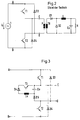
- the basic circuit of a ZTF converter without a switch-off relief network is generally known and e.g. by J.Wüstehube in ELEKTRONIK 1978, number 4, pages 102 to 107, on page 106 as image 9.
- This known ZTF converter circuit is shown in Figure 2.
- the ZTF converter has a transformer TR, the primary winding of which has a first winding connection C and a second winding connection D.
- the first winding connection C is connected via a first power transistor T1 to a first voltage connection A of a voltage source 1, the second winding connection D via a second power transistor T2 to a second voltage connection B of the voltage source 1.
- the first winding connection is also connected to the via a second decoupling diode D4 second voltage terminal B connected; the second winding connection D is connected to the first voltage connection A via a first decoupling diode D3.
- the circuit On the secondary side, the circuit has the arrangement of a rectifier diode D1, a choke coil L, a freewheeling diode D2, an output capacitor Ca and a load resistor R, which is common for a forward converter.
- the transistors T1 and T2 are switched on and off synchronously in the ZTF converter.
- the ZTF converter shown in FIG. 2 is a so-called hard-switching converter, which is only suitable for relatively low switching frequencies because the switching losses place excessive stress on the power transistors at high frequencies. This problem cannot be solved by oversizing the transistors or by connecting transistors in parallel.
- a switch-off relief network which is also referred to below as relief network, can remedy this.
- a DC converter circuit with a relief network is known from DE-PS 24 43 892.
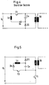
- the circuit of the primary part of a DC-DC converter with a power transistor T1 shown in FIG. 4 can be derived from this.
- a reversing capacitor Cu, a reversing diode Du, a reversing inductance Lu and a decoupling diode D5 are arranged as the switch-off relief network.
- the power transistor T1 is loaded by the ringing current of the relief network.
- the known relief network can also be used for converters with multiple power transistors due to the multiple arrangement. Then there is a relatively high total effort.
- Another DC-DC converter circuit with a relief network is known from DE 27 19 026 A1, a series circuit comprising a diode and a capacitor being connected in parallel with the primary winding of the converter transformer, but the circulating current flows through the power transistor.
- a separate relief network would have to be arranged for each power transistor.
- a two-transistor arrangement with a single relief network is known from JP 2-101 964 A, In .: Patents Abstract of Japan, Sect. E, 1990, Vol. 14, No. 312 (E-948).
- the swinging current flows there via the power transistor Q1.
- swinging around in the event of a short circuit or open circuit cannot be prevented.
- a circuit arrangement with two power transistors and with a relief network is known from DE 36 03 368 A1, with one thyristor being arranged in each relief network for each power transistor.
- the relief networks have a common choke coil.
- the circuit arrangement is only suitable for push-pull operation, i.e. not for the simultaneous operation of two power transistors.
- the invention is based on the object of specifying an improved switch-off relief network.
- a switch-off relief network for a DC / DC converter with at least one clocked power transistor which is connected in series to the primary winding of a transformer, to which the series connection of a diode and a capacitor is connected in parallel, with a swinging diode for the capacitor voltage, the swinging inductance and the Swinging diode is a transistor in series and the series circuit consisting of these three elements is parallel to the capacitor.
- the invention proposes to control the ringing current of the relief network with a separate switch, namely an auxiliary transistor, and not with the Power transistor.
- a separate switch namely an auxiliary transistor
- Such a design of the relief network brings an advantage even in the case of a converter arrangement with a single power transistor, because the power transistor is relieved of the reversing current. It is particularly advantageous to use the relief network in a two-transistor converter, because then both power transistors can be protected with one relief network and a number of components can thus be saved. The savings with other multi-transistor converters are corresponding.
- FIG. 5 shows the primary part of a DC-DC converter with a transformer TR and a power transistor T1.
- the power transistor T1 is connected in series with the primary winding of the transformer TR.
- the intermediate circuit voltage Ui is applied to the series connection.
- the series connection of a reversing capacitor Cu with a decoupling diode D5 is connected in parallel with the primary winding.
- a series connection of a reversing inductance Lu, a reversing diode Du and a transistor T3, also referred to as an auxiliary transistor lies parallel to the reversing capacitor.
- Components with the same function are also provided with the same reference symbols in the other figures of the drawing.
- the additionally required auxiliary transistor T3 is a very small component with a negligibly small power loss.
- the transistor T3 can be switched simultaneously or independently of the transistor T1, as will be explained below using a two-transistor converter.
- FIG. 3 shows the arrangement of the relief network according to the invention in a circuit part of the basic circuit shown in FIG. 2, designated with the connection points AD of a ZTF converter. It can be seen that the two power transistors T1, T2 are protected by a common relief network with the components Du, Lu, Cu and T3 and that only one decoupling diode D5 is required.
- the auxiliary transistor T3 can be switched on and off together with the power transistors T1 and T2. However, it can also be provided with its own driver circuit and switched on and off at times other than the power transistors T1 and T2.
- auxiliary transistor T3 By suitable control of the auxiliary transistor T3 it can be achieved that the auxiliary transistor T3 with a very small duty cycle, e.g. does not switch on in the event of an open circuit or short circuit. An idle or short-circuit protection can thus be achieved.
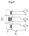
- a suitable circuit arrangement for driving the auxiliary transistor T3 is shown in FIG. In this arrangement, the power transistors T1 and T2 and the auxiliary transistor T3 are controlled via separate secondary windings of a drive transformer 2. The auxiliary transistor T3 is connected to one of the secondary windings with the interposition of a signal transistor T4.
- the signal transistor T4 blocks when the pulse duty factor becomes smaller than tu / TS (see FIG. 10).
- the relief network according to FIG. 3 can be designed such that after the power transistors T1 and T2 are switched off, the switch-off losses become very small, but the voltage at the reversing capacitor Cu reaches the value of the intermediate circuit voltage Ui after a short time.
- the demagnetizing diodes D3 and D4 then become conductive and the decoupling diode D5 blocks.
- the auxiliary transistor T3 can be switched on again at this point in time, as a result of which the oscillation takes place. This has the advantage that switch the power transistors T1, T2 (when using bipolar transistors or IGBTs) at a voltage at the transistor of approximately zero volts and thus there are no switch-on losses.
- the demagnetizing diodes D3 and D4 remain in the circuit, the blocking voltages at the power transistors T1 and T2 are defined in an upper limit, specifically to the value of the intermediate circuit voltage Ui. This can be taken into account when designing the safety reserve for the permissible reverse voltage of the transistors T1 and T2.
- the demagnetization time of the transformer is slightly increased if the diodes D3 and D4 remain in the circuit. However, this is not a disadvantage, since the demagnetizing energy of the transformer TR can be used regeneratively to supply the load, which results in a reduction in the switching time of the transistors T1, T2.
- An additional saturable small inductance can be connected in series with the reversing inductance Lu, which can be advantageous for the recovery behavior of the reversing diode Du.
- Zener diodes can be connected in series with the demagnetizing diodes D3, D4. Such an arrangement has the advantage that the demagnetization of the transformer TR takes place with a higher voltage and consequently the demagnetization is completed in a shorter time. The Zener diodes also ensure that the voltage time areas are equal.
- FIG. 1 shows the application of the circuit part shown in FIG. 3 in the two-transistor flow converter circuit indicated as the basic circuit in FIG. Idealized components are assumed in the overall circuit according to FIG. 1. A functional description is given below using this circuit.
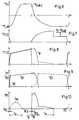
- FIG. 6 The current and voltage arrows required for explanation are entered in FIG.
- the current and voltage profiles of some currents and voltages are shown in FIGS. 6 to 10.
- the reversing capacitor Cu becomes effective as a voltage source.
- the current through the two power transistors T1 and T2 commutates to the branch consisting of the reversing capacitor Cu and diode D5.
- the current iP (t) in the primary winding P remains almost unaffected by this commutation, which takes place very quickly.
- the further time course of the current iP (t) and thus also the currents iD1 (t) and iD2 (t) is now determined by the reversing capacitor Cu.
- the load circuit now acts like a constant current source that linearly discharges the reversing capacitor Cu.
- an oscillation is superimposed, the characteristic frequency of which is composed of the transformer main and leakage inductance, the parasitic inductances of the primary circuit and the reversing capacitor Cu.
- the diode D2 becomes conductive.
- the load circuit is now separated from the primary circuit.
- the transformer TR is demagnetized. If uCu (t) does not reach the value of the intermediate circuit voltage Ui, the two demagnetizing diodes remain ineffective.
- the entire magnetizing energy of the transformer, the primary parasitic inductances and leakage inductance of the transformer is now in the form of a charge in the reversing capacitor Cu, which is released to the load circuit in the next switching cycle.
- FIGS. 6 to 10 show the case in which the demagnetizing diodes D3 and D4 do not become conductive.
- the voltage uCu (t) can assume values greater than the magnitude of the intermediate circuit voltage. In this case, the demagnetization of the transformer is faster. However, the power transistors are loaded with higher reverse voltages.
- the blocking voltages at the two power transistors T1 and T2 reach their maximum value in this switching interval.
Abstract
Description
Die Erfindung bezieht sich auf ein Ausschaltentlastungsnetzwerk zur Verringerung der Schaltverluste eines oder mehrerer Leistungstransistoren in einem Gleichspannungswandler.The invention relates to a switch-off relief network for reducing the switching losses of one or more power transistors in a DC converter.
Das erfindungsgemäße Ausschaltentlastungsnetzwerk wird hauptsächlich am Beispiel eines Zwei-Transistor-Fluß(ZTF)-Konverters erläutert. Es ist jedoch auch für einen Gleichspannungswandler mit einem einzigen Leistungstransistor oder für Konverterschaltungen mit mehr als zwei Transistoren sinngemäß anwendbar. Gleichspannungswandler mit einem einzigen Leistungstransistor sind z.B. als Sperrwandler oder als Sperr-Flußkonverter bekannt. Beim Sperr-Flußkonverter ist in Reihe zur Primärwicklung des Flußkonvertertransformators die Primärwicklung eines Sperrwandlertransformators geschaltet. Der Flußkonvertertransformator überträgt Energie, solange der Leistungsschalter eingeschaltet ist. Gleichzeitig wird durch die Reihenschaltung mit dem Sperrwandlertransformator dieser aufmagnetisiert. Sobald der Leistungsschalter ausgeschaltet wird, übernimmt der Sperrwandlertransformator sekundärseitig die weitere Speisung der Last, da die Magnetisierungsenergie des Sperrwandlertransformators wieder abgebaut werden muß.The switch-off relief network according to the invention is mainly explained using the example of a two-transistor flux (ZTF) converter. However, it can also be used analogously for a DC / DC converter with a single power transistor or for converter circuits with more than two transistors. DC-DC converters with a single power transistor are known, for example, as flyback converters or as flyback flux converters. In the reverse flux converter, the primary winding of a flyback transformer is connected in series with the primary winding of the flux converter transformer. The flux converter transformer transmits energy as long as the circuit breaker is on. At the same time, the series connection with the flyback transformer transforms this magnetized. As soon as the circuit breaker is switched off, the flyback transformer takes over the further supply of the Load, since the magnetizing energy of the flyback transformer has to be reduced again.
Die Grundschaltung eines ZTF-Konverters ohne Ausschaltentlastungsnetzwerk ist allgemein bekannt und z.B. von J.Wüstehube in ELEKTRONIK 1978, Heft 4, Seiten 102 bis 107, auf Seite 106 als Bild 9 angegeben. Diese bekannte ZTF-Konverterschaltung ist in Figur 2 wiedergegeben. Der ZTF-Konverter weist einen Transformator TR auf, dessen Primärwicklung einen ersten Wicklungsanschluß C und einen zweiten Wicklungsanschluß D hat. Der erste Wicklungsanschluß C ist über einen ersten Leistungstransistor T1 mit einem ersten Spannungsanschluß A einer Spannungsquelle 1 verbunden, der zweite Wicklungsanschluß D über einen zweiten Leistungstransistor T2 mit einem zweiten Spannungsanschluß B der Spannungsquelle 1. Der erste Wicklungsanschluß ist außerdem über eine zweite Entkopplungsdiode D4 mit dem zweiten Spannungsanschluß B verbunden; der zweite Wicklungsanschluß D ist über eine erste Entkopplungsdiode D3 mit dem ersten Spannungsanschluß A verbunden. Sekundärseitig weist die Schaltung die für einen Durchflußwandler übliche Anordnung einer Gleichrichterdiode D1, einer Drosselspule L, einer Freilaufdiode D2, eines Ausgangskondensators Ca und eines Lastwiderstands R auf.The basic circuit of a ZTF converter without a switch-off relief network is generally known and e.g. by J.Wüstehube in ELEKTRONIK 1978, number 4,
Die Transistoren T1 und T2 werden beim ZTF-Konverter synchron ein- und ausgeschaltet. Der in Figur 2 dargestellte ZTF-Konverter ist ein sogenannter hart-schaltender Konverter, der nur für relativ niedrige Schaltfrequenzen geeignet ist, weil die Schaltverluste die Leistungstransistoren bei hohen Frequenz zu stark belasten. Dieses Problem läßt sich nicht durch Überdimensionieren der Transistoren oder durch Parallelschalten von Transistoren lösen. Abhilfe kann ein Ausschaltentlastungsnetzwerk schaffen, das nachstehend auch mit Entlastungsnetzwerk bezeichnet ist.The transistors T1 and T2 are switched on and off synchronously in the ZTF converter. The ZTF converter shown in FIG. 2 is a so-called hard-switching converter, which is only suitable for relatively low switching frequencies because the switching losses place excessive stress on the power transistors at high frequencies. This problem cannot be solved by oversizing the transistors or by connecting transistors in parallel. A switch-off relief network, which is also referred to below as relief network, can remedy this.
Eine Gleichspannungswandlerschaltung mit Entlastungsnetzwerk ist aus der DE-PS 24 43 892 bekannt. Daraus läßt sich die in Figur 4 angegebene Schaltung des Primärteils eines Gleichspannungswandlers mit einem Leistungstransistor T1 ableiten. Als Ausschaltentlastungsnetzwerk sind ein Umschwingkondensator Cu, eine Umschwingdiode Du, eine Umschwinginduktivität Lu und eine Entkopplungsdiode D5 angeordnet. Allerdings wird bei dieser Schaltungsanordnung der Leistungstransistor T1 durch den Umschwingstrom des Entlastungsnetzwerkes belastet. Das bekannte Entlastungsnetzwerk läßt sich im Prinzip durch Mehrfachanordnung auch für Konverter mit mehreren Leistungstransistoren anwenden. Dann ergibt sich aber ein relativ hoher Gesamtaufwand.A DC converter circuit with a relief network is known from DE-PS 24 43 892. The circuit of the primary part of a DC-DC converter with a power transistor T1 shown in FIG. 4 can be derived from this. A reversing capacitor Cu, a reversing diode Du, a reversing inductance Lu and a decoupling diode D5 are arranged as the switch-off relief network. In this circuit arrangement, however, the power transistor T1 is loaded by the ringing current of the relief network. In principle, the known relief network can also be used for converters with multiple power transistors due to the multiple arrangement. Then there is a relatively high total effort.
Eine weitere Gleichspannungswandlerschaltung mit Entlastungsnetzwerk ist aus der DE 27 19 026 A1 bekannt, wobei eine Reihenschaltung aus einer Diode und einem Kondensator parallel zur Primärwicklung des Wandlertransformators geschaltet ist, allerdings der Umschwingstrom über den Leistungstransistor fließt. Außerdem müßte auch bei dieser bekannten Anordnung im Fall einer Mehr-Transistor-Anordnung für jeden Leistungstransistor ein gesondertes Entlastungsnetzwerk angeordnet werden.Another DC-DC converter circuit with a relief network is known from DE 27 19 026 A1, a series circuit comprising a diode and a capacitor being connected in parallel with the primary winding of the converter transformer, but the circulating current flows through the power transistor. In addition, with this known arrangement, in the case of a multi-transistor arrangement, a separate relief network would have to be arranged for each power transistor.
Eine Zwei-Transistor-Anordnung mit einem einzigen Entlastungsnetzwerk ist aus JP 2-101 964 A, In.: Patents Abstract of Japan, Sect. E, 1990, Vol. 14, Nr. 312 (E-948) bekannt. Der Umschwingstrom fließt dort über den Leistungstransistor Q1. Wie bei allen vorgenannten Schaltungen, kann das Umschwingen im Kurzschluß- oder Leerlauffall auch nicht unterbunden werden.A two-transistor arrangement with a single relief network is known from JP 2-101 964 A, In .: Patents Abstract of Japan, Sect. E, 1990, Vol. 14, No. 312 (E-948). The swinging current flows there via the power transistor Q1. As with all of the circuits mentioned above, swinging around in the event of a short circuit or open circuit cannot be prevented.
Aus JP 58-69 463 A, In.: Patents Abstract of Japan, Sect. E, Vol. 7, 1983, Nr. 162 (E-187) ist eine weitere, aufwendige Schaltungsanordnung mit einem Hilfstransistor bekannt, der über eine Hilfswicklung am Transformator angesteuert wird. Bei dieser Schaltungsanordnung wird die Gleichspannungsquelle in nachteiliger Weise mit dem Umschwingstrom und Entmangetisierungsströmen belastet, also mit impulsförmigen Strömen.From JP 58-69 463 A, In .: Patents Abstract of Japan, Sect. E, Vol. 7, 1983, No. 162 (E-187) a further, complex circuit arrangement with an auxiliary transistor is known, which is controlled via an auxiliary winding on the transformer. With this circuit arrangement the DC voltage source adversely burdened with the reversing current and demanganizing currents, that is, with pulsed currents.
Eine Schaltungsanordnung mit zwei Leistungstransistoren und mit Entlastungsnetzwerk ist aus der DE 36 03 368 A1 bekannt, wobei je Leistungstransistor ein Thyristor in jedem Entlastungsnetzwerk angeordnet ist. Die Entlastungsnetzwerke weisen eine gemeinsame Drosselspule auf. DIe Schaltungsanordnung ist nur für Gegentaktbetrieb, also nicht für den Simultanbetrieb von zwei Leistungstransistoren geeignet.A circuit arrangement with two power transistors and with a relief network is known from DE 36 03 368 A1, with one thyristor being arranged in each relief network for each power transistor. The relief networks have a common choke coil. The circuit arrangement is only suitable for push-pull operation, i.e. not for the simultaneous operation of two power transistors.
Ausgehend von dem aus der DE 27 19 026 A1 bekannten Stand der Technik liegt der Erfindung die Aufgabe zugrunde, ein verbessertes Ausschaltentlastungsnetzwerk anzugeben.Starting from the prior art known from DE 27 19 026 A1, the invention is based on the object of specifying an improved switch-off relief network.
Diese Aufgabe wird gelöst durch ein Ausschaltentlastungsnetzwerk für einen Gleichspannungswandler mit wenigstens einem getakteten Leistungstransistor, der in Reihe zur Primärwicklung eines Transformators liegt, zu welcher die Reihenschaltung einer Diode und eines Kondensators parallel liegt, mit einer Umschwingdiode für die Kondensatorspannung, wobei zu der Umschwinginduktivität und der Umschwingdiode ein Transistor in Reihe liegt und die aus diesen drei Elementen bestehende Reihenschaltung zum Kondensator parallel liegt.This object is achieved by a switch-off relief network for a DC / DC converter with at least one clocked power transistor which is connected in series to the primary winding of a transformer, to which the series connection of a diode and a capacitor is connected in parallel, with a swinging diode for the capacitor voltage, the swinging inductance and the Swinging diode is a transistor in series and the series circuit consisting of these three elements is parallel to the capacitor.
Ausgestaltungen und Vorteile der Erfindung sind der nachstehenden Erläuterung anhand der Figuren der Zeichnung zu entnehmen.Embodiments and advantages of the invention can be found in the following explanation with reference to the figures of the drawing.
Es zeigen:
- Figur 1
- Zwei-Transistor-Fluß(ZTF)-Konverterschaltung mit Ausschaltentlastungsnetzwerk,
Figur 2- ZTF-Konverter nach dem Stand der Technik (ohne Entlastungsnetzwerk),
- Figur 3
- erfindungsgemäßes Ausschaltentlastungsnetzwerk in einer Anordnung mit zwei Leistungstransistoren,
- Figur 4
- Teil eines Gleichspannungswandlers mit Ausschaltentlastungsnetzwerk nach dem Stand der Technik,
Figur 5- Teil eines Gleichspannungswandlers mit erfindungsgemäßem Ausschaltentlastungsnetzwerk,
- Figur 6 bis 10
- Spannungs- und Stromverläufe in der Konverteranordnung nach Figur 1, wobei
- Figur 6
- den Spannungsverlauf am Umschwingkondensator zeigt,
- Figur 7
- den Spannungsverlauf an den Leistungstransistoren,
- Figur 8
- den Stromverlauf in den Leistungstransistoren und den Primärstrom des Transformators,
- Figur 9
- den Stromverlauf in der Gleichrichterdiode und der Freilaufdiode, und
- Figur 10
- den Stromverlauf in der Entkopplungsdiode und der Umschwingdiode,
Figur 11- eine Ansteueranordnung.
- Figure 1
- Two-transistor flux (ZTF) converter circuit with switch-off relief network,
- Figure 2
- ZTF converter according to the state of the art (without relief network),
- Figure 3
- switch-off relief network according to the invention in an arrangement with two power transistors,
- Figure 4
- Part of a DC-DC converter with switch-off relief network according to the prior art,
- Figure 5
- Part of a DC-DC converter with switch-off relief network according to the invention,
- Figure 6 to 10
- Voltage and current profiles in the converter arrangement according to Figure 1, wherein
- Figure 6
- shows the voltage curve at the reversing capacitor,
- Figure 7
- the voltage curve at the power transistors,
- Figure 8
- the current profile in the power transistors and the primary current of the transformer,
- Figure 9
- the current profile in the rectifier diode and the freewheeling diode, and
- Figure 10
- the current profile in the decoupling diode and the swinging diode,
- Figure 11
- a control arrangement.
Mit der Erfindung wird vorgeschlagen, den Umschwingstrom des Entlastungsnetzwerkes mit einem separaten Schalter, nämlich einem Hilfstransistor, zu steuern und nicht mit dem Leistungstransistor. Eine solche Gestaltung des Entlastungsnetzwerkes bringt selbst bei einer Konverteranordnung mit einem einzigen Leistungstransistor einen Vorteil, weil der Leistungstransistor vom Umschwingstrom entlastet wird. Besonders vorteilhaft ist die Verwendung des Entlastungsnetzwerkes in einem Zwei-Transistor-Konverter, weil dann mit einem Entlastungsnetzwerk beide Leistungstransistoren geschützt werden können und somit eine Reihe von Bauelementen eingespart werden können. Entsprechend ist die Einsparung bei sonstigen Mehrtransistorkonvertern.The invention proposes to control the ringing current of the relief network with a separate switch, namely an auxiliary transistor, and not with the Power transistor. Such a design of the relief network brings an advantage even in the case of a converter arrangement with a single power transistor, because the power transistor is relieved of the reversing current. It is particularly advantageous to use the relief network in a two-transistor converter, because then both power transistors can be protected with one relief network and a number of components can thus be saved. The savings with other multi-transistor converters are corresponding.
Figur 5 zeigt den Primärteil eines Gleichspannungswandlers mit einem Transformator TR und einem Leistungstransistor T1. Der Leistungstransistor T1 ist in Reihe zur Primärwicklung des Trnsformators TR geschaltet. An die Reihenschaltung ist die Zwischenkreisspannung Ui angelegt. Parallel zur Primärwicklung ist die Reihenschaltung eines Umschwingkondensators Cu mit einer Entkopplungsdiode D5 geschaltet. Ausgehend vom Verbindungspunkt zwischen dem Umschwingkondensator Cu und der Entkopplungsdiode D5 liegt eine Reihenschaltung einer Umschwinginduktivität Lu, einer Umschwingdiode Du und eines auch als Hilfstransistor bezeichneten Transistors T3 parallel zum Umschwingkondensator. Bauelemente mit übereinstimmender Funktion sind auch in den anderen Figuren der Zeichnung mit den gleichen Bezugszeichen versehen.FIG. 5 shows the primary part of a DC-DC converter with a transformer TR and a power transistor T1. The power transistor T1 is connected in series with the primary winding of the transformer TR. The intermediate circuit voltage Ui is applied to the series connection. The series connection of a reversing capacitor Cu with a decoupling diode D5 is connected in parallel with the primary winding. Starting from the connection point between the reversing capacitor Cu and the decoupling diode D5, a series connection of a reversing inductance Lu, a reversing diode Du and a transistor T3, also referred to as an auxiliary transistor, lies parallel to the reversing capacitor. Components with the same function are also provided with the same reference symbols in the other figures of the drawing.
Der zusätzlich erforderliche Hilfstransistor T3 ist ein sehr kleines Bauteil mit einer vernachlässigbar kleinen Verlustleistung. Der Transistor T3 kann gleichzeitig oder unabhängig vom Transistor T1 geschaltet werden, wie nachstehend anhand eines Zwei-Transistor-Konverters erläutert wird.The additionally required auxiliary transistor T3 is a very small component with a negligibly small power loss. The transistor T3 can be switched simultaneously or independently of the transistor T1, as will be explained below using a two-transistor converter.
Figur 3 zeigt die Anordnung des erfindungsgemäßen Entlastungsnetzwerkes in einem mit den Anschlußstellen A-D bezeichneten Schaltungsteil der in Figur 2 gezeigten Grundschaltung eines ZTF-Konverters. Es ist zu erkennen, daß die beiden Leistungstransistoren T1, T2 durch ein gemeinsames Entlastungsnetzwerk mit den Komponenten Du, Lu, Cu und T3 geschützt werden und daß nur eine Entkopplungsdiode D5 erforderlich ist.FIG. 3 shows the arrangement of the relief network according to the invention in a circuit part of the basic circuit shown in FIG. 2, designated with the connection points AD of a ZTF converter. It can be seen that the two power transistors T1, T2 are protected by a common relief network with the components Du, Lu, Cu and T3 and that only one decoupling diode D5 is required.
Der Hilfstransistor T3 kann gemeinsam mit den Leistungstransistoren T1 und T2 ein- und ausgeschaltet werden. Er kann aber auch mit einer eigenen Treiberschaltung versehen werden und zu anderen Zeiten als die Leistungstransistoren T1 und T2 ein- und ausgeschaltet werden.The auxiliary transistor T3 can be switched on and off together with the power transistors T1 and T2. However, it can also be provided with its own driver circuit and switched on and off at times other than the power transistors T1 and T2.
Durch geeignete Ansteuerung des Hilfstransistors T3 kann erreicht werden, daß der Hilfstransistor T3 bei sehr kleinem Tastverhältnis, z.B. im Leerlauf- oder Kurzschlußfall, nicht einschaltet. Es kann somit eine Leerlauf- oder Kurzschlußsicherung erreicht werden. Eine geeignete Schaltungsanordnung zur Ansteuerung des Hilfstransistors T3 ist in Figur 11 dargestellt. Die Leistungstransistoren T1 und T2 und der Hilfstransistor T3 werden bei dieser Anordnung über getrennte Sekundärwicklungen eines Ansteuerübertragers 2 gesteuert. Der Anschluß des Hilfstransistors T3 an eine der Sekundärwicklungen erfolgt unter Zwischenschaltung eines Signaltransistors T4.By suitable control of the auxiliary transistor T3 it can be achieved that the auxiliary transistor T3 with a very small duty cycle, e.g. does not switch on in the event of an open circuit or short circuit. An idle or short-circuit protection can thus be achieved. A suitable circuit arrangement for driving the auxiliary transistor T3 is shown in FIG. In this arrangement, the power transistors T1 and T2 and the auxiliary transistor T3 are controlled via separate secondary windings of a
Der Signaltransistor T4 sperrt, wenn das Tastverhältnis kleiner als tu/TS wird (vergl. Figur 10).The signal transistor T4 blocks when the pulse duty factor becomes smaller than tu / TS (see FIG. 10).
Das Entlastungsnetzwerk gemäß Figur 3 kann so ausgelegt werden, daß nach dem Ausschalten der Leistungstransistoren T1 und T2 die Ausschaltverluste sehr klein werden, die Spannung am Umschwingkondensator Cu aber nach kurzer Zeit den Wert der Zwischenkreisspannung Ui erreicht. Die Entmagnetisierungs-Dioden D3 und D4 werden dann leitend und die Entkopplungsdiode D5 sperrt. Der Hilfstransistor T3 kann bereits zu diesem Zeitpunkt wieder eingeschaltet werden, wodurch das Umschwingen erfolgt. Das hat den Vorteil, daß die Leistungstransistoren T1, T2 (bei Verwendung von bipolaren Transistoren oder IGBTs) bei einer Spannung am Transistor von etwa Null Volt schalten und somit keine Einschaltverluste entstehen.The relief network according to FIG. 3 can be designed such that after the power transistors T1 and T2 are switched off, the switch-off losses become very small, but the voltage at the reversing capacitor Cu reaches the value of the intermediate circuit voltage Ui after a short time. The demagnetizing diodes D3 and D4 then become conductive and the decoupling diode D5 blocks. The auxiliary transistor T3 can be switched on again at this point in time, as a result of which the oscillation takes place. This has the advantage that switch the power transistors T1, T2 (when using bipolar transistors or IGBTs) at a voltage at the transistor of approximately zero volts and thus there are no switch-on losses.
Es ist anzumerken, daß durch ein Verbleiben der Entmagnetisierungsdioden D3 und D4 in der Schaltung die Sperrspannungen an den Leistungstransistoren T1 und T2 definiert nach oben begrenzt werden, und zwar auf den Wert der Zwischenkreisspannung Ui. Dies kann bei der Auslegung der Sicherheitsreserve für die zulässige Sperrspannung der Transistoren T1 und T2 berücksichtigt werden. Allerdings wird die Entmagnetisierungszeit des Transformators geringfügig verlängert, wenn die Dioden D3 und D4 in der Schaltung verbleiben. Dies ist aber kein Nachteil, da sich die Entmagnetisierungsenergie des Transformators TR regenerativ zur Speisung der Last einsetzen läßt, wodurch sich eine Reduzierung der Umschaltzeit der Transistoren T1, T2 ergibt.It should be noted that if the demagnetizing diodes D3 and D4 remain in the circuit, the blocking voltages at the power transistors T1 and T2 are defined in an upper limit, specifically to the value of the intermediate circuit voltage Ui. This can be taken into account when designing the safety reserve for the permissible reverse voltage of the transistors T1 and T2. However, the demagnetization time of the transformer is slightly increased if the diodes D3 and D4 remain in the circuit. However, this is not a disadvantage, since the demagnetizing energy of the transformer TR can be used regeneratively to supply the load, which results in a reduction in the switching time of the transistors T1, T2.
In Reihe zur Umschwinginduktivität Lu kann eine zusätzliche sättigbare kleine Induktivität geschaltet werden, was bei dem Recovery-Verhalten der Umschwingdiode Du von Vorteil sein kann.An additional saturable small inductance can be connected in series with the reversing inductance Lu, which can be advantageous for the recovery behavior of the reversing diode Du.
Weiterhin ist anzumerken, daß in Reihe zu den Entmagnetisierungsdioden D3, D4 zusätzlich Zenerdioden (in der Zeichnung nicht dargestellt) geschaltet werden können. Eine solche Anordnung hat den Vorteil, daß die Entmagnetisierung des Transformators TR mit einer höheren Spannung erfolgt und demzufolge die Entmagnetisierung in einer kürzeren Zeit abgeschlossen ist. Die Zenerdioden stellen auch eine Gleichheit der Spannungszeitflächen sicher.It should also be noted that Zener diodes (not shown in the drawing) can be connected in series with the demagnetizing diodes D3, D4. Such an arrangement has the advantage that the demagnetization of the transformer TR takes place with a higher voltage and consequently the demagnetization is completed in a shorter time. The Zener diodes also ensure that the voltage time areas are equal.
Figur 1 zeigt die Anwendung des in Figur 3 gezeigten Schaltungsteils in der in Figur 2 als Grundschaltung angegebenen Zwei-Transistor-Flußkonverterschaltung. In der Gesamtschaltung nach Figur 1 sind idealisierte Bauelemente angenommen. Anhand dieser Schaltung erfolgt nachstehend eine Funktionsbeschreibung.FIG. 1 shows the application of the circuit part shown in FIG. 3 in the two-transistor flow converter circuit indicated as the basic circuit in FIG. Idealized components are assumed in the overall circuit according to FIG. 1. A functional description is given below using this circuit.
In Figur 1 sind die zur Erläuterung erforderlichen Strom- und Spannungspfeile eingetragen. Die Strom- und Spannungsverläufe von einigen Strömen und Spannungen sind in den Figuren 6 bis 10 dargestellt. Die Funktionsbeschreibung für den eingeschwungenen Zustand beginnt in einem Zeitpunkt t=0, wenn die drei Transistoren T1, T2 und T3 eingeschaltet werden (d.h. die Ansteuerung erfolgt mit einer gemeinsamen Treiberschaltung) und endet zu einem Zeitpunkt t=TS, wobei TS die Schaltperiodendauer ist. Die Spannung uCu(t) am Umschwingkondensator Cu wird zum Zeitpunkt t=0 gesetzt als uCu(t=0)=-UCuO, deren Betrag kleiner oder gleich ist dem Betrag der Zwischenkreisspannung Ui (vergleiche Figur 6; die angesprochenen Zeitpunkte t sind jeweils aus Figur 10 ersichtlich).The current and voltage arrows required for explanation are entered in FIG. The current and voltage profiles of some currents and voltages are shown in FIGS. 6 to 10. The functional description for the steady state begins at a point in time t = 0 when the three transistors T1, T2 and T3 are switched on (i.e. they are driven by a common driver circuit) and ends at a point in time t = TS, where TS is the switching period. The voltage uCu (t) at the reversing capacitor Cu is set at the time t = 0 as uCu (t = 0) = - UCuO, the amount of which is less than or equal to the amount of the intermediate circuit voltage Ui (see FIG. 6; the times t mentioned are each off Figure 10 can be seen).
Nachdem die Leistungstransistoren T1 und T2 eingeschaltet worden sind, kommutiert der Laststrom von Diode D2 nach Diode D1 bis zu einem Zeitpunkt t=tk1 der Strom durch die Diode D2 iD2(t=tk1)=0 beträgt (vergleiche Figur 9). Gleichzeitig schwingt durch das Schließen des Hilfstransistors T3 die Ladung des Umschwingkondensators Cu über die Umschwinginduktivität Lu sinusförmig um, bis zum Zeitpunkt t=tu der Umschwingstrom wieder den Wert Null erreicht (vergleiche iDu-Verlauf in Figur 10). Zu einem Ausschaltzeitpunkt t=tA werden die Transistoren T1, T2 und T3 wieder ausgeschaltet. Erreicht die Spannung uP(t) an der Primärwicklung P den Wert der Kondensatorspannung, also up(t)=UCuU wird der Umschwingkondensator Cu als Spannungsquelle wirksam. Der Strom durch die beiden Leistungstransistoren T1 und T2 kommutiert auf den aus Umschwingkondensator Cu und Diode D5 bestehenden Zweig. Der Strom iP(t) in der Primärwicklung P bleibt von dieser Kommutierung, die sehr schnell abläuft, nahezu unbeeinflußt. Die Spannungen an den beiden Leistungstransistoren T1 und T2 (vergleiche Figur 7) nehmen die Differenz von Zwischenkreisspannung Ui und Umschwingkondensatorspannung UCu an. Diese Kommutierung ist beendet, wenn nach der Zeit t=tk2 die Ströme durch T1 und T2 Null werden (vergleiche Figur 8).After the power transistors T1 and T2 have been switched on, the load current commutates from diode D2 to diode D1 until the time through the diode D2 iD2 (t = tk1) = 0 until a time t = tk1 (see FIG. 9). At the same time, the closing of the auxiliary transistor T3 causes the charge on the reversing capacitor Cu to oscillate sinusoidally via the reversing inductance Lu, until the reversing current reaches zero again at time t = tu (see iDu curve in FIG. 10). At a switch-off instant t = tA, the transistors T1, T2 and T3 are switched off again. If the voltage uP (t) at the primary winding P reaches the value of the capacitor voltage, ie up (t) = UCuU, the reversing capacitor Cu becomes effective as a voltage source. The current through the two power transistors T1 and T2 commutates to the branch consisting of the reversing capacitor Cu and diode D5. The current iP (t) in the primary winding P remains almost unaffected by this commutation, which takes place very quickly. Take the voltages at the two power transistors T1 and T2 (see Figure 7) the difference between the intermediate circuit voltage Ui and the swinging capacitor voltage UCu. This commutation is ended when after the time t = tk2 the currents through T1 and T2 become zero (see FIG. 8).
Der weitere zeitliche Verlauf des Stromes iP(t) und damit auch der Ströme iD1(t) und iD2(t) wird jetzt durch den Umschwingkondensator Cu bestimmt. Der Lastkreis wirkt jetzt quasi wie eine Konstantstromquelle, die den Umschwingkondensator Cu linear entlädt. Zudem überlagert sich eine Schwingung, deren Kennkreisfrequenz sich aus Transformator Haupt- und Streuinduktivität, den parasitären Induktivitäten des Primärkreises und des Umschwingkondensators Cu zusammensetzt.The further time course of the current iP (t) and thus also the currents iD1 (t) and iD2 (t) is now determined by the reversing capacitor Cu. The load circuit now acts like a constant current source that linearly discharges the reversing capacitor Cu. In addition, an oscillation is superimposed, the characteristic frequency of which is composed of the transformer main and leakage inductance, the parasitic inductances of the primary circuit and the reversing capacitor Cu.
Wenn nach der Zeit t=tN, also der Nachladephase die Spannung an der Diode D2 den Wert der Durchlaßspannung unterschreitet, wird die Diode D2 leitend. Der Laststrom kommutiert nach Cosinus- und Sinusfunktionen von Diode D1 auf Diode D2, bis nach der Zeit t=tk3 der Strom iD2(t=Tk3) den Wert des Laststromes erreicht (vergleiche Figur 9).If after the time t = tN, that is to say the recharging phase, the voltage on the diode D2 falls below the value of the forward voltage, the diode D2 becomes conductive. The load current commutates according to cosine and sine functions from diode D1 to diode D2 until after the time t = tk3 the current iD2 (t = Tk3) reaches the value of the load current (see FIG. 9).
Der Lastkreis ist jetzt vom Primärkreis getrennt. Im weiteren Verlauf wird der Transformator TR entmagnetisiert. Erreicht uCu(t) nicht den Wert der Zwischenkreisspannung Ui, bleiben die beiden Entmagnetisierungsedioden unwirksam. Die gesamte Magnetisierungsenergie des Transformators, der primärseitigen parasitären Induktivitäten und Streuinduktivität des Transformators befindet sich jetzt als Ladung im Umschwingkondensator Cu, die im nächsten Schaltzyklus an den Lastkreis abgegeben wird.The load circuit is now separated from the primary circuit. In the further course, the transformer TR is demagnetized. If uCu (t) does not reach the value of the intermediate circuit voltage Ui, the two demagnetizing diodes remain ineffective. The entire magnetizing energy of the transformer, the primary parasitic inductances and leakage inductance of the transformer is now in the form of a charge in the reversing capacitor Cu, which is released to the load circuit in the next switching cycle.
Erreicht die Spannung uCu(t) am Kondensator Cu den Wert der Zwischenkreisspannung Ui, werden die Dioden D3 und D4 leitend. Die restliche, im Transformator noch enthaltene Magnetisierungsenergie wird in den Zwischenkreis zurückgespeist.If the voltage uCu (t) at the capacitor Cu reaches the value of the intermediate circuit voltage Ui, the diodes D3 and D4 become conductive. The remaining magnetization energy still contained in the transformer is fed back into the intermediate circuit.
In den Figuren 6 bis 10 ist der Fall, daß die Entmagnetisierungsdioden D3 und D4 nicht leitend werden, eingezeichnet.FIGS. 6 to 10 show the case in which the demagnetizing diodes D3 and D4 do not become conductive.
Sind die Entmagnetisierungsdioden D3 und D4 nicht vorhanden, kann die Spannung uCu(t) größere Werte als den Betrag der Zwischenkreisspannung annehmen. Die Entmagnetisierung des Transformators erfolgt in diesem Fall schneller. Allerdings werden die Leistungstransistoren mit höheren Sperrspannungen belastet.If the demagnetizing diodes D3 and D4 are not present, the voltage uCu (t) can assume values greater than the magnitude of the intermediate circuit voltage. In this case, the demagnetization of the transformer is faster. However, the power transistors are loaded with higher reverse voltages.
Ist die Entmagnetisierung des Transformators nach der Entmagnetisierungszeit t=te abgeschlossen oder werden die Dioden D3 und D4 leitend, sperrt die Diode D5, und der Umschwingkondensator Cu bleibt auf der jetzt erreichten negativen Spannung, also uCu(t=te)=-UCu0 aufgeladen.If the demagnetization of the transformer is completed after the demagnetization time t = te or the diodes D3 and D4 become conductive, the diode D5 blocks and the reversing capacitor Cu remains charged to the negative voltage now reached, i.e. uCu (t = te) = - UCu0.
Die Sperrspannungen an den beiden Leistungstransistoren T1 und T2 erreichen in diesem Schaltintervall ihren maximalen Wert.The blocking voltages at the two power transistors T1 and T2 reach their maximum value in this switching interval.
Nachdem der Transformator entmagnetisiert ist, laufen primärseitig bei idealen Bauelementen keinerlei Schwingvorgänge ab. Die Sperrspannungen an den Transistoren T1 und T2 verringern sich auf das Niveau der halben Zwischenkreisspannung, wie auch beim ZTF-Konverter ohne das Entlastungsnetzwerk (uP(t)=0). An der Diode D5 liegt als Sperrspannung die Spannung des Umschwingkondensators Cu an. Die Leistungstransistoren T1 und T2 können jetzt wieder eingeschaltet werden.After the transformer is demagnetized, no vibrations occur on the primary side with ideal components. The blocking voltages at the transistors T1 and T2 decrease to the level of half the intermediate circuit voltage, as also with the ZTF converter without the relief network (uP (t) = 0). The voltage of the reversing capacitor Cu is present as the reverse voltage at the diode D5. The power transistors T1 and T2 can now be switched on again.
- 11
- Spannungsquelle für Zwischenkreisspannung (Ui)Voltage source for DC link voltage (Ui)
- 22nd
- AnsteuerübertragerControl transformer
- AA
- erster Spannungsanschlußfirst voltage connection
- BB
- zweiter Spannungsanschlußsecond voltage connection
- CC.
- erster Wicklungsanschlußfirst winding connection
- CaApprox
- AusgangskondensatorOutput capacitor
- CuCu
- UmschwingkondensatorSwinging capacitor
- DD
- zweiter Wicklungsanschlußsecond winding connection
- D1D1
- GleichrichterdiodeRectifier diode
- D2D2
- FreilaufdiodeFree-wheeling diode
- D3D3
- erste Entmagnetisierungsdiodefirst demagnetizing diode
- D4D4
- zweite Entmagnetisierungsdiodesecond demagnetizing diode
- D5D5
- erste Entkopplungsdiodefirst decoupling diode
- DuYou
- UmschwingdiodeSwinging diode
- LuLu
- UmschwinginduktivitätSwinging inductance
- PP
- PrimärwicklungPrimary winding
- RR
- LastwiderstandLoad resistance
- T1T1
- erster Leistungstransistorfirst power transistor
- T2T2
- zweiter Leistungstransistorsecond power transistor
- T3T3
- HilfstransistorAuxiliary transistor
- T4T4
- SignaltransistorSignal transistor
- TRTR
- Transformatortransformer
- iD1iD1
- Strom in der Diode D1Current in diode D1
- iD2iD2
- Strom in der Diode D2Current in diode D2
- iD5iD5
- Strom in der Diode D5Current in diode D5
- iLuiLu
- Strom in der UmschwinginduktivitätCurrent in the switching inductance
- iPiP
- Strom in der Primärwicklung des TransformatorsCurrent in the primary winding of the transformer
- iT1iT1
- Strom im ersten LeistungstransistorCurrent in the first power transistor
- iT2iT2
- Strom im zweiten LeistungstransistorCurrent in the second power transistor
- tt
- Zeittime
- TSTS
- SchaltperiodendauerSwitching period
- UiUi
- ZwischenkreisspannungDC link voltage
- uCuuCu
- Spannung am UmschwingkondensatorVoltage at the reversing capacitor
- uDuuDu
- Spannung an der UmschwingdiodeVoltage on the swinging diode
- uD1, uD2, uD5uD1, uD2, uD5
- Spannung an den Dioden D1, D2, D5Voltage across diodes D1, D2, D5
- uPuP
- Spannung an der Primärwicklung des TransformatorsVoltage on the primary winding of the transformer
- uT1, uT2uT1, uT2
- Spannung an den Transistoren T1, T2Voltage across transistors T1, T2
Claims (3)
Applications Claiming Priority (2)
| Application Number | Priority Date | Filing Date | Title |
|---|---|---|---|
| DE4135569 | 1991-10-29 | ||
| DE4135569A DE4135569C1 (en) | 1991-10-29 | 1991-10-29 |
Publications (3)
| Publication Number | Publication Date |
|---|---|
| EP0539902A2 true EP0539902A2 (en) | 1993-05-05 |
| EP0539902A3 EP0539902A3 (en) | 1993-12-01 |
| EP0539902B1 EP0539902B1 (en) | 1995-08-23 |
Family
ID=6443619
Family Applications (1)
| Application Number | Title | Priority Date | Filing Date |
|---|---|---|---|
| EP92118273A Expired - Lifetime EP0539902B1 (en) | 1991-10-29 | 1992-10-26 | Switch-off snubber for A DC-DC converter |
Country Status (4)
| Country | Link |
|---|---|
| US (1) | US5438501A (en) |
| EP (1) | EP0539902B1 (en) |
| DE (2) | DE4135569C1 (en) |
| ES (1) | ES2078622T3 (en) |
Families Citing this family (4)
| Publication number | Priority date | Publication date | Assignee | Title |
|---|---|---|---|---|
| JPH0767332A (en) * | 1993-06-17 | 1995-03-10 | Fuji Electric Co Ltd | Snubber circuit of switching power supply |
| DE69518572T2 (en) * | 1994-04-29 | 2001-04-19 | Andre Bonnet | Static converter with controlled switch and control circuit |
| FR2738418B1 (en) * | 1995-09-01 | 1997-11-21 | Lacme | ELECTRICAL TRANSFORMER DEVICE WHOSE PRIMARY IS SUPPLIED UNDER CONTROL OF A CHOPPER |
| AT504961B1 (en) * | 2006-12-19 | 2010-01-15 | Siemens Ag Oesterreich | CIRCUIT ARRANGEMENT FOR REDUCED SWITCH LOAD |
Citations (4)
| Publication number | Priority date | Publication date | Assignee | Title |
|---|---|---|---|---|
| DE2719026A1 (en) * | 1977-04-28 | 1978-11-09 | Siemens Ag | Discharge circuit for limiting switching losses in semiconductors - is used in inverters and DC converters and provides choke across device |
| JPS5869463A (en) * | 1981-10-21 | 1983-04-25 | Nec Corp | Current snubber circuit |
| JPS6412866A (en) * | 1987-07-02 | 1989-01-17 | Fujitsu Denso | Snubber circuit |
| JPH02101964A (en) * | 1988-10-06 | 1990-04-13 | Fujitsu Denso Ltd | Snubber circuit |
Family Cites Families (8)
| Publication number | Priority date | Publication date | Assignee | Title |
|---|---|---|---|---|
| DE2443892C2 (en) * | 1974-09-13 | 1978-03-09 | Nixdorf Computer Ag, 4790 Paderborn | Circuit arrangement for reducing the power loss that occurs when switching off a series circuit containing at least one semiconductor switch and one inductance |
| US4030014A (en) * | 1975-04-25 | 1977-06-14 | Rochester Instrument Systems, Inc. | Current-to-current electrical isolator |
| US4280174A (en) * | 1979-02-01 | 1981-07-21 | Tdk Electronics Co., Ltd. | DC-DC Converter |
| US4675796A (en) * | 1985-05-17 | 1987-06-23 | Veeco Instruments, Inc. | High switching frequency converter auxiliary magnetic winding and snubber circuit |
| DE3603368C1 (en) * | 1986-01-31 | 1987-06-25 | Licentia Gmbh | Circuit arrangement for a turn-off limiting network in gate-turn-off-type semiconductor components |
| JPH0681500B2 (en) * | 1988-12-05 | 1994-10-12 | 富士通電装株式会社 | Switching circuit |
| JP2669167B2 (en) * | 1991-03-20 | 1997-10-27 | 三菱電機株式会社 | DC-DC conversion circuit |
| US5140509A (en) * | 1991-11-08 | 1992-08-18 | Allied-Signal Inc. | Regulated bi-directional DC-to-DC voltage converter |
-
1991
- 1991-10-29 DE DE4135569A patent/DE4135569C1/de not_active Expired - Fee Related
-
1992
- 1992-10-26 ES ES92118273T patent/ES2078622T3/en not_active Expired - Lifetime
- 1992-10-26 EP EP92118273A patent/EP0539902B1/en not_active Expired - Lifetime
- 1992-10-26 DE DE59203373T patent/DE59203373D1/en not_active Expired - Lifetime
-
1994
- 1994-05-04 US US08/238,198 patent/US5438501A/en not_active Expired - Lifetime
Patent Citations (4)
| Publication number | Priority date | Publication date | Assignee | Title |
|---|---|---|---|---|
| DE2719026A1 (en) * | 1977-04-28 | 1978-11-09 | Siemens Ag | Discharge circuit for limiting switching losses in semiconductors - is used in inverters and DC converters and provides choke across device |
| JPS5869463A (en) * | 1981-10-21 | 1983-04-25 | Nec Corp | Current snubber circuit |
| JPS6412866A (en) * | 1987-07-02 | 1989-01-17 | Fujitsu Denso | Snubber circuit |
| JPH02101964A (en) * | 1988-10-06 | 1990-04-13 | Fujitsu Denso Ltd | Snubber circuit |
Non-Patent Citations (3)
| Title |
|---|
| PATENT ABSTRACTS OF JAPAN vol. 007, no. 162 (E-187)15. Juli 1983 & JP-A-58 069 463 ( NIPPON ) 25. April 1983 * |
| PATENT ABSTRACTS OF JAPAN vol. 013, no. 192 (E-753)9. Mai 1989 & JP-A-01 012 866 ( FUJITSU ) 17. Januar 1989 * |
| PATENT ABSTRACTS OF JAPAN vol. 014, no. 312 (E-948)5. Juli 1990 & JP-A-02 101 964 ( FUJITSU ) 13. April 1990 * |
Also Published As
| Publication number | Publication date |
|---|---|
| US5438501A (en) | 1995-08-01 |
| EP0539902B1 (en) | 1995-08-23 |
| EP0539902A3 (en) | 1993-12-01 |
| DE4135569C1 (en) | 1993-04-01 |
| ES2078622T3 (en) | 1995-12-16 |
| DE59203373D1 (en) | 1995-09-28 |
Similar Documents
| Publication | Publication Date | Title |
|---|---|---|
| DE69722625T2 (en) | SINGLE-FLOW FLOW-CONVERTER FOR DC-DC CONVERSION CONVERSION WITH IMPROVED RESET FOR SYNCHRONOUS RECTIFIER | |
| DE69911923T2 (en) | SCHEME OF A SELF-CONNECTING SYNCHRONOUS RECTIFIER | |
| DE19545154C2 (en) | Power supply facility | |
| DE2805887A1 (en) | CHOPPING CONTROL SYSTEM | |
| DE2655689A1 (en) | CONVERTER CIRCUIT | |
| EP0696102B1 (en) | Forward converter with an auxiliary output circuit | |
| DE10231158A1 (en) | DC converter | |
| DE4421249C2 (en) | Switching power supply unit with snubber circuit | |
| DE2555168C2 (en) | Circuit arrangement for a switching transistor | |
| EP0464246B1 (en) | Circuit arrangement for a freely oscillating flyback switching power supply | |
| EP0539902B1 (en) | Switch-off snubber for A DC-DC converter | |
| EP0009225B1 (en) | Protective circuit | |
| EP0024523B1 (en) | Single-ended forward converter for generating electrically separated d.c. output voltages | |
| DE3605417C1 (en) | Rectifier circuit | |
| DE2719026A1 (en) | Discharge circuit for limiting switching losses in semiconductors - is used in inverters and DC converters and provides choke across device | |
| DE3049020C2 (en) | Controllable DC / DC converter for power switch-mode power supplies | |
| DE3833700C2 (en) | ||
| DE3717488C2 (en) | ||
| EP0539903A2 (en) | Switch-off snubber for power transistors in multi-transistor forward converters | |
| EP0515988B1 (en) | Single-ended forward converter with a transformer and with a protection circuit for an electronic switch | |
| EP4289051A1 (en) | Flyback converter connected in series on the primary side and having a clamp circuit | |
| EP0432603A2 (en) | DC-DC converter, in particular of the quasi-resonant type | |
| DE19854437C1 (en) | Supply voltage circuit for semiconductor power switch drive circuit e.g. of power converter | |
| EP0157729A1 (en) | DC voltage converter | |
| DE1927590C (en) | Method and circuit arrangement for reducing the switching losses of an externally controlled transistor push-pull DC voltage converter |
Legal Events
| Date | Code | Title | Description |
|---|---|---|---|
| PUAI | Public reference made under article 153(3) epc to a published international application that has entered the european phase |
Free format text: ORIGINAL CODE: 0009012 |
|
| AK | Designated contracting states |
Kind code of ref document: A2 Designated state(s): DE ES FR GB |
|
| PUAL | Search report despatched |
Free format text: ORIGINAL CODE: 0009013 |
|
| AK | Designated contracting states |
Kind code of ref document: A3 Designated state(s): DE ES FR GB |
|
| 17P | Request for examination filed |
Effective date: 19940307 |
|
| 17Q | First examination report despatched |
Effective date: 19940805 |
|
| GRAA | (expected) grant |
Free format text: ORIGINAL CODE: 0009210 |
|
| AK | Designated contracting states |
Kind code of ref document: B1 Designated state(s): DE ES FR GB |
|
| REF | Corresponds to: |
Ref document number: 59203373 Country of ref document: DE Date of ref document: 19950928 |
|
| GBT | Gb: translation of ep patent filed (gb section 77(6)(a)/1977) |
Effective date: 19950908 |
|
| ET | Fr: translation filed | ||
| REG | Reference to a national code |
Ref country code: ES Ref legal event code: FG2A Ref document number: 2078622 Country of ref document: ES Kind code of ref document: T3 |
|
| PLBE | No opposition filed within time limit |
Free format text: ORIGINAL CODE: 0009261 |
|
| STAA | Information on the status of an ep patent application or granted ep patent |
Free format text: STATUS: NO OPPOSITION FILED WITHIN TIME LIMIT |
|
| 26N | No opposition filed | ||
| REG | Reference to a national code |
Ref country code: GB Ref legal event code: 732E |
|
| REG | Reference to a national code |
Ref country code: ES Ref legal event code: PC2A |
|
| REG | Reference to a national code |
Ref country code: FR Ref legal event code: TP |
|
| REG | Reference to a national code |
Ref country code: GB Ref legal event code: IF02 |
|
| REG | Reference to a national code |
Ref country code: FR Ref legal event code: CA Ref country code: FR Ref legal event code: CD |
|
| REG | Reference to a national code |
Ref country code: FR Ref legal event code: TP |
|
| REG | Reference to a national code |
Ref country code: GB Ref legal event code: 732E |
|
| PGFP | Annual fee paid to national office [announced via postgrant information from national office to epo] |
Ref country code: FR Payment date: 20080922 Year of fee payment: 17 |
|
| PGFP | Annual fee paid to national office [announced via postgrant information from national office to epo] |
Ref country code: GB Payment date: 20080919 Year of fee payment: 17 |
|
| PGFP | Annual fee paid to national office [announced via postgrant information from national office to epo] |
Ref country code: ES Payment date: 20081008 Year of fee payment: 17 |
|
| REG | Reference to a national code |
Ref country code: FR Ref legal event code: ST Effective date: 20100630 |
|
| PG25 | Lapsed in a contracting state [announced via postgrant information from national office to epo] |
Ref country code: FR Free format text: LAPSE BECAUSE OF NON-PAYMENT OF DUE FEES Effective date: 20091102 |
|
| PG25 | Lapsed in a contracting state [announced via postgrant information from national office to epo] |
Ref country code: GB Free format text: LAPSE BECAUSE OF NON-PAYMENT OF DUE FEES Effective date: 20091026 |
|
| PGFP | Annual fee paid to national office [announced via postgrant information from national office to epo] |
Ref country code: DE Payment date: 20101022 Year of fee payment: 19 |
|
| REG | Reference to a national code |
Ref country code: ES Ref legal event code: FD2A Effective date: 20111116 |
|
| PG25 | Lapsed in a contracting state [announced via postgrant information from national office to epo] |
Ref country code: ES Free format text: LAPSE BECAUSE OF NON-PAYMENT OF DUE FEES Effective date: 20091027 |
|
| REG | Reference to a national code |
Ref country code: DE Ref legal event code: R071 Ref document number: 59203373 Country of ref document: DE |
|
| REG | Reference to a national code |
Ref country code: DE Ref legal event code: R071 Ref document number: 59203373 Country of ref document: DE |