EP0536732B1 - Electron-emitting device, and electron beam-generating apparatus and image-forming apparatus employing the device - Google Patents
Electron-emitting device, and electron beam-generating apparatus and image-forming apparatus employing the device Download PDFInfo
- Publication number
- EP0536732B1 EP0536732B1 EP92117138A EP92117138A EP0536732B1 EP 0536732 B1 EP0536732 B1 EP 0536732B1 EP 92117138 A EP92117138 A EP 92117138A EP 92117138 A EP92117138 A EP 92117138A EP 0536732 B1 EP0536732 B1 EP 0536732B1
- Authority
- EP
- European Patent Office
- Prior art keywords
- electron
- image
- emitting
- fine particles
- forming apparatus
- Prior art date
- Legal status (The legal status is an assumption and is not a legal conclusion. Google has not performed a legal analysis and makes no representation as to the accuracy of the status listed.)
- Expired - Lifetime
Links
- 239000010419 fine particle Substances 0.000 claims abstract description 131
- 239000002245 particle Substances 0.000 claims abstract description 65
- 238000010894 electron beam technology Methods 0.000 claims abstract description 52
- 239000000758 substrate Substances 0.000 claims abstract description 40
- 239000000463 material Substances 0.000 claims description 51
- 239000011159 matrix material Substances 0.000 claims description 12
- 239000003086 colorant Substances 0.000 claims description 4
- 239000010408 film Substances 0.000 description 43
- KDLHZDBZIXYQEI-UHFFFAOYSA-N palladium Substances [Pd] KDLHZDBZIXYQEI-UHFFFAOYSA-N 0.000 description 23
- 230000000694 effects Effects 0.000 description 16
- 238000000034 method Methods 0.000 description 13
- 238000010276 construction Methods 0.000 description 12
- HBEQXAKJSGXAIQ-UHFFFAOYSA-N oxopalladium Chemical compound [Pd]=O HBEQXAKJSGXAIQ-UHFFFAOYSA-N 0.000 description 12
- 239000012789 electroconductive film Substances 0.000 description 11
- 229910052763 palladium Inorganic materials 0.000 description 11
- 229910003445 palladium oxide Inorganic materials 0.000 description 10
- 230000005684 electric field Effects 0.000 description 8
- 238000005259 measurement Methods 0.000 description 8
- 238000001878 scanning electron micrograph Methods 0.000 description 8
- 230000003287 optical effect Effects 0.000 description 6
- 230000007423 decrease Effects 0.000 description 5
- 239000010409 thin film Substances 0.000 description 5
- XOLBLPGZBRYERU-UHFFFAOYSA-N tin dioxide Chemical compound O=[Sn]=O XOLBLPGZBRYERU-UHFFFAOYSA-N 0.000 description 4
- IJGRMHOSHXDMSA-UHFFFAOYSA-N Atomic nitrogen Chemical compound N#N IJGRMHOSHXDMSA-UHFFFAOYSA-N 0.000 description 3
- 239000011248 coating agent Substances 0.000 description 3
- 238000000576 coating method Methods 0.000 description 3
- 239000011521 glass Substances 0.000 description 3
- UFHFLCQGNIYNRP-UHFFFAOYSA-N Hydrogen Chemical compound [H][H] UFHFLCQGNIYNRP-UHFFFAOYSA-N 0.000 description 2
- -1 TiN Chemical class 0.000 description 2
- 239000006185 dispersion Substances 0.000 description 2
- 238000010438 heat treatment Methods 0.000 description 2
- 238000001000 micrograph Methods 0.000 description 2
- 239000000203 mixture Substances 0.000 description 2
- PXHVJJICTQNCMI-UHFFFAOYSA-N nickel Substances [Ni] PXHVJJICTQNCMI-UHFFFAOYSA-N 0.000 description 2
- 230000002265 prevention Effects 0.000 description 2
- 229910052709 silver Inorganic materials 0.000 description 2
- 230000003068 static effect Effects 0.000 description 2
- 238000012546 transfer Methods 0.000 description 2
- OKTJSMMVPCPJKN-UHFFFAOYSA-N Carbon Chemical compound [C] OKTJSMMVPCPJKN-UHFFFAOYSA-N 0.000 description 1
- 229910025794 LaB6 Inorganic materials 0.000 description 1
- ATJFFYVFTNAWJD-UHFFFAOYSA-N Tin Chemical compound [Sn] ATJFFYVFTNAWJD-UHFFFAOYSA-N 0.000 description 1
- 229910052782 aluminium Inorganic materials 0.000 description 1
- 229910052788 barium Inorganic materials 0.000 description 1
- 229910052792 caesium Inorganic materials 0.000 description 1
- 229910052799 carbon Inorganic materials 0.000 description 1
- 229910052804 chromium Inorganic materials 0.000 description 1
- 229910052802 copper Inorganic materials 0.000 description 1
- 230000007547 defect Effects 0.000 description 1
- 230000001419 dependent effect Effects 0.000 description 1
- 238000011161 development Methods 0.000 description 1
- 230000018109 developmental process Effects 0.000 description 1
- 229910001873 dinitrogen Inorganic materials 0.000 description 1
- 238000007598 dipping method Methods 0.000 description 1
- 238000011156 evaluation Methods 0.000 description 1
- 230000001747 exhibiting effect Effects 0.000 description 1
- 239000007789 gas Substances 0.000 description 1
- 229910052737 gold Inorganic materials 0.000 description 1
- 229910052735 hafnium Inorganic materials 0.000 description 1
- 230000020169 heat generation Effects 0.000 description 1
- 239000001257 hydrogen Substances 0.000 description 1
- 229910052739 hydrogen Inorganic materials 0.000 description 1
- 238000003384 imaging method Methods 0.000 description 1
- 239000011810 insulating material Substances 0.000 description 1
- 150000002500 ions Chemical class 0.000 description 1
- 229910052741 iridium Inorganic materials 0.000 description 1
- 229910052742 iron Inorganic materials 0.000 description 1
- 229910052745 lead Inorganic materials 0.000 description 1
- 229910052749 magnesium Inorganic materials 0.000 description 1
- 238000000691 measurement method Methods 0.000 description 1
- 229910052751 metal Inorganic materials 0.000 description 1
- 239000002184 metal Substances 0.000 description 1
- 150000001247 metal acetylides Chemical class 0.000 description 1
- 229910044991 metal oxide Inorganic materials 0.000 description 1
- 150000004706 metal oxides Chemical class 0.000 description 1
- 150000002739 metals Chemical class 0.000 description 1
- 229910052750 molybdenum Inorganic materials 0.000 description 1
- 229910052759 nickel Inorganic materials 0.000 description 1
- 229910052758 niobium Inorganic materials 0.000 description 1
- 150000004767 nitrides Chemical class 0.000 description 1
- 229910052757 nitrogen Inorganic materials 0.000 description 1
- 239000003960 organic solvent Substances 0.000 description 1
- 229910052697 platinum Inorganic materials 0.000 description 1
- 238000002360 preparation method Methods 0.000 description 1
- 239000010453 quartz Substances 0.000 description 1
- 229910052702 rhenium Inorganic materials 0.000 description 1
- 229910052703 rhodium Inorganic materials 0.000 description 1
- 239000000523 sample Substances 0.000 description 1
- 239000004065 semiconductor Substances 0.000 description 1
- VYPSYNLAJGMNEJ-UHFFFAOYSA-N silicon dioxide Inorganic materials O=[Si]=O VYPSYNLAJGMNEJ-UHFFFAOYSA-N 0.000 description 1
- 239000007787 solid Substances 0.000 description 1
- 239000000126 substance Substances 0.000 description 1
- 229910052715 tantalum Inorganic materials 0.000 description 1
- 229910052719 titanium Inorganic materials 0.000 description 1
- 229910052721 tungsten Inorganic materials 0.000 description 1
Images


Classifications
-
- H—ELECTRICITY
- H01—ELECTRIC ELEMENTS
- H01J—ELECTRIC DISCHARGE TUBES OR DISCHARGE LAMPS
- H01J1/00—Details of electrodes, of magnetic control means, of screens, or of the mounting or spacing thereof, common to two or more basic types of discharge tubes or lamps
- H01J1/02—Main electrodes
- H01J1/30—Cold cathodes, e.g. field-emissive cathode
- H01J1/316—Cold cathodes, e.g. field-emissive cathode having an electric field parallel to the surface, e.g. thin film cathodes
-
- H—ELECTRICITY
- H01—ELECTRIC ELEMENTS
- H01J—ELECTRIC DISCHARGE TUBES OR DISCHARGE LAMPS
- H01J31/00—Cathode ray tubes; Electron beam tubes
- H01J31/08—Cathode ray tubes; Electron beam tubes having a screen on or from which an image or pattern is formed, picked up, converted, or stored
- H01J31/10—Image or pattern display tubes, i.e. having electrical input and optical output; Flying-spot tubes for scanning purposes
- H01J31/12—Image or pattern display tubes, i.e. having electrical input and optical output; Flying-spot tubes for scanning purposes with luminescent screen
- H01J31/123—Flat display tubes
- H01J31/125—Flat display tubes provided with control means permitting the electron beam to reach selected parts of the screen, e.g. digital selection
- H01J31/127—Flat display tubes provided with control means permitting the electron beam to reach selected parts of the screen, e.g. digital selection using large area or array sources, i.e. essentially a source for each pixel group
-
- H—ELECTRICITY
- H01—ELECTRIC ELEMENTS
- H01J—ELECTRIC DISCHARGE TUBES OR DISCHARGE LAMPS
- H01J2201/00—Electrodes common to discharge tubes
- H01J2201/30—Cold cathodes
- H01J2201/316—Cold cathodes having an electric field parallel to the surface thereof, e.g. thin film cathodes
- H01J2201/3165—Surface conduction emission type cathodes
-
- H—ELECTRICITY
- H01—ELECTRIC ELEMENTS
- H01J—ELECTRIC DISCHARGE TUBES OR DISCHARGE LAMPS
- H01J2329/00—Electron emission display panels, e.g. field emission display panels
- H01J2329/86—Vessels
- H01J2329/8625—Spacing members
Definitions
- the present invention relates to a cold-cathode type of an electron-emitting device.
- the present invention also relates to an electron beam-generating apparatus, and an image-forming apparatus employing the electron-emitting device.
- Cold cathode devices are known as devices capable of emitting electrons with a simple structure.
- a cold cathode device is reported by M.I. Elinson (Radio Eng. Electron Phys., vol. 10, pp. 1290-1296 (1965)). These devices are based on the phenomenon that electrons are emitted by a flow of an electric current in parallel through a thin film of small area formed on a substrate. Such devices are called generally surface-conduction type electron-emitting devices.
- the surface-conduction type electron-emitting devices include the ones using a thin SnO 2 (Sb) film developed by M.I. Elinson as mentioned above; the ones using a thin Au film (G. Dittmer: "Thin Solid Films", vol. 9, p. 317, (1972)); and the ones using a thin ITO film (M. Hartwell and C.G. Fonstad: IEEE Trans. ED Conf., p. 519 (1975)).
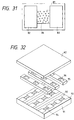
- FIG. 30 A typical construction of the surface conduction type electron-emitting device is shown in Fig. 30.
- This device comprises electrodes 82, 83 for an electric connection, a thin film 85 formed of an electron-emitting material, a substrate (insulating base) 81, and an electron-emitting portion 84.
- the electron-emitting portion is formed by an electric current-heating treatment called "forming".
- forming an electric current-heating treatment
- an electric voltage is applied between the electrode 82 and the electrode 83 to cause a flow of electric current through the thin film 85 and to destroy, deform, or denature locally the thin film 85 by utilizing Joule heat generated.
- the electron-emitting portion 84 having high electric resistance is formed, and thus the function of electron emission is obtained.
- the state of the high electric resistance results from a discontinuity of the thin film 85 in which cracks of 0.5 to 5 ⁇ m in length are formed locally and the cracks have an island structure therein.
- the island structure means a state of the film in which the film contains fine particles of several tens of angstroms to several microns in diameter and the particles are discontinuous but the film is electrically continuous.
- voltage is applied to the aforementioned discontinuous high-resistance film through the electrodes 82, 83 to cause a current flow at the surface of the device, thereby electron being emitted from the fine particles.
- a novel surface conduction type electron-emitting device in which electron-emitting fine particles are distributed between electrodes was disclosed by the inventors of the present invention in Japanese Patent Application Laid-Open Nos. Hei-1-200532 and Hei-2-56822.
- This electron-emitting device has advantages that (1) high electron-emitting efficiency can be obtained, (2) the device can be readily prepared because of its simple construction, (3) many devices can be arranged on one and the same substrate, and so forth.
- Fig. 31 shows a typical construction of such a surface conduction type electron-emitting device, which comprises electrodes 82, 83 for electric connection, an electron-emitting portion 86 having electron-emitting fine particles dispersed therein, and a substrate 81.
- Fig. 32 illustrates an image-forming apparatus having a number of the aforementioned electron-emitting devices arranged therein.
- the apparatus comprises wiring electrodes 92, 93, electron-emitting portions 94, grid electrodes 95, electron-passing holes 96, and an image-forming member 97.
- This image-forming member is made of a material such as fluorescent materials and resist materials which cause light-emission, color change, electrification, denaturing or like changes on collision of electrons.
- the linear electron sources have a plurality of electron-emitting portions 94 arranged between the electrodes 92, 93, and grid electrodes 95 are driven in XY matrix, and electrons are made to collide against the image-forming member 97 in correspondence with information signals to form an image.
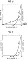
- the electric characteristics (current-voltage characteristics) of conventional surface conduction type of electron-emitting devices are explained by reference to Fig. 6.
- electron emission increases rapidly from a certain device voltage Ve (voltage applied to the device) with increase of the device voltage, and at a device voltage Vd, sufficient electron beam comes to be emitted: for example, a sufficient electron beam for forming an image in the above-mentioned image-forming apparatus.
- the device current If (current which flows in the device) increases with the device voltage, and the rate of the increase becomes larger at around the device voltage Ve.
- a strong ineffective current which is useless for electron emission, as shown in Fig. 6.
- the ratio of the ineffective current to the device current If rises in some cases to as much as about 50 %. Such increase of the ineffective current will cause increase of power consumption in driving the electron-emitting device, and increase of heat generation in the electron-emitting device to deteriorate electron-emitting characteristics (electron-emission efficiency, electron-emission stability, etc.).
- the increase of the ineffective current gives rise to the problems, when the electron-emitting device in which the ineffective current is remarkable is used for an image-forming apparatus: 1) the ineffective current flows to wiring electrodes to cause a voltage drop, whereby the quantity of electron emission varies with the electron-emitting devices, and 2) the ineffective current varies depending on the kind of the image (namely, difference in inputted information signal) to cause a voltage drop in wiring electrode, whereby the quantity of the emitted electrons varies.
- Such disadvantageous phenomena further cause lowering of contrast and sharpness of the formed image; and in particular, in the case where the formed image is a fluorescent image, bring about variation and change of luminance of the fluorescent images, which makes it difficult to obtain fineness of the image and to enlarge a picture screen, and further increase the power consumption.
- Another object of the present invention is to provide an electron-emitting device and an electron beam-generating apparatus which are excellent in electron emission characteristics such as electron-emission efficiency, and electron-emission stability, and which consumes less electric power.
- a further object of the present invention is to provide an electron beam-generating apparatus in which an ineffective current is extremely weak in the whole apparatus, and which gives an image with high contrast and high sharpness with less power consumption, in particular an electron beam-generating apparatus capable of forming a luminescent image with extremely low variation and low fluctuation of luminance.
- an electron emitting device according to claim 1, 24 or 47, respectively.
- Fig. 1 is a plan view illustrating schematically an electron-emitting device of the present invention.
- Fig. 2 is a sectional view of the electron-emitting device at A-A' in Fig. 1.
- Fig. 3 is a sectional view of the electron-emitting device at B-B' in Fig. 2.
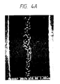
- Fig. 4A is an SEM photograph of an electron-emitting region between electrodes of an electron-emitting device of the present invention (magnification: ⁇ 30,000).
- Fig. 4B is a sketch of an SEM photograph of an electron-emitting region of Fig. 4A (plan view).
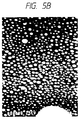
- Fig. 5A is an enlarged SEM photograph of an electron-emitting region of the electron-emitting device of Fig. 4 (magnification: ⁇ 150,000).
- Fig. 5B is an enlarged SEM photograph of an electron-emitting region of the electron-emitting device of Fig. 4 (magnification: ⁇ 800,000).
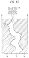
- Fig. 5C is a sketch of the enlarged SEM photograph of an electron-emitting region of Fig. 5A (plan view).
- Fig. 6 shows a current-voltage relation of a conventional electron-emitting device.
- Fig. 7 shows a current-voltage relation of an electron-emitting device of the present invention.
- Fig. 8A is an SEM photograph (magnification: ⁇ 150,000) to explain the method for measuring the voltage application length of the electron-emitting device of the present invention.
- Fig. 8B is a sketch of the SEM photograph of Fig. 8A.
- Fig. 9A is another SEM photograph (magnification: ⁇ 150,000) to explain the method for measuring the voltage application length of the electron-emitting device of the present invention.
- Fig. 9B is a sketch of the SEM photograph of Fig. 9A.
- Fig. 10 is a drawing to explain the method for measuring the voltage application length of the electron-emitting device of the present invention.
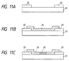
- Figs. 11A to 11C are drawings to explain a method for preparing the electron-emitting device of the present invention (sectional view).
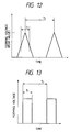
- Fig. 12 shows a wave form of the pulse voltage on forming treatment of an electron-emitting device of the present invention.
- Fig. 13 shows another wave form of the pulse voltage on forming treatment of an electron-emitting device of the present invention.
- Figs 14A to 14E are drawings to explain a method for preparing the electron-emitting device of the present invention (sectional view).
- Figs. 15A to 15D are drawings to explain a method for preparing the electron-emitting device of the present invention (sectional view).
- Fig. 16 illustrates schematically the construction of the measurement apparatus of electron emission characteristics of an electron-emitting device.
- Fig. 17 is a perspective view illustrating schematically an electron beam-generating apparatus of the present invention.
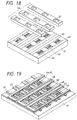
- Fig. 18 is a perspective view illustrating schematically another electron beam-generating apparatus of the present invention.
- Fig. 19 is a perspective view illustrating schematically still another electron beam-generating apparatus of the present invention.
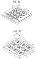
- Fig. 20 is a perspective view illustrating schematically still another electron beam-generating apparatus of the present invention.
- Fig. 21 is a perspective view illustrating schematically still another electron beam-generating apparatus of the present invention.
- Fig. 22 is a perspective view illustrating schematically an image-forming apparatus of the present invention.
- Fig. 23 is a perspective view illustrating schematically another image-forming apparatus of the present invention.
- Fig. 24 is a perspective view illustrating schematically still another image-forming apparatus of the present invention.
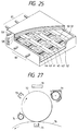
- Fig. 25 is a perspective view illustrating schematically still another image-forming apparatus of the present invention.
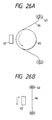
- Figs. 26A and 26B illustrate schematically an image-forming apparatus (optical printer) of the present invention.
- Fig. 27 illustrates schematically another image-forming apparatus (optical printer) of the present invention.
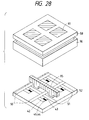
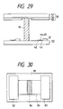
- Fig. 28 illustrates schematically an image forming apparatus provided with a supporting member of the present invention (assembling drawing).
- Fig. 29 is a sectional view of the apparatus of Fig. 28.
- Fig. 30 is a plan view illustrating schematically construction of a conventional electron-emitting device.
- Fig. 31 is a plan view illustrating schematically construction of another conventional electron-emitting device.
- Fig. 32 is a perspective view of a conventional image-forming apparatus.
- Fig. 1 plan view
- Fig. 2 sectional view at A-A' in Fig. 1
- Fig. 3 sectional view at B-B' in Fig. 2).
- the numeral 1 denotes an insulating substrate; 2 and 3, each an electrode; 5, an electron-emitting region; 4, a fine particle film having an electric resistance lower than that of the electron-emitting region 5; and 6, a fine particle dispersed in the electron-emitting region 5.
- the electron-emitting device of the present invention is required essentially to have an electron-emitting region 5 having fine particles 6 dispersed therein, and electrodes 2 and 3 to apply voltage to the interior of the region 5.
- the electron-emitting device of the present invention serves in such a mechanism that electrons pass (or current flows) through the electron-emitting region by application of voltage between the electrodes 2 and 3, and the electrons are emitted out from the gap formed by the fine particles 6 (or spacing between the fine particles) in the region.
- the fine particle film 4 having lower resistance is not an essential requirement in the present invention, but is preferred to improve further the electrical contact between the electron-emitting region 5 and the electrodes 2 and 3.
- the electron-emitting region and the fine particles constituting the fine particle film 4 are both made of an electroconductive material.
- the electron-emitting device of the present invention has to satisfy further another requirement shown below, and is classified into two types of embodiments according to the requirement. It is described in detail.
- the areal occupation ratio of the fine particles is in the range of 20 to 75 % in the electron-emitting region 5.
- Fig. 4A, Fig. 5A, and Fig. 5B are SEM (scanning electron microscope) photographs of an electron-emitting region of an electron-emitting device of the present invention prepared as examples described later.
- Fig. 4B and Fig. 5C are sketches of the SEM photographs.
- Fig. 4A and Fig. 4B shows a view of the region A-A' of Fig. 2 observed from the top.
- Fig. 5A and Fig. 5C shows a view of the region A-A' of Fig. 2 observed from the top.
- the areal occupation ratio in the present invention means the value measured as follows. As shown by the dotted-line area in Fig. 5C, the SEM image of the inside of the electron-emitting region 15 of the element is taken at a magnification such that 10 to 1000 fine particles are observed (Fig. 5B).
- the relations of the areal occupation ratio of the fine particles with the aforementioned ineffective current flowing in the device, and with the electron-emitting characteristics of the device are considered as below by the inventors of the present invention. If the areal occupation ratio of the fine particles is excessively large, the ratio of the aforementioned gap to the entire electron-emitting region is extremely small, and the the electron-emitting region behaves as a continuous film. Therefore, the quantity of electrons flowing through the continuous film is larger than the quantity of electrons emitted from the gap. As the results, the the ineffective current becomes stronger, and quantity of the emitted electrons decreases.
- the areal occupation ratio of the fine particles is in the range of from 20 to 75 %, more preferably from 35 to 60 %, the ineffective current of the electron-emitting device is effectively made extremely small, and the quantity of electron emission is increased, and further thereby the electron-emission efficiency and the electron-emission stability are improved effectively. Consequently, the present invention has been completed.
- the average particle diameter of the fine particles dispersed in the electron-emitting region is adjusted preferably to be in the range of from 5 to 300 ⁇ , more preferably 5 to 80 ⁇ . With the average diameter within this range, the ineffective current flowing through very large particles can be suppressed, the ineffective current in the whole device can further be reduced, and the electron emission efficiency and the electron emission stability (in particular, flickering of electron emission) are improved more.
- the gap between the fine particles 6 in the electron-emitting region 5 is in the range of from 5 to 100 ⁇ , and the average particle diameter of the fine particles is in the range of from 5 to 1000 ⁇ .
- the gap between the fine particles in the present invention means the spacing of particles as shown by the symbol S in Fig. 3.
- the gap S of the fine particles and the average particle diameter t are measured as follows. As shown by the dotted-line area in Fig. 5, the SEM image of the inside of the electron-emitting region 15 (photograph) of the element is taken at a magnification such that 10 to 1000 fine particles are observed.
- the dependence of the ineffective current flowing in the device and the electron emission characteristics of the device on the fine particle gap and the average diameter are considered as below by the inventors of the present invention. If the average particle diameter is excessively large and the fine particle gap is extremely small, the ratio of the aforementioned gap to the entire electron-emitting region is too small, and the electron-emitting region behaves as a continuous film. Therefore, the quantity of electrons flowing through the continuous film is larger than the quantity of electrons emitted from the gap. As the results, the ineffective current becomes large, and quantity of the emitted electrons decreases.
- the gap of the fine particles is adjusted to be within the range of from 5 to 100 ⁇ , preferably 5 to 50 ⁇ , the ineffective current of the electron-emitting device is effectively made extremely small, and the quantity of electron emission is increased, and further thereby the electron emission efficiency and the electron emission stability are improved effectively. Consequently, the present invention has been completed.
- the average particle diameter of the fine particles dispersed in the electron-emitting region is adjusted preferably to be in the range of from 5 to 300 ⁇ , more preferably 5 to 80 ⁇ due to the same reason as in the above-described first embodiment.
- the electron-emitting device which meets simultaneously the both requirements of the two types of embodiments is more preferable in the present invention. That is, if the areal occupation ratio in the electron-emitting region is from 20 to 75 %, the gap of the particles is from 5 to 100 ⁇ , and the average particle diameter of the fine particles is from 5 to 1000 ⁇ , then the electron-emitting device is improved in comparison with each of the above embodiments in reducing the ineffective current in the device and is superior in electron emission quantity, electron emission efficiency, and electron emission stability (prevention of flickering of electron emission), and further the device is driven with lower voltage and has longer life.
- the above effects are more remarkable if the areal occupation ratio is from 35 to 60 %, and the particle gap is from 5 to 50 ⁇ .
- the effects are still more remarkable if the average particle diameter is from 5 to 300 ⁇ , more preferably 5 to 80 ⁇ .
- the methods for controlling the areal occupation ratio, the fine particle gap, and the fine particle diameter are described below.
- the control of these parameters were practiced as follows.
- the gap between the electrodes was set in the range of 0.2 to 5 ⁇ m.
- An electroconductive film having a sheet resistance of 3 ⁇ 10 3 ⁇ /cm 2 to 10 7 ⁇ /cm 2 was formed by placing electroconductive particles of 5 to 100 ⁇ in particle diameter in dispersion between the electrodes.
- a specified wave form of voltage pulse was applied to the electrodes.
- the applied voltage pulse is suitably decided depending on the shape of the electrodes, the material of the electroconductive film, and the material of the substrate.
- the material of the electroconductive particles includes metals such as Pd, Nb, Mo, Rh, Hf, Ta, W, Re, Ir, Pt, Ti, Au, Ag, Cu, Cr, Al, Co, Ni, Fe, Pb, Cs, and Ba; borides such as LaB 6 , CeB 6 , HfB 4 , and GdB 4 ; carbides such as TiC, ZrC, HfC, TaC, SiC, and WC; nitrides such as TiN, ZrN, and HfN; metal oxides such as PdO, Ir 2 O 3 , SnO 2 , and Sb 2 O; semiconductors such as Si, and Ge; carbon, Ag, Mg, and the like.
- the above method is preferred in controlling the parameters.
- the large ineffective current of the conventional electron-emitting device as described above was further studied by the inventors of the present invention. As the results, it was found that the strength of the ineffective current flowing through the electron-emitting device varies depending on the size of the region where the voltage for driving the device is effectively applied (the size being referred to as "voltage application length"). It was further found that the ineffective current can be suppressed to extremely small by adjusting the voltage application length within a certain range, the ineffective current of the device being negligible at the voltage application length of from 5 to 300 ⁇ , preferably 5 to 50 ⁇ .
- the voltage application length in more detail, means a length of the region where the voltage is effectively applied as described above in the electron-emitting device. In this region, voltage drops substantially, but outside the region, the voltage does not drop substantially.
- Fig. 8A is an SEM photograph of an area between the electrodes on application of voltage to an electron-emitting device of the present invention.
- Fig. 8B is a sketch of the SEM photograph of Fig. 8A.
- Fig. 9A is an SEM photograph of an area between the electrodes of the same electron-emitting device on application of voltage in the reversed direction.
- Fig. 9B is a sketch of the SEM photograph of Fig. 9A. In Fig 8B and Fig.
- the numeral 15 denotes an electron-emitting region
- the numeral 14 denotes an electroconductive film for sufficient electric contact of electrodes (not shown in the drawing) with the electron-emitting region
- the numeral 17 denotes a portion from which the secondary electron emission is less. This portion is observed to be dark in the actual SEM image (Fig. 8A and Fig. 9B).
- the SEM photograph of the area between the device electrodes to be measured is taken by applying to the electrodes a voltage of 1.5 V to 4.0 V under a vacuum of 1 ⁇ 10 3 to 1 ⁇ 10 -6 torr. Then, the same SEM photograph is taken by applying the same voltage in the reversed direction at the same magnification.
- the obtained two SEM images are superposed as shown in Fig. 10.
- the maximum width L of the blank area 18 in the electron-emitting region 15 is measured, from which the real length is calculated in consideration of the magnification of the SEM.
- STM may be employed for measurement.
- a voltage of 1 to 2.5 V is applied to the device, and the probe of the STM is driven to scan the area to be measured from the negative potential side to the positive potential electrode side.
- the length of the region where 30 % to 70 % of the applied voltage is observed is taken as the voltage application length.
- the control of the voltage application length and the electric field strength of the electron-emitting device was practiced as below.
- the gap between the electrodes was set in the range of from 0.2 to 5 ⁇ m.
- An electroconductive film having a sheet resistance of from 3 ⁇ 10 3 ⁇ /square to 10 7 ⁇ /square was formed.
- a specified wave form of voltage pulse was applied through the electrodes.
- the applied voltage pulse is suitably decided depending on the shape of the electrodes, the material of the electroconductive film, and the material of the substrate.
- the electroconductive film is preferably formed, as described later in Examples, by placing electroconductive particles of from 5 to 1000 ⁇ in particle diameter in dispersion between the electrodes, the material thereof is those mentioned above.
- the electron-emitting devices of the above embodiments exhibit extremely small ineffective current, the ineffective current being 2% or less, in more preferred embodiment, 1 % or less.
- the electron-emitting device of any embodiment of the present invention is excellent in electron-emitting characteristics such as electron emission quantity, electron emission efficiency, and emission stability (prevention of flickering of electron emission).
- the electron beam-generating apparatus and the image-forming apparatus of the present invention are described below in detail.
- the electron beam-generating apparatus and the image-forming apparatus of the present invention are characterized by the use of the above-described electron-emitting devices.
- the electron beam-generating apparatus of the present invention comprises a plurality of the above electron-emitting devices, and modulation means for modulating electron beams emitted from the electron-emitting devices in accordance with information signals.
- the numeral 41 denotes an insulating substrate; 42 and 43, electrodes; 45, an electron-emitting region; 44, an electroconductive film for obtaining sufficient electric contact between the electrode and the electron-emitting region; and 46, a modulation means.
- linear electron-emitting devices having a plurality of electron-emitting regions are juxtaposed on the substrate, and a plurality of grid electrodes (modulation electrodes) 46 are placed in an XY matrix with the linear electron-emitting devices.
- the grid electrodes are placed above the electron-emitting face of the electron-emitting device in Fig. 18; juxtaposed on the same substrate plane as the electron-emitting devices in Fig.
- a plurality of electron-emitting devices having each a single electron-emitting portion are arranged in matrix, and each element is connected to a signal wiring electrode 50 and a scanning wiring electrode 51 as shown in the drawing.
- This construction is called a simple matrix construction, in which the signal wiring electrodes 50 and the scanning wiring electrodes 51 serves as the modulation means.
- the electron beam-generating apparatuses exemplified above are driven as below. To drive the apparatus illustrated in Fig.
- a pulsing voltage of 10 to 35 V is applied to the electrodes 42 and 43 of one line of the linear electron-emitting devices to cause emission of electron beams from a plurality of the electron-emitting portions.
- the emitted electron beams are turned on and off by the application of a voltage of 50 V to -70 V to the grid electrodes 46 in correspondence with information signals to obtain electron emission corresponding to the information signals for the one line.
- Such operation is conducted sequentially for the adjacent lines of the linear electron-emitting devices to obtain electron beam emission for one picture image.
- a pulsing voltage is applied with the scanning wiring electrode 51 to the plurality of the electron-emitting devices on one line, and subsequently a pulsing voltage is applied to the signal wiring electrodes 50 in correspondence with information signals to obtain electron emission corresponding to information signal for one line. Such operation is conducted sequentially for adjacent lines to obtain electron beam emission for one picture image.
- the electron beam-generating apparatus of the present invention is advantageous in that the ineffective current in the whole apparatus is extremely week, electron-emitting characteristics such as electron emission efficiency and electron emission stability are excellent, and power consumption is low.
- the image-forming apparatus of the present invention has a constitution such that an image-forming member is placed on the electron beam emission side of the aforementioned electron beam-generating apparatus.
- the image-forming member is constituted of a material which causes light emission, color change, electrification, denaturing, etc. on collision of electrons, such as a light-emitting material like a fluorescent material, and a resist material.
- Fig. 22 illustrates one embodiment of an image-forming apparatus of the present invention.
- the apparatus of Fig. 22 comprises a rear plate 52 (which may serve also as the aforementioned insulating substrate 41), modulation means 46 (which are shown in a form of grid electrodes of Fig. 18, but may be the grid electrodes of Fig.
- Electrodes 42 and 43 for obtaining sufficient electric contact between the electrodes and the electron-emitting regions, a face plate 58, a glass plate 57, a transparent electrode 55, and a fluorescent material 56.
- a voltage of 0.5 KV to 10 KV is applied to the image-forming member (transparent electrode 55 in Fig. 22), and then the apparatus is driven in the same manner as driving of the above-described electron beam-generating apparatus, and thus an image corresponding to information signals is obtained on the image-forming member (fluorescent image in Fig. 22).
- the image-forming member is made of a light-emitting material such as a fluorescent material
- a full-color image display can be obtained by using three light-emitting materials of three primary colors of red, green, and blue for one picture element.
- the electron beam-generating apparatus and the image-forming apparatus described above are usually driven at a vacuum of 10 -4 to 10 -9 torr.
- the image-forming apparatus of the present invention includes the embodiment shown in Fig. 28 and Fig. 29.
- a supporting member for supporting the atmospheric pressure is provided between the face plate 58 and the rear plate 52 in the image-forming apparatus of Fig. 23, Fig. 24, or Fig. 25.
- Fig. 28 illustrates schematically the construction of an image-forming member of the present invention.
- Fig. 29 is a sectional view of the image-forming apparatus viewed at around the atmospheric pressure-supporting member of the image-forming apparatus shown in Fig 28.
- the numeral 95 denotes an atmospheric pressure-supporting member; 96, a supporting frame; and 97, a luminescent spot of the fluorescent substance.
- An envelop of the image-forming apparatus is constructed of a face plate 58, a rear plate 52, and a supporting frame 96.
- the internal pressure is kept at a vacuum of 10 -4 to 10 -9 torr.
- an atmospheric pressure-supporting member is provided desirably.
- the atmospheric pressure-supporting members 95 are placed usually at intervals of 1 mm to 100 mm between the picture elements so that image defect may be avoided.
- the material of the atmospheric pressure-supporting member 95 is an insulating material such as glass.
- the supporting member When the image-forming apparatus having an atmospheric supporting member 95 as shown in Fig. 28 and Fig. 29 is driven, the supporting member is liable to be electrically charged by unexpected collision of electron beam or ions against the supporting member 95 since the supporting member 95 is electrically floating.
- This electric charging bends the locus of the electron beam and changes the amount of the electron beam colliding to the fluorescent material, causing irregularity of luminance and color.
- the disadvantage caused by the electric charging of the supporting member relates to driving voltage of the electron-emitting device. If the ineffective current of the electron-emitting device is large, the voltage applied to the device is high, and the supporting member 95 becomes liable to be charged. Accordingly, in the present invention, use of an electron-emitting device causing weak ineffective current makes it possible to obtain an image-forming apparatus with a large picture area and light weight.
- the image-forming apparatus of the present invention includes the embodiments shown in Fig. 26 and Fig. 27, which are examples of optical printers employing as the light source of the image-forming apparatus illustrated in Fig. 22.
- the numeral 62 denotes the light source; 65 a drum; 63, a delivery roller; and 64, a heat-sensitive or light-sensitive sheet.
- the optical printer records an image on a recording medium by driving the light source as described above (as driving of the image-forming apparatus of Fig. 22) to emit light in correspondence with information signals onto the recording medium 64 with scanning of the recording medium 64 supported by a support 65 or 63, or the light source 62.
- Fig. 27 illustrates another embodiment of the optical printer.
- the numeral 71 denotes a light source; 72, a drum-shaped recording medium; 77, a developer; 75, a static eliminator; 74, a cleaner; 73, an electric charger; and 76, an image-transfer medium.
- This optical printer records an image by electrically charging the recording medium 72 with an electric charger 73, projecting a light beam emitted from the light source 71 in a manner as above (driving method of the image-forming apparatus of Fig. 22) to the recording medium 72 to eliminate electric charge from the illuminated area, adhering a toner on the non-illuminated area by means of a developer 77, and transferring the toner onto the image-transfer medium 76 by eliminating the electric charge at the position of the static eliminator 75.
- the image-forming apparatus of the present invention as described above is capable of forming an image with high contrast and sharpness with less consumption of electric power.
- the image-forming apparatus utilizing luminescent image gives extremely small variation or flickering of the luminance.
- Electron-emitting devices of the type'shown in Figs. 1 to 3 were prepared. The procedure of the preparation is described below by reference to Fig. 11.
- the pulse width T 1 was 1.0 millisecond, and the pulse interval T 2 was 10 milliseconds in this Example.
- the forming treatment was conducted at the forming voltage as shown below. under a vacuum environment of about 1 ⁇ 10 -6 torr.
- the electron-emitting region 25 was formed between the fine palladium oxide film 4, and was composed of fine palladium particles 6 as shown in Fig. 3.
- the fine particles 6 had an average diameter of 10 ⁇ .
- Three devices of different areal occupation ratio of the fine particles 6 were prepared by changing the amount of the coating of the organic palladium to change a sheet resistance of the fine particle film 24 in the step (2) and changing the forming voltage in the step (3).
- Fig. 16 illustrates schematically the construction of the measuring apparatus.
- the measuring apparatus comprises an insulating substrate 21, electrodes 22 and 23, an electron-emitting region 25, electroconductive films 24 for obtaining electric contact, a power source 31 for applying voltage to the device, an ammeter 30 for measuring the device current (If), an anode electrode 34 for measuring emission current (Ie) emitted from the device, a high-voltage power source 33 for applying a voltage to the anode electrode 34, and an ammeter 32 for measuring the emission current.
- the aforementioned device current means the current measured by the ammeter 30, and the emission current means the current measured by the ammeter 32.
- Electron-emitting devices were prepared by the procedure below.
- Two kinds of devices were prepared by changing the voltage in the forming treatment.
- An electron-emitting device was prepared in the same manner as in Example 2 except that the sheet resistance of the fine particle film 24 was 5 ⁇ 10 5 ⁇ /square and the forming voltage was 4 V. In the resulting device, the areal occupation ratio of the fine particles 6 was 50 %, and the average particle diameter of the fine particles 6 was 5 ⁇ . The electron-emitting device exhibited approximately the same effect as the ones in Example 2 (ineffective current being not more than 1 %).
- Electron-emitting devices were prepared as below.
- Three kinds of devices were prepared by changing the amount of the coating of the organic palladium to change the sheet resistance of the fine particle film 24 and by changing the forming voltage as below:
- An electron-emitting device was prepared in the same manner as in Example 4 except that the sheet resistance of the fine particle film 24 was 1 ⁇ 10 5 ⁇ /square and the forming voltage was 4 V. In the resulting device, the average particle gap was 5 ⁇ , and the average particle diameter was 50 ⁇ . The electron-emitting device exhibited approximately the same effect as the ones in Example 4 (ineffective current being not more than 3 %).
- An electron-emitting device was prepared in the same manner as in Example 4 except that the sheet resistance of the fine particle film 24 was 5 ⁇ 10 3 ⁇ /square and the forming voltage was 14 V. In the resulting device, the average particle gap was 100 ⁇ , and the average particle diameter was 50 ⁇ . The electron-emitting device exhibited approximately the same effect as the ones in Example 4 (ineffective current being not more than 1 %).
- Electron-emitting devices were prepared as below.
- Two kinds of devices were prepared by changing the amount of coating to change the sheet resistance of the fine particle film 24, and by changing the forming voltage.
- An electron-emitting device was prepared in the same manner as in Example 7 except that the sheet resistance of the fine particle film 24 was 3 ⁇ 10 5 ⁇ /square and the forming voltage was 4 V. In the resulting device, the average particle gap was 30 ⁇ , and the average particle diameter was 5 ⁇ . The electron-emitting device exhibited approximately the same effect as the ones in Example 7 (ineffective current being not more than 1.0 %).
- Electron-emitting devices were prepared as below. The procedures explained by reference to Fig. 14.
- Figs. 14A to 14C were practiced in the same manner as in the steps (1) to (3) in Example 1 except that the forming treatment was conducted with the voltage wave form as shown in Fig. 12 at the forming voltage of 8 V, the pulse width of T 1 of 1 millisecond, and the pulse interval T 2 of 10 milliseconds.
- An electron-emitting device was prepared in the same manner as in Example 9 except that the steps (4) and (5) were conducted four times.
- the areal occupation ratio of the fine particles in the electron-emitting region was 75 %
- the average particle diameter of the fine particles was 35 ⁇
- the average gap of the fine particles was 5 ⁇ .
- the device was evaluated in the same manner as in Example 9. The effect was nearly the same as that of Example 9 (ineffective current: not more than 2.0 %).
- An electron-emitting device was prepared in the same manner as in Example 9 except that in the step (4) the forming voltage was 12 V.
- the areal occupation ratio of the fine particles in the electron-emitting region was 20 %
- the average particle diameter of the fine particles was 25 ⁇
- the average gap of the fine particles was 100 ⁇ .
- the device was evaluated in the same manner as in Example 9. The effect was nearly the same as that of Example 9 (ineffective current: not more than 0.2 %).
- An electron-emitting device was prepared in the same manner as in Example 9 except that in the step (4) the forming voltage was 12 V, and the steps (4) and (5) were conducted twice.
- the areal occupation ratio of the fine particles in the electron-emitting region was 50 %
- the average particle diameter of the fine particles was 300 ⁇
- the average gap of the fine particles was 30 ⁇ .
- Example 9 The device was evaluated in the same manner as in Example 9. The effect was nearly the same as that of Example 9 (ineffective current: not more than 1.0 %).
- Electron-emitting devices were prepared as below. The procedures explained by reference to Fig. 15.
- An electron ray-generating apparatus was prepared by arranging in a line a plurality of the electron-emitting devices prepared in Examples 1 - 13 as shown in Fig. 17.
- the apparatus comprises an insulating substrate (a rear plate) 41, wiring electrodes 42 and 43, low-resistance portions 44 having low electric resistance, electron-emitting regions 45, modulation means (grid electrodes) G 1 to G L (46), and electron-passing holes 47.
- the spacing between the insulating substrate 41 and the modulation means 46 was adjusted to 10 ⁇ m.
- the electron beam-generating apparatus was driven as described below.
- the apparatus was placed in the vacuum of 10 -6 torr.
- a driving voltage (device voltage in Examples 1 - 13) was applied between the wiring electrodes.
- a voltage of 30 V was applied to the modulation means in accordance with information signals. Thereby, electron beams were emitted from the plurality of the regions 45 in accordance with the information signals.
- the electron beam-generating apparatus of this Example consumed less electric power because the ineffective current in the device current was extremely low (2 % or less). Therefore, the electron-emitting devices could be arranged in fine pitch in the apparatus. Further, since the current flowing through the electrodes 42 and 43 was weak, the voltage drop between the electrodes 42 and 43 was small, and the quantities of the electron beams (or emission current) emitted from the elements were uniform. Therefore, many elements could be arranged between the electrodes 42 and 43.
- An electron beam-generating apparatus was prepared by arranging in lines a plurality of linear electron-emitting device groups comprising the electron-emitting devices of Examples 1 - 13, as shown in Fig. 18.
- the spacing between the insulating substrate 41 and the modulation means 46 was adjusted to 10 ⁇ m, and the interval between the linear electron-emitting device groups was adjusted to 1 mm.
- the electron beam-generating apparatus was driven as described below.
- the apparatus was placed in the vacuum of 10 -6 torr.
- the driving voltage (device voltage in Examples 1 - 13) was applied between the wiring electrodes 42 and 43.
- a voltage was applied to the modulation means 46 in accordance with information signals: the electron beam being controlled to be off at 0 V or lower, being controlled to be on at +30 V or higher, and to vary continuously between 30 V and 0 V. Consequently, electron beams were emitted from a plurality of electron-emitting region 45 in a line between the wiring electrodes 42 and 43 in accordance with the one line of information. This operation was conducted sequentially for adjacent lines of the linear electron-emitting device group to obtain electron emission for the entire information signals.
- Example 14 In this Example also, the similar effects as in Example 14 were confirmed.
- An electron beam-generating apparatus was prepared in the same manner as in Example 15 except that the modulation means (grid electrodes) 46 were placed on the face of the insulating substrate 41.
- the emission of electron beams could be made in accordance with information signals by driving the apparatus in a similar manner as in Example 15.
- the electron beams could be controlled by the voltage applied to the modulation means: to be off at -30 V or lower, to be on at +20 V or higher, and to vary continuously between -30 V and +20 V.
- Example 14 In this Example also, the similar effects as in Example 14 were confirmed.
- An electron beam-generating apparatus was prepared in the same manner as in Example 15 except that the modulation means (grid electrodes) 46 were placed on the face of the insulating substrate opposite to the electron-emitting face of the linear electron-emitting device groups.
- the emission of electron could be made in accordance with information signals by driving the apparatus in a similar manner as in Example 15.
- the electron beams could be controlled by the voltage applied to the modulation means: to be off at -30 V or lower, to be on at +20 V or higher, and to vary continuously between -30 V and +20 V.
- Example 14 In this Example also, the similar effects as in Example 14 were confirmed.
- the electron beam-generating apparatus of this Example has the construction shown schematically in Fig. 21.
- this apparatus having a simple matrix construction, a plurality of electron-emitting devices of any of Examples 1 to 13 are arranged in matrix, and each device is connected to a signal wiring electrode 50 and a scanning wiring electrode 51.
- the apparatus was driven as described below.
- the device voltage indicated in Examples 1 to 13 was applied to each of the electron-emitting devices to cause electron emission from the electron-emitting devices. Firstly, pulsing voltage of 0 V or half the device voltage was applied by the scanning wiring electrode 51 to one line of a plurality of the electron-emitting devices. Then another pulsing voltage of 0 V or half the device voltage was applied to the signal wiring electrode 50 in correspondence with information signals to obtain the electron beam emission in correspondence with the information signals for the one line. Such operation was conducted sequentially for adjacent lines to obtain electron beam emission for one picture image.
- Example 14 In this Example also, the similar effects as in Example 14 were confirmed.
- FIG. 22 An image-forming apparatus as shown in Fig. 22 was prepared by use of the electron beam-generating apparatus of Example 15.
- the numeral 58 denotes a face plate; 57, a glass plate; 55, a transparent electrode; and 56, a fluorescent material.
- the spacing between the face plate 58 and the rear plate 52 was adjusted to be 3 mm.
- the image-forming apparatus was driven in a manner shown below.
- the panel vessel constructed from the face plate 58 and the rear plate 52 was evacuated to a vacuum of 10 -6 torr; the voltage of the fluorescent material face was set through the EV terminal 59 at 5 KV to 10 KV; and pulsing voltage (namely the device voltage indicated in Example 1 to 13) was applied to a pair of wiring electrodes 42 and 43.
- the electron beams were emitted through the modulation means in accordance with the information signals collided against the fluorescent material 56 to display one line of information of the information signal. This operation was sequentially conducted to obtain a display of entire picture.
- the image displayed by the image-forming apparatus of this Example exhibited low irregularity in luminance, and gave a sharp image with high contrast.
- the image-forming apparatus having a well-known constitution of a cathode beam tube gave a sharp color image with high contrast with less irregularity of luminance by use of a face plate employing color fluorescent materials of R (red), G (green), and B (blue).
- An image-forming apparatus as shown in Fig. 23 was prepared by use of the electron beam-generating apparatus of Example 16.
- the apparatus was driven to display a luminescent image of the fluorescent material in the same manner as in Example 19, except that the voltage applied to the modulation means was - 40 V or lower to control the electron beam to be off and +10 V or higher to control the electron beam to be on.
- the voltage applied to the modulation means was - 40 V or lower to control the electron beam to be off and +10 V or higher to control the electron beam to be on.
- the voltage applied to the modulation means was - 40 V or lower to control the electron beam to be off and +10 V or higher to control the electron beam to be on.
- the voltage range between -40 V to +10 V the quantity of the electron of the electron beam varies continuously, thereby gradation of display being practicable.
- Example 19 also, the same effects as in Example 19 were confirmed.
- An image-forming apparatus as shown in Fig. 24 was prepared by use of the electron beam-generating apparatus of Example 17.
- the apparatus was driven to display a luminescent image of the fluorescent material in the same manner as in Example 19, except that the voltage applied to the modulation means was -40 V or lower to control the electron beam to be off and +10 V or higher to control the electron beam to be on.
- the voltage applied to the modulation means was -40 V or lower to control the electron beam to be off and +10 V or higher to control the electron beam to be on.
- the voltage applied to the modulation means was -40 V or lower to control the electron beam to be off and +10 V or higher to control the electron beam to be on.
- the voltage applied to the modulation means was -40 V or lower to control the electron beam to be off and +10 V or higher to control the electron beam to be on.
- the quantity of the electron of the electron beam varies continuously, thereby gradation of display being practicable.
- Example 19 also, the same effects as in Example 19 were confirmed.
- FIG. 25 An image-forming apparatus shown in Fig. 25 which is similar to the one of Example 19 was prepared by use of the electron beam-generating apparatus of Example 18.
- the numerals 51 and 52 respectively denote a wiring connected to the scanning wiring electrode and a wiring connected to the signal wiring electrode.
- the image-forming apparatus was driven in a manner shown below.
- the panel vessel constructed from the face plate 58 and the rear plate 52 was evacuated to a vacuum of 10 -6 torr; the voltage of the fluorescent material face was set through the EV terminal 59 at 5 KV to 10 KV.
- Electron beams were emitted from the electron-emitting devices on application of the device voltage indicated in Examples 1 to 13 to the electron-emitting devices. Firstly, pulsing voltage of 0 V or half the device voltage was applied by the scanning wiring electrode 51 to one line of a plurality of the electron-emitting devices.
- Example 14 In this Example also, the similar effects as in Example 14 were confirmed.
- An image-forming apparatus shown in Fig. 28 was prepared by providing an atmospheric pressure-supporting member 95 additionally in the image-forming apparatus of Example 22.
- the apparatus was driven in the same manner as in Example 22, and nearly the same results were obtained, Furthermore, the face plate and the rear plate could be made thinner, whereby the weight of the image-forming apparatus could be reduced, and the picture screen could be enlarged.
Landscapes
- Cathode-Ray Tubes And Fluorescent Screens For Display (AREA)
- Cold Cathode And The Manufacture (AREA)
- Image-Pickup Tubes, Image-Amplification Tubes, And Storage Tubes (AREA)
Abstract
Description
- The present invention relates to a cold-cathode type of an electron-emitting device. The present invention also relates to an electron beam-generating apparatus, and an image-forming apparatus employing the electron-emitting device.
- Cold cathode devices are known as devices capable of emitting electrons with a simple structure. For example, a cold cathode device is reported by M.I. Elinson (Radio Eng. Electron Phys., vol. 10, pp. 1290-1296 (1965)). These devices are based on the phenomenon that electrons are emitted by a flow of an electric current in parallel through a thin film of small area formed on a substrate. Such devices are called generally surface-conduction type electron-emitting devices. The surface-conduction type electron-emitting devices include the ones using a thin SnO2 (Sb) film developed by M.I. Elinson as mentioned above; the ones using a thin Au film (G. Dittmer: "Thin Solid Films", vol. 9, p. 317, (1972)); and the ones using a thin ITO film (M. Hartwell and C.G. Fonstad: IEEE Trans. ED Conf., p. 519 (1975)).
- A typical construction of the surface conduction type electron-emitting device is shown in Fig. 30. This device comprises
electrodes thin film 85 formed of an electron-emitting material, a substrate (insulating base) 81, and an electron-emitting portion 84. Conventionally, in such a surface conduction type electron-emitting device, the electron-emitting portion is formed by an electric current-heating treatment called "forming". In this treatment, an electric voltage is applied between theelectrode 82 and theelectrode 83 to cause a flow of electric current through thethin film 85 and to destroy, deform, or denature locally thethin film 85 by utilizing Joule heat generated. Thereby, the electron-emitting portion 84 having high electric resistance is formed, and thus the function of electron emission is obtained. Here the state of the high electric resistance results from a discontinuity of thethin film 85 in which cracks of 0.5 to 5 µm in length are formed locally and the cracks have an island structure therein. The island structure means a state of the film in which the film contains fine particles of several tens of angstroms to several microns in diameter and the particles are discontinuous but the film is electrically continuous. In a conventional surface conduction type electron-emitting device, voltage is applied to the aforementioned discontinuous high-resistance film through theelectrodes - A novel surface conduction type electron-emitting device in which electron-emitting fine particles are distributed between electrodes was disclosed by the inventors of the present invention in Japanese Patent Application Laid-Open Nos. Hei-1-200532 and Hei-2-56822. This electron-emitting device has advantages that (1) high electron-emitting efficiency can be obtained, (2) the device can be readily prepared because of its simple construction, (3) many devices can be arranged on one and the same substrate, and so forth. Fig. 31 shows a typical construction of such a surface conduction type electron-emitting device, which comprises
electrodes emitting portion 86 having electron-emitting fine particles dispersed therein, and asubstrate 81. - In recent years, attempts were made to use the aforementioned surface conduction type electron-emitting device for an image-forming apparatus. One example is shown in Fig. 32, which illustrates an image-forming apparatus having a number of the aforementioned electron-emitting devices arranged therein. The apparatus comprises
wiring electrodes portions 94,grid electrodes 95, electron-passing holes 96, and an image-formingmember 97. This image-forming member is made of a material such as fluorescent materials and resist materials which cause light-emission, color change, electrification, denaturing or like changes on collision of electrons. With this image-forming apparatus, the linear electron sources have a plurality of electron-emittingportions 94 arranged between theelectrodes grid electrodes 95 are driven in XY matrix, and electrons are made to collide against the image-formingmember 97 in correspondence with information signals to form an image. - The electric characteristics (current-voltage characteristics) of conventional surface conduction type of electron-emitting devices are explained by reference to Fig. 6. In conventional electron-emitting devices, electron emission increases rapidly from a certain device voltage Ve (voltage applied to the device) with increase of the device voltage, and at a device voltage Vd, sufficient electron beam comes to be emitted: for example, a sufficient electron beam for forming an image in the above-mentioned image-forming apparatus. The device current If (current which flows in the device) increases with the device voltage, and the rate of the increase becomes larger at around the device voltage Ve. Generally, in such conventional devices flows a strong ineffective current, which is useless for electron emission, as shown in Fig. 6. The ratio of the ineffective current to the device current If rises in some cases to as much as about 50 %. Such increase of the ineffective current will cause increase of power consumption in driving the electron-emitting device, and increase of heat generation in the electron-emitting device to deteriorate electron-emitting characteristics (electron-emission efficiency, electron-emission stability, etc.). Further, the increase of the ineffective current gives rise to the problems, when the electron-emitting device in which the ineffective current is remarkable is used for an image-forming apparatus: 1) the ineffective current flows to wiring electrodes to cause a voltage drop, whereby the quantity of electron emission varies with the electron-emitting devices, and 2) the ineffective current varies depending on the kind of the image (namely, difference in inputted information signal) to cause a voltage drop in wiring electrode, whereby the quantity of the emitted electrons varies. Such disadvantageous phenomena further cause lowering of contrast and sharpness of the formed image; and in particular, in the case where the formed image is a fluorescent image, bring about variation and change of luminance of the fluorescent images, which makes it difficult to obtain fineness of the image and to enlarge a picture screen, and further increase the power consumption.
- Therefore, it is an object of the present invention to provide an electron-emitting device and an electron beam-generating apparatus in which ineffective current is extremely weak.
- Another object of the present invention is to provide an electron-emitting device and an electron beam-generating apparatus which are excellent in electron emission characteristics such as electron-emission efficiency, and electron-emission stability, and which consumes less electric power.
- A further object of the present invention is to provide an electron beam-generating apparatus in which an ineffective current is extremely weak in the whole apparatus, and which gives an image with high contrast and high sharpness with less power consumption, in particular an electron beam-generating apparatus capable of forming a luminescent image with extremely low variation and low fluctuation of luminance.
- According to the present invention, the above objects are achieved by an electron emitting device according to
claim - Furthermore, according to the present invention, the above objects are achieved by an electron beam-generating apparatus according to
claim - Moreover, according to the present invention, the above objects are achieved by an image forming apparatus according to
claim - Advantageous further developments of the present invention are as set out in the respective dependent claims.
- Fig. 1 is a plan view illustrating schematically an electron-emitting device of the present invention.
- Fig. 2 is a sectional view of the electron-emitting device at A-A' in Fig. 1.
- Fig. 3 is a sectional view of the electron-emitting device at B-B' in Fig. 2.
- Fig. 4A is an SEM photograph of an electron-emitting region between electrodes of an electron-emitting device of the present invention (magnification: ×30,000).
- Fig. 4B is a sketch of an SEM photograph of an electron-emitting region of Fig. 4A (plan view).
- Fig. 5A is an enlarged SEM photograph of an electron-emitting region of the electron-emitting device of Fig. 4 (magnification: ×150,000).
- Fig. 5B is an enlarged SEM photograph of an electron-emitting region of the electron-emitting device of Fig. 4 (magnification: ×800,000).
- Fig. 5C is a sketch of the enlarged SEM photograph of an electron-emitting region of Fig. 5A (plan view).
- Fig. 6 shows a current-voltage relation of a conventional electron-emitting device.
- Fig. 7 shows a current-voltage relation of an electron-emitting device of the present invention.
- Fig. 8A is an SEM photograph (magnification: ×150,000) to explain the method for measuring the voltage application length of the electron-emitting device of the present invention.
- Fig. 8B is a sketch of the SEM photograph of Fig. 8A.
- Fig. 9A is another SEM photograph (magnification: ×150,000) to explain the method for measuring the voltage application length of the electron-emitting device of the present invention.
- Fig. 9B is a sketch of the SEM photograph of Fig. 9A.
- Fig. 10 is a drawing to explain the method for measuring the voltage application length of the electron-emitting device of the present invention.
- Figs. 11A to 11C are drawings to explain a method for preparing the electron-emitting device of the present invention (sectional view).
- Fig. 12 shows a wave form of the pulse voltage on forming treatment of an electron-emitting device of the present invention.
- Fig. 13 shows another wave form of the pulse voltage on forming treatment of an electron-emitting device of the present invention.
- Figs 14A to 14E are drawings to explain a method for preparing the electron-emitting device of the present invention (sectional view).
- Figs. 15A to 15D are drawings to explain a method for preparing the electron-emitting device of the present invention (sectional view).
- Fig. 16 illustrates schematically the construction of the measurement apparatus of electron emission characteristics of an electron-emitting device.
- Fig. 17 is a perspective view illustrating schematically an electron beam-generating apparatus of the present invention.
- Fig. 18 is a perspective view illustrating schematically another electron beam-generating apparatus of the present invention.
- Fig. 19 is a perspective view illustrating schematically still another electron beam-generating apparatus of the present invention.
- Fig. 20 is a perspective view illustrating schematically still another electron beam-generating apparatus of the present invention.
- Fig. 21 is a perspective view illustrating schematically still another electron beam-generating apparatus of the present invention.
- Fig. 22 is a perspective view illustrating schematically an image-forming apparatus of the present invention.
- Fig. 23 is a perspective view illustrating schematically another image-forming apparatus of the present invention.
- Fig. 24 is a perspective view illustrating schematically still another image-forming apparatus of the present invention.
- Fig. 25 is a perspective view illustrating schematically still another image-forming apparatus of the present invention.
- Figs. 26A and 26B illustrate schematically an image-forming apparatus (optical printer) of the present invention.
- Fig. 27 illustrates schematically another image-forming apparatus (optical printer) of the present invention.
- Fig. 28 illustrates schematically an image forming apparatus provided with a supporting member of the present invention (assembling drawing).
- Fig. 29 is a sectional view of the apparatus of Fig. 28.
- Fig. 30 is a plan view illustrating schematically construction of a conventional electron-emitting device.
- Fig. 31 is a plan view illustrating schematically construction of another conventional electron-emitting device.
- Fig. 32 is a perspective view of a conventional image-forming apparatus.
- The electron-emitting device of the present invention is described below in detail. Firstly, the characteristic portion of the electron-emitting device is explained by reference to Fig. 1 (plan view), Fig. 2 (sectional view at A-A' in Fig. 1), and Fig. 3 (sectional view at B-B' in Fig. 2). In Figs. 1 to 3, the
numeral 1 denotes an insulating substrate; 2 and 3, each an electrode; 5, an electron-emitting region; 4, a fine particle film having an electric resistance lower than that of the electron-emitting region 5; and 6, a fine particle dispersed in the electron-emitting region 5. The electron-emitting device of the present invention is required essentially to have an electron-emitting region 5 havingfine particles 6 dispersed therein, andelectrodes region 5. The electron-emitting device of the present invention serves in such a mechanism that electrons pass (or current flows) through the electron-emitting region by application of voltage between theelectrodes fine particle film 4 having lower resistance is not an essential requirement in the present invention, but is preferred to improve further the electrical contact between the electron-emitting region 5 and theelectrodes fine particle film 4 are both made of an electroconductive material. - In addition to the above essential requirement, the electron-emitting device of the present invention has to satisfy further another requirement shown below, and is classified into two types of embodiments according to the requirement. It is described in detail.
- In the one type of embodiment of the electron-emitting device, the areal occupation ratio of the fine particles is in the range of 20 to 75 % in the electron-
emitting region 5. Fig. 4A, Fig. 5A, and Fig. 5B are SEM (scanning electron microscope) photographs of an electron-emitting region of an electron-emitting device of the present invention prepared as examples described later. Fig. 4B and Fig. 5C are sketches of the SEM photographs. Fig. 4A and Fig. 4B shows a view of the region A-A' of Fig. 2 observed from the top. Fig. 5A and Fig. 5C shows a view of the region A-A' of Fig. 2 observed from the top. Fig. 5B and the dotted-line region in Fig. 5C correspond to the enlarged view of the electron-emittingregion 15 observed with SEM of high magnification. Thenumerals region 15. The areal occupation ratio in the present invention means the value measured as follows. As shown by the dotted-line area in Fig. 5C, the SEM image of the inside of the electron-emittingregion 15 of the element is taken at a magnification such that 10 to 1000 fine particles are observed (Fig. 5B). (An STM image (scanning tunnel microscopy image) may be used instead of the SEM image.) With the SEM image, the ratio of the total area of the fine particles to the whole dotted-line area is measured. This measurement is practiced throughout the entire area of the electron-emittingregion 15. The average of the measured values is the areal occupation ratio of the fine particles. - In the electron-emitting device of the present invention, the relations of the areal occupation ratio of the fine particles with the aforementioned ineffective current flowing in the device, and with the electron-emitting characteristics of the device are considered as below by the inventors of the present invention. If the areal occupation ratio of the fine particles is excessively large, the ratio of the aforementioned gap to the entire electron-emitting region is extremely small, and the the electron-emitting region behaves as a continuous film. Therefore, the quantity of electrons flowing through the continuous film is larger than the quantity of electrons emitted from the gap. As the results, the the ineffective current becomes stronger, and quantity of the emitted electrons decreases. On the other hand, if the areal occupation ratio is extremely small, the ratio of the aforementioned gap to the entire electron-emitting region is excessively large, and the higher voltage is required for electron emission. Therefore, a phenomenon occurs that electrons once emitted are pulled back to the electrode. As the results, the ineffective current becomes stronger, and the quantity of the emitted electrons decreases also in this case.
- After comprehensive study on the basis of the above considerations, it was found by the inventors of the present invention that, if the areal occupation ratio of the fine particles is in the range of from 20 to 75 %, more preferably from 35 to 60 %, the ineffective current of the electron-emitting device is effectively made extremely small, and the quantity of electron emission is increased, and further thereby the electron-emission efficiency and the electron-emission stability are improved effectively. Consequently, the present invention has been completed.
- In this first embodiment of the present invention, the average particle diameter of the fine particles dispersed in the electron-emitting region is adjusted preferably to be in the range of from 5 to 300 Å, more preferably 5 to 80 Å. With the average diameter within this range, the ineffective current flowing through very large particles can be suppressed, the ineffective current in the whole device can further be reduced, and the electron emission efficiency and the electron emission stability (in particular, flickering of electron emission) are improved more.
- In the other type of embodiment of the electron-emitting device of the present invention, the gap between the
fine particles 6 in the electron-emitting region 5 is in the range of from 5 to 100 Å, and the average particle diameter of the fine particles is in the range of from 5 to 1000 Å. The gap between the fine particles in the present invention means the spacing of particles as shown by the symbol S in Fig. 3. The gap S of the fine particles and the average particle diameter t are measured as follows. As shown by the dotted-line area in Fig. 5, the SEM image of the inside of the electron-emitting region 15 (photograph) of the element is taken at a magnification such that 10 to 1000 fine particles are observed. (An STM image (scanning tunnel microscopy image) may be used instead of the SEM image.) With the SEM image, the gaps S and the diameters t of all the fine particles are measured. This measurement is practiced throughout the entire of the electron-emittingregion 15. The respective average of the measured values are the gap and the average particle diameter of the fine particles. - In the electron-emitting device of the present invention, the dependence of the ineffective current flowing in the device and the electron emission characteristics of the device on the fine particle gap and the average diameter are considered as below by the inventors of the present invention. If the average particle diameter is excessively large and the fine particle gap is extremely small, the ratio of the aforementioned gap to the entire electron-emitting region is too small, and the electron-emitting region behaves as a continuous film. Therefore, the quantity of electrons flowing through the continuous film is larger than the quantity of electrons emitted from the gap. As the results, the ineffective current becomes large, and quantity of the emitted electrons decreases. On the other hand, if the average particle diameter is extremely small and the gap of the fine particles is extremely large, the ratio of the aforementioned gap to the entire electron-emitting region is too large, and the higher voltage is required for electron emission. Therefore, a phenomenon occurs that electrons once emitted are pulled back to the electrode. As the results, the ineffective current becomes large, and the quantity of the emitted electrons decreases also in this case.
- On the basis of the above considerations, comprehensive studies were made by the inventors of the present invention, and it was found that, if the gap of the fine particles is adjusted to be within the range of from 5 to 100 Å, preferably 5 to 50 Å, the ineffective current of the electron-emitting device is effectively made extremely small, and the quantity of electron emission is increased, and further thereby the electron emission efficiency and the electron emission stability are improved effectively. Consequently, the present invention has been completed. In this second embodiment of the present invention, the average particle diameter of the fine particles dispersed in the electron-emitting region is adjusted preferably to be in the range of from 5 to 300 Å, more preferably 5 to 80 Å due to the same reason as in the above-described first embodiment.
- Two types of embodiments of the electron-emitting device of the present invention are described above. The electron-emitting device which meets simultaneously the both requirements of the two types of embodiments is more preferable in the present invention. That is, if the areal occupation ratio in the electron-emitting region is from 20 to 75 %, the gap of the particles is from 5 to 100 Å, and the average particle diameter of the fine particles is from 5 to 1000 Å, then the electron-emitting device is improved in comparison with each of the above embodiments in reducing the ineffective current in the device and is superior in electron emission quantity, electron emission efficiency, and electron emission stability (prevention of flickering of electron emission), and further the device is driven with lower voltage and has longer life. The above effects are more remarkable if the areal occupation ratio is from 35 to 60 %, and the particle gap is from 5 to 50 Å. The effects are still more remarkable if the average particle diameter is from 5 to 300 Å, more preferably 5 to 80 Å.
- The methods for controlling the areal occupation ratio, the fine particle gap, and the fine particle diameter are described below. The control of these parameters were practiced as follows. The gap between the electrodes was set in the range of 0.2 to 5 µm. An electroconductive film having a sheet resistance of 3 × 10³ Ω/cm2 to 107 Ω/cm2 was formed by placing electroconductive particles of 5 to 100 Å in particle diameter in dispersion between the electrodes. To the electroconductive film, a specified wave form of voltage pulse was applied to the electrodes. The applied voltage pulse is suitably decided depending on the shape of the electrodes, the material of the electroconductive film, and the material of the substrate. The material of the electroconductive particles includes metals such as Pd, Nb, Mo, Rh, Hf, Ta, W, Re, Ir, Pt, Ti, Au, Ag, Cu, Cr, Al, Co, Ni, Fe, Pb, Cs, and Ba; borides such as LaB6, CeB6, HfB4, and GdB4; carbides such as TiC, ZrC, HfC, TaC, SiC, and WC; nitrides such as TiN, ZrN, and HfN; metal oxides such as PdO, Ir2O3, SnO2, and Sb2O; semiconductors such as Si, and Ge; carbon, Ag, Mg, and the like. The above method is preferred in controlling the parameters.
- The large ineffective current of the conventional electron-emitting device as described above, was further studied by the inventors of the present invention. As the results, it was found that the strength of the ineffective current flowing through the electron-emitting device varies depending on the size of the region where the voltage for driving the device is effectively applied (the size being referred to as "voltage application length"). It was further found that the ineffective current can be suppressed to extremely small by adjusting the voltage application length within a certain range, the ineffective current of the device being negligible at the voltage application length of from 5 to 300 Å, preferably 5 to 50 Å. The voltage application length, in more detail, means a length of the region where the voltage is effectively applied as described above in the electron-emitting device. In this region, voltage drops substantially, but outside the region, the voltage does not drop substantially.
- The voltage application length is measured as below. Fig. 8A is an SEM photograph of an area between the electrodes on application of voltage to an electron-emitting device of the present invention. Fig. 8B is a sketch of the SEM photograph of Fig. 8A. Fig. 9A is an SEM photograph of an area between the electrodes of the same electron-emitting device on application of voltage in the reversed direction. Fig. 9B is a sketch of the SEM photograph of Fig. 9A. In Fig 8B and Fig. 9B, the numeral 15 denotes an electron-emitting region; the numeral 14 denotes an electroconductive film for sufficient electric contact of electrodes (not shown in the drawing) with the electron-emitting region, and the numeral 17 denotes a portion from which the secondary electron emission is less. This portion is observed to be dark in the actual SEM image (Fig. 8A and Fig. 9B). The SEM photograph of the area between the device electrodes to be measured is taken by applying to the electrodes a voltage of 1.5 V to 4.0 V under a vacuum of 1 × 10³ to 1 × 10⁻⁶ torr. Then, the same SEM photograph is taken by applying the same voltage in the reversed direction at the same magnification. The obtained two SEM images are superposed as shown in Fig. 10. The maximum width L of the
blank area 18 in the electron-emittingregion 15 is measured, from which the real length is calculated in consideration of the magnification of the SEM. In the case, where the measurement by SEM imaging is impracticable, STM may be employed for measurement. In STM measurement, a voltage of 1 to 2.5 V is applied to the device, and the probe of the STM is driven to scan the area to be measured from the negative potential side to the positive potential electrode side. In this measurement, the length of the region where 30 % to 70 % of the applied voltage is observed is taken as the voltage application length. - Further, the strength of the electric field applied to the electron-emitting device was investigated by the inventors of the present invention. It was found that a decrease of the voltage application length for the device voltage applied to the device leads to an increase of the electric field strength, and electron-emitting devices exhibiting very weak ineffective current have an electric field strength of not less than 1 × 10⁷ V/cm, where the electric field strength is calculated from E = Vf/L.
- The control of the voltage application length and the electric field strength of the electron-emitting device was practiced as below. The gap between the electrodes was set in the range of from 0.2 to 5 µm. An electroconductive film having a sheet resistance of from 3 × 10³ Ω/square to 107 Ω/square was formed. To the electroconductive film, a specified wave form of voltage pulse was applied through the electrodes. The applied voltage pulse is suitably decided depending on the shape of the electrodes, the material of the electroconductive film, and the material of the substrate. The electroconductive film is preferably formed, as described later in Examples, by placing electroconductive particles of from 5 to 1000 Å in particle diameter in dispersion between the electrodes, the material thereof is those mentioned above.
- The electron-emitting devices of the above embodiments exhibit extremely small ineffective current, the ineffective current being 2% or less, in more preferred embodiment, 1 % or less. The electron-emitting device of any embodiment of the present invention is excellent in electron-emitting characteristics such as electron emission quantity, electron emission efficiency, and emission stability (prevention of flickering of electron emission).
- The electron beam-generating apparatus and the image-forming apparatus of the present invention are described below in detail. The electron beam-generating apparatus and the image-forming apparatus of the present invention are characterized by the use of the above-described electron-emitting devices. The electron beam-generating apparatus of the present invention comprises a plurality of the above electron-emitting devices, and modulation means for modulating electron beams emitted from the electron-emitting devices in accordance with information signals. Some of the embodiments are explained by reference to Figs. 18, 19, 20, and 21. In these drawings, the numeral 41 denotes an insulating substrate; 42 and 43, electrodes; 45, an electron-emitting region; 44, an electroconductive film for obtaining sufficient electric contact between the electrode and the electron-emitting region; and 46, a modulation means. In the apparatuses shown in Figs. 18, 19, and 20, linear electron-emitting devices having a plurality of electron-emitting regions are juxtaposed on the substrate, and a plurality of grid electrodes (modulation electrodes) 46 are placed in an XY matrix with the linear electron-emitting devices. The grid electrodes are placed above the electron-emitting face of the electron-emitting device in Fig. 18; juxtaposed on the same substrate plane as the electron-emitting devices in Fig. 19; and laminated on the electron-emitting devices by the aid of the substrate in Fig. 20. In the embodiment shown in Fig. 21, a plurality of electron-emitting devices having each a single electron-emitting portion are arranged in matrix, and each element is connected to a
signal wiring electrode 50 and ascanning wiring electrode 51 as shown in the drawing. This construction is called a simple matrix construction, in which thesignal wiring electrodes 50 and thescanning wiring electrodes 51 serves as the modulation means. The electron beam-generating apparatuses exemplified above are driven as below. To drive the apparatus illustrated in Fig. 18, 19, or 20, a pulsing voltage of 10 to 35 V is applied to theelectrodes grid electrodes 46 in correspondence with information signals to obtain electron emission corresponding to the information signals for the one line. Such operation is conducted sequentially for the adjacent lines of the linear electron-emitting devices to obtain electron beam emission for one picture image. To drive the apparatus illustrated in Fig. 21, a pulsing voltage is applied with thescanning wiring electrode 51 to the plurality of the electron-emitting devices on one line, and subsequently a pulsing voltage is applied to thesignal wiring electrodes 50 in correspondence with information signals to obtain electron emission corresponding to information signal for one line. Such operation is conducted sequentially for adjacent lines to obtain electron beam emission for one picture image. - Several examples are described above. The electron beam-generating apparatus of the present invention is advantageous in that the ineffective current in the whole apparatus is extremely week, electron-emitting characteristics such as electron emission efficiency and electron emission stability are excellent, and power consumption is low.
- An image-forming apparatus of the present invention is explained below. The image-forming apparatus of the present invention has a constitution such that an image-forming member is placed on the electron beam emission side of the aforementioned electron beam-generating apparatus. The image-forming member is constituted of a material which causes light emission, color change, electrification, denaturing, etc. on collision of electrons, such as a light-emitting material like a fluorescent material, and a resist material. Fig. 22 illustrates one embodiment of an image-forming apparatus of the present invention. The apparatus of Fig. 22 comprises a rear plate 52 (which may serve also as the aforementioned insulating substrate 41), modulation means 46 (which are shown in a form of grid electrodes of Fig. 18, but may be the grid electrodes of Fig. 19 or Fig. 20, or the modulation means of Fig. 21),
electrodes regions 45,electroconductive films 44 for obtaining sufficient electric contact between the electrodes and the electron-emitting regions, aface plate 58, aglass plate 57, atransparent electrode 55, and afluorescent material 56. To drive the image-forming apparatus of the present invention, a voltage of 0.5 KV to 10 KV is applied to the image-forming member (transparent electrode 55 in Fig. 22), and then the apparatus is driven in the same manner as driving of the above-described electron beam-generating apparatus, and thus an image corresponding to information signals is obtained on the image-forming member (fluorescent image in Fig. 22). In the case where the image-forming member is made of a light-emitting material such as a fluorescent material, a full-color image display can be obtained by using three light-emitting materials of three primary colors of red, green, and blue for one picture element. The electron beam-generating apparatus and the image-forming apparatus described above are usually driven at a vacuum of 10-4 to 10-9 torr. - The image-forming apparatus of the present invention includes the embodiment shown in Fig. 28 and Fig. 29. In the image forming apparatus shown by Fig. 28, a supporting member for supporting the atmospheric pressure is provided between the
face plate 58 and therear plate 52 in the image-forming apparatus of Fig. 23, Fig. 24, or Fig. 25. Fig. 28 illustrates schematically the construction of an image-forming member of the present invention. Fig. 29 is a sectional view of the image-forming apparatus viewed at around the atmospheric pressure-supporting member of the image-forming apparatus shown in Fig 28. In Fig. 28, the numeral 95 denotes an atmospheric pressure-supporting member; 96, a supporting frame; and 97, a luminescent spot of the fluorescent substance. An envelop of the image-forming apparatus is constructed of aface plate 58, arear plate 52, and a supportingframe 96. The internal pressure is kept at a vacuum of 10-4 to 10-9 torr. - In an image-forming apparatus having no atmospheric pressure-supporting member, the larger the picture to be formed, the higher is the total atmospheric pressure given to the
face plate 58 and therear plate 52, and to support the increased pressure, theface plate 58 and therear plate 52 have to be made thick, which inevitably increases the weight of the apparatus. To avoid this disadvantage, an atmospheric pressure-supporting member is provided desirably. The atmospheric pressure-supportingmembers 95 are placed usually at intervals of 1 mm to 100 mm between the picture elements so that image defect may be avoided. The material of the atmospheric pressure-supportingmember 95 is an insulating material such as glass. - When the image-forming apparatus having an atmospheric supporting
member 95 as shown in Fig. 28 and Fig. 29 is driven, the supporting member is liable to be electrically charged by unexpected collision of electron beam or ions against the supportingmember 95 since the supportingmember 95 is electrically floating. This electric charging bends the locus of the electron beam and changes the amount of the electron beam colliding to the fluorescent material, causing irregularity of luminance and color. It was found by the present inventors that the disadvantage caused by the electric charging of the supporting member relates to driving voltage of the electron-emitting device. If the ineffective current of the electron-emitting device is large, the voltage applied to the device is high, and the supportingmember 95 becomes liable to be charged. Accordingly, in the present invention, use of an electron-emitting device causing weak ineffective current makes it possible to obtain an image-forming apparatus with a large picture area and light weight. - The image-forming apparatus of the present invention includes the embodiments shown in Fig. 26 and Fig. 27, which are examples of optical printers employing as the light source of the image-forming apparatus illustrated in Fig. 22. In Fig. 26, the numeral 62 denotes the light source; 65 a drum; 63, a delivery roller; and 64, a heat-sensitive or light-sensitive sheet. The optical printer records an image on a recording medium by driving the light source as described above (as driving of the image-forming apparatus of Fig. 22) to emit light in correspondence with information signals onto the
recording medium 64 with scanning of therecording medium 64 supported by asupport light source 62. Fig. 27 illustrates another embodiment of the optical printer. The numeral 71 denotes a light source; 72, a drum-shaped recording medium; 77, a developer; 75, a static eliminator; 74, a cleaner; 73, an electric charger; and 76, an image-transfer medium. This optical printer records an image by electrically charging therecording medium 72 with anelectric charger 73, projecting a light beam emitted from thelight source 71 in a manner as above (driving method of the image-forming apparatus of Fig. 22) to therecording medium 72 to eliminate electric charge from the illuminated area, adhering a toner on the non-illuminated area by means of adeveloper 77, and transferring the toner onto the image-transfer medium 76 by eliminating the electric charge at the position of thestatic eliminator 75. - The image-forming apparatus of the present invention as described above is capable of forming an image with high contrast and sharpness with less consumption of electric power. In particular, the image-forming apparatus utilizing luminescent image gives extremely small variation or flickering of the luminance.
- The present invention is described in more detail below by reference to Examples.
- Electron-emitting devices of the type'shown in Figs. 1 to 3 were prepared. The procedure of the preparation is described below by reference to Fig. 11.
- (1) A quartz substrate as the insulating
substrate 21 was cleaned sufficiently with an organic solvent, and on the face of thesubstrate 21,electrodes - (2) Organic palladium (CCP-4260, made by Okuno
Seiyaku K.K.) was applied thereon, and the applied
matter was heat-treated at 300°C to form a
fine particle film 24 composed of palladium oxide (PdO) (average particle diameter: 20 Å). Thefine particle film 24 had a length of 300 µm and was placed around the midpoint between theelectrodes 22, 23 (Fig. 11B). - (3) Then, as shown in Fig. 11C, an electron-emitting
region 25 was formed by forming treatment: that is, electric current is made to flow through thefine particle film 24 by application of voltage between theelectrode 22 and theelectrode 23. The wave form of the applied voltage in the forming treatment is shown in Fig. 12. -
- In Fig. 12, the pulse width T1 was 1.0 millisecond, and the pulse interval T2 was 10 milliseconds in this Example. The forming treatment was conducted at the forming voltage as shown below. under a vacuum environment of about 1 × 10⁻⁶ torr. The electron-emitting
region 25 was formed between the finepalladium oxide film 4, and was composed offine palladium particles 6 as shown in Fig. 3. Thefine particles 6 had an average diameter of 10 Å. - Three devices of different areal occupation ratio of the
fine particles 6 were prepared by changing the amount of the coating of the organic palladium to change a sheet resistance of thefine particle film 24 in the step (2) and changing the forming voltage in the step (3). - 1) Sheet resistance: 8 × 10⁴ Ω/square
Forming voltage: 4 V:
Areal occupation ratio of fine particles: 75 % - 2) Sheet resistance: 3 × 10⁴ Ω/square
Forming voltage: 7 V:
Areal occupation ratio of fine particles: 50 % - 3) Sheet resistance: 5 × 10³ Ω/square
Forming voltage: 13 V:
Areal occupation ratio of fine particles: 20 % -
- The devices were tested for electron emission characteristics by means of the evaluation apparatus illustrated in Fig. 16 under a vacuum of 1 × 10⁻⁷ torr. The results are shown in Table 1.
- Fig. 16 illustrates schematically the construction of the measuring apparatus. The measuring apparatus comprises an insulating
substrate 21,electrodes region 25,electroconductive films 24 for obtaining electric contact, apower source 31 for applying voltage to the device, anammeter 30 for measuring the device current (If), ananode electrode 34 for measuring emission current (Ie) emitted from the device, a high-voltage power source 33 for applying a voltage to theanode electrode 34, and anammeter 32 for measuring the emission current. The aforementioned device current means the current measured by theammeter 30, and the emission current means the current measured by theammeter 32. The device current and the emission current of the electron-emitting device are measured by connecting thepower source 31 and theammeter 30 to theelectrodes anode electrode 34 connected to thepower source 33 and theammeter 32 under a vacuum of 1 × 10⁻⁵ torr. From the results of the measurement as shown in Fig. 6, the ineffective current is calculated as below: - Electron-emitting devices were prepared by the procedure below.
- (1) A pair of electrodes was formed on an insulating substrate in the same manner as in step (1) in Example 1.
- (2) A
fine particle film 24 was formed in the same manner as in step (2) in Example 1 (Fig. 11B). The resulting fine particle film was heated in a reducing atmosphere (a mixture of hydrogen gas and nitrogen gas) at 350°C, and then in the air at 350°C. Thereby, the fine palladium oxide particles of 70 Å in diameter grew to have a diameter of 500 Å. As the results, the resulting finepalladium oxide film 24 was composed of particles larger in diameter than the particles of Example 1. The sheet resistance of thefine particle film 24 was 2 × 10⁴ Ω/cm2. - (3) The fine
palladium oxide film 24 prepared in the above step (2) was subjected to the forming treatment with the voltage wave form as shown in Fig. 13. In this Example, the pulse width T1 was 10 milliseconds, and the pulse interval T2 was 100 milliseconds. -
- Two kinds of devices were prepared by changing the voltage in the forming treatment.
- 1) Forming voltage 6 V:
- Average diameter of fine particles 6: 40 Å
- Areal occupation ratio of fine particles 6: 60 %
- 2) Forming voltage 13 V:
- Average diameter of fine particles 6: 300 Å
- Areal occupation ratio of fine particles 6: 35 %
-
- The devices were evaluated in the same manner as in Example 1. The results are shown in Table 1.
- An electron-emitting device was prepared in the same manner as in Example 2 except that the sheet resistance of the
fine particle film 24 was 5 × 10⁵ Ω/square and the forming voltage was 4 V. In the resulting device, the areal occupation ratio of thefine particles 6 was 50 %, and the average particle diameter of thefine particles 6 was 5 Å. The electron-emitting device exhibited approximately the same effect as the ones in Example 2 (ineffective current being not more than 1 %). - Electron-emitting devices were prepared as below.
- (1) On an insulating
substrate 21,electrodes - (2) A
fine particle film 24 was formed comprising fine palladium oxide particles (PdO, particle diameter: 20 to 80 Å, Fig. 11B) in the same manner as in Example 1. This fine particle film was heated in a reducing atmosphere (a gas mixture of hydrogen and nitrogen) at about 200°C to give a fine palladium (Pd) particle film (particle diameter: 15 to 60 Å). The length of the fine particle film was 300 µm. - (3) An electron-emitting
region 25 was formed by the application of a voltage between theelectrode 22 and theelectrode 23 for the forming treatment of thefine particle film 24. The forming treatment was conducted with the voltage wave form shown in Fig. 12. The pulse width T1 was 10 microseconds, and the pulse interval T2 was 500 microseconds. The forming treatment was conducted in a vacuum of about 1 × 10⁻⁶ torr. -
- Three kinds of devices were prepared by changing the amount of the coating of the organic palladium to change the sheet resistance of the
fine particle film 24 and by changing the forming voltage as below: - 1) Sheet resistance: 1 × 10⁵ Ω/square
Forming voltage: 3.5 V - Average gap between particles: 12 Å
- Average particle diameter: 30 Å
- 2) Sheet resistance: 5 × 10⁴ Ω/square
Forming voltage: 6.0 V - Average gap between particles: 20 Å
- Average particle diameter: 35 Å
- 3) Sheet resistance: 3 × 10⁴ Ω/square
Forming voltage: 14 V - Average gap between particles: 50 Å
- Average particle diameter: 40 Å
-
- The devices were evaluated in the same manner as in Example 1. The results are shown in Table 2.
- An electron-emitting device was prepared in the same manner as in Example 4 except that the sheet resistance of the
fine particle film 24 was 1 × 10⁵ Ω/square and the forming voltage was 4 V. In the resulting device, the average particle gap was 5 Å, and the average particle diameter was 50 Å. The electron-emitting device exhibited approximately the same effect as the ones in Example 4 (ineffective current being not more than 3 %). - An electron-emitting device was prepared in the same manner as in Example 4 except that the sheet resistance of the
fine particle film 24 was 5 × 10³ Ω/square and the forming voltage was 14 V. In the resulting device, the average particle gap was 100 Å, and the average particle diameter was 50 Å. The electron-emitting device exhibited approximately the same effect as the ones in Example 4 (ineffective current being not more than 1 %). - Electron-emitting devices were prepared as below.
- (1) On an insulating
substrate 21,electrodes - (2) A
fine particle film 24 of palladium (Pd) (particle diameter: 60 to 500 Å) was formed in the same manner as in the step (2) in Example 4 except that the temperature of heating in the reducing atmosphere was 370°C (Fig. 11B). - (3) An electron-emitting
region 25 as shown in Fig. 11C was formed by forming treatment. The forming treatment was conducted with the voltage wave form shown in Fig. 13, the pulse width T1 of 50 microseconds, and the pulse interval T2 of 500 microseconds. -
- Two kinds of devices were prepared by changing the amount of coating to change the sheet resistance of the
fine particle film 24, and by changing the forming voltage. - 1) Sheet resistance: 5 × 10⁴ Ω/square
Forming voltage: 4.0 V - Average gap between particles: 20 Å
- Average particle diameter: 40 Å
- 2) Sheet resistance: 7 × 10³ Ω/square
Forming voltage: 12 V - Average gap between particles: 35 Å
- Average particle diameter: 300 Å
-
- The devices were evaluated in the same manner as in Example 1. The results are shown in Table 2.
- An electron-emitting device was prepared in the same manner as in Example 7 except that the sheet resistance of the
fine particle film 24 was 3 × 10⁵ Ω/square and the forming voltage was 4 V. In the resulting device, the average particle gap was 30 Å, and the average particle diameter was 5 Å. The electron-emitting device exhibited approximately the same effect as the ones in Example 7 (ineffective current being not more than 1.0 %). - Electron-emitting devices were prepared as below. The procedures explained by reference to Fig. 14.
- The steps of Figs. 14A to 14C were practiced in the same manner as in the steps (1) to (3) in Example 1 except that the forming treatment was conducted with the voltage wave form as shown in Fig. 12 at the forming voltage of 8 V, the pulse width of T1 of 1 millisecond, and the pulse interval T2 of 10 milliseconds.
- (4) As shown in Fig. 14D, organic palladium (CCP-4260, made by Okuno Seiyaku K.K.) was applied at a desired position by dipping. The applied matter was heat treated at 320°C to form a fine particle film 24-b composed of fine particle of palladium oxide (PdO) on the electron-emitting region 25-a.
- (5) Then as shown in Fig. 14E, the electron-emitting
region 25-b was formed by a forming treatment
conducted in the same manner as before. In this
treatment, the electron-emitting region 25-b was
formed nearly at the same position as the initially
formed electron-emitting region 25-a. Repetition of
the steps of (4) and (5) of this Example enables the
control of the gaps of
fine palladium particles 6. Thereby, three kinds of devices were prepared as below. -
- The devices were evaluated in the same manner as in Example 1. The results are shown in Table 3.
- An electron-emitting device was prepared in the same manner as in Example 9 except that the steps (4) and (5) were conducted four times. In the resulting electron-emitting device, the areal occupation ratio of the fine particles in the electron-emitting region was 75 %, the average particle diameter of the fine particles was 35 Å, and the average gap of the fine particles was 5 Å. The device was evaluated in the same manner as in Example 9. The effect was nearly the same as that of Example 9 (ineffective current: not more than 2.0 %).
- An electron-emitting device was prepared in the same manner as in Example 9 except that in the step (4) the forming voltage was 12 V. In the resulting electron-emitting device, the areal occupation ratio of the fine particles in the electron-emitting region was 20 %, the average particle diameter of the fine particles was 25 Å, and the average gap of the fine particles was 100 Å. The device was evaluated in the same manner as in Example 9. The effect was nearly the same as that of Example 9 (ineffective current: not more than 0.2 %).
- An electron-emitting device was prepared in the same manner as in Example 9 except that in the step (4) the forming voltage was 12 V, and the steps (4) and (5) were conducted twice. In the resulting electron-emitting device, the areal occupation ratio of the fine particles in the electron-emitting region was 50 %, the average particle diameter of the fine particles was 300 Å, and the average gap of the fine particles was 30 Å.
- The device was evaluated in the same manner as in Example 9. The effect was nearly the same as that of Example 9 (ineffective current: not more than 1.0 %).
- Electron-emitting devices were prepared as below. The procedures explained by reference to Fig. 15.
- (1) and (2) The steps of Figs. 15A and 15B were practiced in the same manner as in the steps (1) and (2) in Example 1.
- (3) A part of the fine palladium
oxide particle film 24 is irradiated with an electron beam to reduce the palladium oxide to form afine particle film 26 composed of fine palladium particles (particle diameter: 15 to 60 Å) (Fig. 15C). The electron beam irradiation was practiced under the conditions of an electric current of 30 nA, an accelerating voltage of 30 kV, and a vacuum of 1 × 10⁻⁶ torr. The finepalladium particle film 26 was formed in a width of 1000 Å around the center of the finepalladium oxide film 24. - (4) Then, as shown in Fig. 15D, the electron-emitting
region 25 was formed by a forming treatment. The forming treatment was practiced by applying a voltage between theelectrode 22 and theelectrode 23 in the voltage wave form shown in Fig. 12 in the pulse width T1 of 70 microseconds, and the pulse interval T2 of 500 microseconds. Three kinds of devices were prepared by changing the forming voltage as below. -
- The devices were evaluated in the same manner as in Example 1. The results are shown in Table 3.
- An electron ray-generating apparatus was prepared by arranging in a line a plurality of the electron-emitting devices prepared in Examples 1 - 13 as shown in Fig. 17. The apparatus comprises an insulating substrate (a rear plate) 41,
wiring electrodes resistance portions 44 having low electric resistance, electron-emittingregions 45, modulation means (grid electrodes) G1 to GL (46), and electron-passingholes 47. The spacing between the insulatingsubstrate 41 and the modulation means 46 was adjusted to 10 µm. The electron beam-generating apparatus was driven as described below. The apparatus was placed in the vacuum of 10-6 torr. A driving voltage (device voltage in Examples 1 - 13) was applied between the wiring electrodes. Then, a voltage of 30 V was applied to the modulation means in accordance with information signals. Thereby, electron beams were emitted from the plurality of theregions 45 in accordance with the information signals. - The electron beam-generating apparatus of this Example consumed less electric power because the ineffective current in the device current was extremely low (2 % or less). Therefore, the electron-emitting devices could be arranged in fine pitch in the apparatus. Further, since the current flowing through the
electrodes electrodes electrodes - From among the above electron-emitting devices in this Example, more effective were those of Example 1 (1) and (2), Example 2 (1), Example 3, Example 4 (1), (2), and (3), Example 5, Example 7 (1), Example 8, and in particular, Example 9 (1), (2), and (3), and Example 12 (1), (2), and (3) in that the driving voltage of the electron-emitting device was low, the emission current was strong, and variation of the emission current between the devices was small.
- An electron beam-generating apparatus was prepared by arranging in lines a plurality of linear electron-emitting device groups comprising the electron-emitting devices of Examples 1 - 13, as shown in Fig. 18. The spacing between the insulating
substrate 41 and the modulation means 46 was adjusted to 10 µm, and the interval between the linear electron-emitting device groups was adjusted to 1 mm. The electron beam-generating apparatus was driven as described below. The apparatus was placed in the vacuum of 10-6 torr. The driving voltage (device voltage in Examples 1 - 13) was applied between thewiring electrodes region 45 in a line between thewiring electrodes - In this Example also, the similar effects as in Example 14 were confirmed.
- An electron beam-generating apparatus was prepared in the same manner as in Example 15 except that the modulation means (grid electrodes) 46 were placed on the face of the insulating
substrate 41. The emission of electron beams could be made in accordance with information signals by driving the apparatus in a similar manner as in Example 15. In the apparatus of this Example, the electron beams could be controlled by the voltage applied to the modulation means: to be off at -30 V or lower, to be on at +20 V or higher, and to vary continuously between -30 V and +20 V. - In this Example also, the similar effects as in Example 14 were confirmed.
- An electron beam-generating apparatus was prepared in the same manner as in Example 15 except that the modulation means (grid electrodes) 46 were placed on the face of the insulating substrate opposite to the electron-emitting face of the linear electron-emitting device groups. The emission of electron could be made in accordance with information signals by driving the apparatus in a similar manner as in Example 15. In the apparatus of this Example, the electron beams could be controlled by the voltage applied to the modulation means: to be off at -30 V or lower, to be on at +20 V or higher, and to vary continuously between -30 V and +20 V.
- In this Example also, the similar effects as in Example 14 were confirmed.
- The electron beam-generating apparatus of this Example has the construction shown schematically in Fig. 21. In this apparatus having a simple matrix construction, a plurality of electron-emitting devices of any of Examples 1 to 13 are arranged in matrix, and each device is connected to a
signal wiring electrode 50 and ascanning wiring electrode 51. - The apparatus was driven as described below. The device voltage indicated in Examples 1 to 13 was applied to each of the electron-emitting devices to cause electron emission from the electron-emitting devices. Firstly, pulsing voltage of 0 V or half the device voltage was applied by the
scanning wiring electrode 51 to one line of a plurality of the electron-emitting devices. Then another pulsing voltage of 0 V or half the device voltage was applied to thesignal wiring electrode 50 in correspondence with information signals to obtain the electron beam emission in correspondence with the information signals for the one line. Such operation was conducted sequentially for adjacent lines to obtain electron beam emission for one picture image. - In this Example also, the similar effects as in Example 14 were confirmed.
- An image-forming apparatus as shown in Fig. 22 was prepared by use of the electron beam-generating apparatus of Example 15. In Fig. 22, the numeral 58 denotes a face plate; 57, a glass plate; 55, a transparent electrode; and 56, a fluorescent material. The spacing between the
face plate 58 and therear plate 52 was adjusted to be 3 mm. - The image-forming apparatus was driven in a manner shown below. The panel vessel constructed from the
face plate 58 and therear plate 52 was evacuated to a vacuum of 10-6 torr; the voltage of the fluorescent material face was set through theEV terminal 59 at 5 KV to 10 KV; and pulsing voltage (namely the device voltage indicated in Example 1 to 13) was applied to a pair ofwiring electrodes wiring 54 to control the electron beam emission to be on or off in accordance with information signals: the electron beam being controlled to be off at -30 V or lower, being controlled to be on at 0 V or higher, and to vary continuously between -30 V and 0 V, thus gradation display being practicable. - The electron beams were emitted through the modulation means in accordance with the information signals collided against the
fluorescent material 56 to display one line of information of the information signal. This operation was sequentially conducted to obtain a display of entire picture. The image displayed by the image-forming apparatus of this Example exhibited low irregularity in luminance, and gave a sharp image with high contrast. The image-forming apparatus having a well-known constitution of a cathode beam tube gave a sharp color image with high contrast with less irregularity of luminance by use of a face plate employing color fluorescent materials of R (red), G (green), and B (blue). - An image-forming apparatus as shown in Fig. 23 was prepared by use of the electron beam-generating apparatus of Example 16. The apparatus was driven to display a luminescent image of the fluorescent material in the same manner as in Example 19, except that the voltage applied to the modulation means was - 40 V or lower to control the electron beam to be off and +10 V or higher to control the electron beam to be on. In the voltage range between -40 V to +10 V, the quantity of the electron of the electron beam varies continuously, thereby gradation of display being practicable.
- In this Example also, the same effects as in Example 19 were confirmed.
- An image-forming apparatus as shown in Fig. 24 was prepared by use of the electron beam-generating apparatus of Example 17. The apparatus was driven to display a luminescent image of the fluorescent material in the same manner as in Example 19, except that the voltage applied to the modulation means was -40 V or lower to control the electron beam to be off and +10 V or higher to control the electron beam to be on. In the voltage range between -40 V to +10 V, the quantity of the electron of the electron beam varies continuously, thereby gradation of display being practicable.
- In this Example also, the same effects as in Example 19 were confirmed.
- An image-forming apparatus shown in Fig. 25 which is similar to the one of Example 19 was prepared by use of the electron beam-generating apparatus of Example 18. In Fig. 25, the
numerals - The image-forming apparatus was driven in a manner shown below. The panel vessel constructed from the
face plate 58 and therear plate 52 was evacuated to a vacuum of 10-6 torr; the voltage of the fluorescent material face was set through theEV terminal 59 at 5 KV to 10 KV. Electron beams were emitted from the electron-emitting devices on application of the device voltage indicated in Examples 1 to 13 to the electron-emitting devices. Firstly, pulsing voltage of 0 V or half the device voltage was applied by thescanning wiring electrode 51 to one line of a plurality of the electron-emitting devices. Then another pulsing voltage of 0 V or half the device voltage was applied to thesignal wiring electrode 50 in correspondence with information signals to project the electron beam to thefluorescent material 56 in correspondence with the information signals for the one line. Such operation was conducted sequentially for adjacent lines to obtain display of one picture image. - In this Example also, the similar effects as in Example 14 were confirmed.
- An image-forming apparatus shown in Fig. 28 was prepared by providing an atmospheric pressure-supporting
member 95 additionally in the image-forming apparatus of Example 22. In this Example, the apparatus was driven in the same manner as in Example 22, and nearly the same results were obtained, Furthermore, the face plate and the rear plate could be made thinner, whereby the weight of the image-forming apparatus could be reduced, and the picture screen could be enlarged.Electron-emitting device Device voltage V Device current mA Emission current µA Ineffective current % Voltage application length Å Electric field strength 107 V/cm Example 1 (1) 16 2.2 2.0 2.0 50 3.2 Example 1 (2) 18 1.5 1.2 0.8 100 1.8 Example 1 (3) 30 0.18 0.2 0.6 300 1.0 Example 2 (1) 18 1.3 1.3 0.7 100 1.8 Example 2 (2) 18 0.8 0.8 0.7 100 1.8 Electron-emitting device Device voltage V Device current mA Emission current µA Ineffective current % Voltage application length Å Electric field strength 107 V/cm Example 4 (1) 13 3.0 1.5 1.2 30 4.3 Example 4 (2) 14.5 2.0 1.5 0.7 40 3.6 Example 4 (3) 16 0.1 0.2 0.3 120 1.3 Example 7 (1) 14.5 2.0 1.6 0.7 40 3.6 Example 7 (2) 14.5 0.8 0.6 0.7 40 3.6 Electron-emitting device Device voltage V Device current mA Emission current µA Ineffective current % Voltage application length Å Electric field strength 107 V/cm Example 9 (1) 13.5 3.5 2.8 1.0 30 4.3 Example 9 (2) 14 2.5 2.5 0.5 40 3.6 Example 9 (3) 16 0.3 0.5 0.3 120 1.3 Example 13 (1) 13.5 3.5 3.0 0.9 30 4.3 Example 13 (2) 14 2.5 2.7 0.4 40 3.6 Example 13 (3) 16 0.3 0.6 0.2 120 1.3
| 1) The steps (4) and (5) were conducted three times: | |
| Average gap of | 12 Å |
| Average diameter of fine particles | 35 Å |
| Areal occupation ratio of | 65 % |
| 2) The steps (4) and (5) were conducted twice: | |
| Average gap of fine particles | 20 Å |
| Average diameter of | 30 Å |
| Areal occupation ratio of | 50 % |
| 3) The steps (4) and (5) were conducted once: | |
| Average gap of | 50 Å |
| Average diameter of | 25 Å |
| Areal occupation ratio of | 30 % |
| 1) Forming voltage: 3.5 V: | |
| Average gap of | 12 Å |
| Average diameter of | 25 Å |
| Areal occupation ratio of | 65 % |
| 2) Forming voltage: 6.0 V: | |
| Average gap of fine particles | 20 Å |
| Average diameter of fine particles | 28 Å |
| Areal occupation ratio of | 50 % |
| 3) Forming voltage: 14 V: | |
| Average gap of | 50 Å |
| Average diameter of fine particles | 35 Å |
| Areal occupation ratio of fine particles | 35 % |
Claims (74)
- An electron-emitting device having an electron-emitting region (5; 15) between electrodes (2, 3; 12, 13) on a substrate (1), said electron-emitting region containing fine particles (6; 16) dispersed therein at an areal occupation ratio of said fine particles (6; 16) ranging from 20 % to 75 % of said electron-emitting region (5; 15).
- An electron-emitting device according to claim 1, wherein the areal occupation ratio is from 35 to 60 %.
- An electron-emitting device according to claim 1, wherein the average diameter (t) of said fine particles (6; 16) is from 0.5 to 30 nm.
- An electron-emitting device according to claim 1, wherein ineffective current flowing in the device is not more than 2 %.
- An electron-beam-generating apparatus, comprising a plurality of electron-emitting devices and a modulation means (46) for modulating the electron beams emitted from the electron-emitting devices in accordance with information signals, said electron-emitting device having an electron-emitting region (45) between electrodes (42, 43) on a substrate (41), and said electron-emitting region (45) containing fine particles (6; 16) dispersed therein at an areal occupation ratio of said fine particles (6; 16) ranging from 20 % to 75 % of the electron-emitting region.
- An electron beam-generating apparatus according to claim 5, wherein the areal occupation ratio is from 35 to 60 %.
- An electron beam-generating apparatus according to claim 5, wherein the average diameter (t) of the fine particles is from 0.5 to 30 nm.
- An electron beam-generating apparatus according to claim 5, wherein ineffective current flowing in the device is not more than 2 %.
- An electron beam-generating apparatus according to claim 5, wherein said modulation means (46) has a modulation electrode (G1 to GL), and said modulation electrode (G1 to GL) is arranged on the same face of said substrate (41).
- An electron beam-generating apparatus according to claim 5, wherein said modulation means (46) has a modulation electrode (G1 to GL), and said modulation electrode (G1 to GL) is laminated on the electron-emitting device with interposition of an insulating layer.
- An electron beam-generating apparatus according to claim 5, wherein the modulation means has scanning electrodes (51) and information signal electrodes (50) which are arranged in an XY matrix and are connected to said electron-emitting regions (45) of the electron-emitting devices.
- An image-forming apparatus, comprising a plurality of electron-emitting devices having an electron-emitting region (45) between electrodes (42, 43) on a substrate (41), and said electron-emitting region (45) containing fine particles (6; 16) dispersed therein at an areal occupation ratio of said fine particles (6; 16) ranging from 20 % to 75 % of said electron-emitting region (45); a modulation means (46) for modulating the electron beams emitted from said electron-emitting devices in accordance with information signals; and an image-forming member (58) for forming an image on irradiation of electron beams.
- An image-forming apparatus according to claim 12, wherein the areal occupation ratio is from 35 to 60 %.
- An image-forming apparatus according to claim 12, wherein the average diameter (t) of the fine particles (6; 16) is from 0.5 to 30 nm.
- An image-forming apparatus according to claim 12, wherein ineffective current flowing in the device is not more than 2 %.
- An image-forming apparatus according to claim 12, wherein said modulation means (46) has a modulation electrode (G1 to GL), and said modulation electrode (G1 to GL) is arranged on the same face of said substrate (41).
- An image-forming apparatus according to claim 12, wherein said modulation means (46) has a modulation electrode (G1 to GL), and said modulation electrode (G1 to GL) is laminated on the electron-emitting device with interposition of an insulating layer.
- An image-forming apparatus according to claim 12, wherein said modulation means (46) has scanning electrodes (51) and information signal electrodes (50) which are arranged in an XY matrix and are connected to the electron-emitting regions (45) of the electron-emitting devices.
- An image-forming apparatus according to claim 12, wherein said image-forming member is made of a luminescent material (56) which emits light on irradiation of electron beams.
- An image-forming apparatus according to claim 19, wherein the luminescent material (56) comprises three primary colors (R, G, B) of luminescent materials.
- An image-forming apparatus according to claim 12, wherein said image-forming member is made of a luminescent material (56) which emits light on irradiation of electron beams, and a recording medium (64) is further provided which records an image on irradiation of light from said luminescent material (56).
- An image-forming apparatus according to claim 12, wherein said image-forming member is made of a luminescent material (56) which emits light on irradiation of electron beams, and said image-forming member further comprises a supporting means (65, 63) for supporting a recording medium (64) which records an image on irradiation of light from said luminescent material (56).
- An image-forming apparatus according to claim 12, further comprising an envelope (52, 58, 96) and a supporting member (95) for supporting said envelope (52, 58, 96) wherein the electron-emitting device (42 to 45), the modulation means (46), the image-forming member (58) and the supporting member (95) are arranged in said envelope (52, 58, 96).
- An electron-emitting device having an electron-emitting region (5) between electrodes (2, 3) on a substrate (1), said electron-emitting region (5) containing fine particles (6) being arranged at gaps (s) of from 0.5 nm to 10 nm and having an average particle diameter (t) of from 0.5 nm to 100 nm.
- An electron-emitting device according to claim 24, wherein said gaps (s) between said fine particles (6) are from 0.5 to 5 nm.
- An electron-emitting device according to claim 24, wherein said average diameter (t) of said fine particles (6) is from 0.5 to 30 nm.
- An electron-emitting device according to claim 24, wherein ineffective current flowing in the device is not more than 2 %.
- An electron beam-generating apparatus, comprising a plurality of electron-emitting devices and a modulation means (46) for modulating the electron beams emitted from the electron-emitting devices in accordance with information signals, said electron-emitting device having an electron-emitting region (45) between electrodes (42, 43) on a substrate (41), and said electron-emitting region (45) containing fine particles (6; 16) dispersed therein at gaps (s) of from 0.5 to 10 nm and said fine particles (6; 16) having an average particle diameter (t) of from 0.5 to 100 nm.
- An electron beam-generating apparatus according to claim 28, wherein said gaps (s) between the particles (6; 16) are from 0.5 to 5 nm.
- An electron beam-generating apparatus according to claim 28, wherein the average diameter (t) of the fine particles (6; 16) is from 0.5 to 30 nm.
- An electron beam-generating apparatus according to claim 28, wherein ineffective current flowing in the device is not more than 2 %.
- An electron beam-generating apparatus according to claim 28, wherein said modulation means (46) has a modulation electrode (G1 to GL), and said modulation electrode (G1 to GL) is arranged on the same face of said substrate (41).
- An electron beam-generating apparatus according to claim 28, wherein said modulation means (46) has a modulation electrode (G1 to GL), and said modulation electrode (G1 to GL) is laminated on the electron-emitting device with interposition of an insulating layer.
- An electron beam-generating apparatus according to claim 28, wherein the modulation means (46) has scanning electrodes (51) and information signal electrodes (50) which are arranged in an XY matrix and are connected to said electron-emitting regions (45) of the electron-emitting devices.
- An image-forming apparatus, comprising a plurality of electron-emitting devices, a modulation means (46) for modulating the electron beams emitted from the electron-emitting devices in accordance with information signals, and an image-forming member (58) for forming an image on irradiation of electron beams; said electron-emitting device having an electron-emitting region (45) between electrodes on a substrate (41), said electron-emitting region (45) containing fine particles (6; 16) dispersed therein at gaps (s) of from 0.5 to 10 nm, and the fine particle (6; 16) having an average particles diameter (t) of from 0.5 to 100 nm.
- An image-forming apparatus according to claim 35, wherein said gaps (s) between the particles (6; 16) are from 0.5 to 5 nm.
- An image-forming apparatus according to claim 35, wherein said average diameter (t) of the fine particles is from 0.5 to 30 nm.
- An image-forming apparatus according to claim 35, wherein ineffective current flowing in the device is not more than 2 %.
- An image-forming apparatus according to claim 35, wherein said modulation means (46) has a modulation electrode (G1 to GL), and said modulation electrode (G1 to GL) is arranged on the same face of said substrate (41).
- An image-forming apparatus according to claim 35, wherein said modulation means (46) has a modulation electrode (G1 to GL) , and said modulation electrode (G1 to GL) is laminated on the electron-emitting device with interposition of an insulating layer.
- An image-forming apparatus according to claim 35, wherein said modulation means (46) has scanning electrodes (51) and information signal electrodes (50) which are arranged in an XY matrix and are connected to said electron-emitting regions (45) of the electron-emitting devices.
- An image-forming apparatus according to claim 35, wherein said image-forming member (58) is made of a luminescent material (56) which emits light on irradiation of an electron beams.
- An image-forming apparatus according to claim 42, wherein the luminescent material (56) comprises three primary colors (R, G, B) of luminescent materials.
- An image-forming apparatus according to claim 35, wherein said image-forming member (58) is made of a luminescent material which emits light on irradiation of an electron beams, and a recording medium (64) is further provided which records an image on irradiation of light from the luminescent material.
- An image-forming apparatus according to claim 35, wherein the image-forming member (58) is made of a luminescent material (56) which emits light on irradiation of an electron beams, and said image-forming member (58) further comprises a supporting means (65, 63) for supporting a recording medium (64) which records an image on irradiation of light from the luminescent material.
- An image-forming apparatus according to claim 35, further comprising an envelope (52, 58, 96) and a supporting member (95) for supporting said envelope (52, 58, 96) wherein the electron-emitting device (42 to 45), the modulation means (46), the image-forming member (58) and the supporting member (95) are arranged in said envelope (52, 58, 96).
- An electron-emitting device having an electron-emitting region (45) between electrodes (42, 43) on a substrate (41), said electron-emitting region (45) containing fine particles (6; 16) dispersed therein at an areal occupation ratio of the fine particles (6; 16) ranging from 20 % to 75 %, and said fine particles (6; 16) being arranged at gaps (s) of from 0.5 to 10 nm and having an average particle diameter (t) of from 0.5 to 100 nm.
- An electron-emitting device according to claim 47, wherein the areal occupation ratio is from 35 to 60 %.
- An electron-emitting device according to claim 47, wherein said gaps (s) between said fine particles (6; 16) are from 0.5 to 5 nm.
- An electron-emitting device according to claim 47, wherein said average diameter (t) of said fine particles (6; 16) is from 0.5 to 30 nm.
- An electron-emitting device according to claim 47, wherein ineffective current flowing in the device is not more than 2 %.
- An electron beams-generating apparatus, comprising a plurality of electron-emitting devices and a modulation means (46) for modulating the electron beams emitted from the electron-emitting devices (42 to 45) in accordance with information signals, the electron-emitting device having an electron-emitting region (45) between electrodes (42, 43) on a substrate (41), said electron-emitting region (45) containing fine particles (6; 16) dispersed therein at an areal occupation ratio of the fine particles (6; 16) ranging from 20 % to 75 % of the electron-emitting region (45), gaps (s) between said particles (6; 16) being from 0.5 to 10 nm, and said fine particles (6; 16) having an average diameter (t) of from 0.5 to 100 nm.
- An electron beams-generating apparatus according to claim 52, wherein the areal occupation ratio is from 35 to 60 %.
- An electron beam-generating apparatus according to claim 52, wherein said gaps (s) between the particles (6; 16) are from 0.5 to 5 nm.
- An electron beam-generating apparatus according to claim 52, wherein said average diameter (t) of the fine particles (6; 16) is from 0.5 to 30 nm.
- An electron beam-generating apparatus according to claim 52, wherein ineffective current flowing in the device is not more than 2 %.
- An electron beam-generating apparatus according to claim 52, wherein said modulation means (46) has a modulation electrode (G1 to GL), and said modulation electrode (G1 to GL) is arranged on the same face of said substrate (41).
- An electron beam-generating apparatus according to claim 52, wherein said modulation means (46) has a modulation electrode (G1 to GL), and said modulation electrode (G1 to GL) is laminated on the electron-emitting device with interposition of an insulating layer.
- An electron beam-generating apparatus according to claim 52, wherein said modulation means (46) has scanning electrodes (51) and information signal electrodes (50) which are arranged in an XY matrix and are connected to the electron-emitting regions (45) of the electron-emitting devices.
- An image-forming apparatus, comprising a plurality of electron-emitting devices (42 to 45), a modulation means (46) for modulating the electron beams emitted from the electron-emitting devices in accordance with information signals, and an image-forming member (58) for forming an image on irradiation of an electron beams; said electron-emitting device having an electron-emitting region (45) between electrodes (42, 43) on a substrate (41), said electron-emitting region (45) containing fine particles (6; 16) dispersed therein at an areal occupation ratio of the fine particles (6; 16) ranging from 20 % to 75 % of the electron-emitting region (45), gaps (s) between the particles (6; 16) being from 0.5 to 10 nm, and said fine particles (6; 16) having an average diameter (t) of from 0.5 to 100 nm.
- An image-forming apparatus according to claim 60, wherein said areal occupation ratio is from 35 to 60 %.
- An image-forming apparatus according to claim 60, wherein said gaps (s) between said particles (6; 16) are from 0.5 to 5 nm.
- An image-forming apparatus according to claim 60, wherein said average diameter (t) of the fine particles (6; 16) is from 0.5 to 30 nm.
- An image-forming apparatus according to claim 60, wherein ineffective current flowing in the device is not more than 2 %.
- An image-forming apparatus according to claim 60, wherein said modulation means (46) has a modulation electrode (G1 to GL), and said modulation electrode (G1 to GL) is arranged on the same face of said substrate (41).
- An image-forming apparatus according to claim 60, wherein said modulation means (46) has a modulation electrode (G1 to GL), and said modulation electrode (G1 to GL) is laminated on the electron-emitting device with interposition of an insulating layer.
- An image-forming apparatus according to claim 60, wherein said modulation means (46) has scanning electrodes (51) and information signal electrodes (50) which are arranged in an XY matrix and are connected to the electron-emitting regions (45) of the electron-emitting devices.
- An image-forming apparatus according to claim 60, wherein said image-forming member (58) is made of a luminescent material (56) which emits light on irradiation of an electron beams.
- An image-forming apparatus according to claim 68, wherein said luminescent material (56) comprises three primary colors (R, G, B) of luminescent materials.
- An image-forming apparatus according to claim 60, wherein said image-forming member (58) is made of a luminescent material which emits light on irradiation of an electron beams, and a recording medium (64) is further provided which records an image on irradiation of light from the luminescent material.
- An image-forming apparatus according to claim 60, wherein said image-forming member (58) is made of a luminescent material (56) which emits light on irradiation of an electron beams, and the image-forming member (58) further comprises a supporting means (63, 65) for supporting a recording medium (64) which records an image on irradiation of light from the luminescent material.
- An image-forming apparatus according to Claim 60, further comprising an envelope (52, 58, 96) and a supporting member (95) for supporting said envelope (52, 58, 96), wherein the electron-emitting device (42 to 45), the modulation means (46), the image-forming member (58) and the supporting member (95) are arranged in said envelope (52, 58, 96).
- An electron-emitting device according to one of the preceding claims, wherein said electron-emitting region (5; 15) is located at a portion of a conductive film (4; 14) located between said electrodes (2, 3; 12, 13).
- An electron-emitting device according to claim 73, wherein said conductive film (4; 14) is comprised of fine particles.
Priority Applications (1)
| Application Number | Priority Date | Filing Date | Title |
|---|---|---|---|
| EP97106945A EP0790631B1 (en) | 1991-10-08 | 1992-10-07 | Electron-emitting device, and electron beam-generating apparatus and image-forming apparatus employing the device |
Applications Claiming Priority (6)
| Application Number | Priority Date | Filing Date | Title |
|---|---|---|---|
| JP26036191 | 1991-10-08 | ||
| JP260361/91 | 1991-10-08 | ||
| JP26036191 | 1991-10-08 | ||
| JP268714/92 | 1992-10-07 | ||
| JP26871492A JP3072809B2 (en) | 1991-10-08 | 1992-10-07 | Electron emitting element, electron beam generator and image forming apparatus using the element |
| JP26871492 | 1992-10-07 |
Related Child Applications (1)
| Application Number | Title | Priority Date | Filing Date |
|---|---|---|---|
| EP97106945A Division EP0790631B1 (en) | 1991-10-08 | 1992-10-07 | Electron-emitting device, and electron beam-generating apparatus and image-forming apparatus employing the device |
Publications (2)
| Publication Number | Publication Date |
|---|---|
| EP0536732A1 EP0536732A1 (en) | 1993-04-14 |
| EP0536732B1 true EP0536732B1 (en) | 2001-01-03 |
Family
ID=26544580
Family Applications (1)
| Application Number | Title | Priority Date | Filing Date |
|---|---|---|---|
| EP92117138A Expired - Lifetime EP0536732B1 (en) | 1991-10-08 | 1992-10-07 | Electron-emitting device, and electron beam-generating apparatus and image-forming apparatus employing the device |
Country Status (4)
| Country | Link |
|---|---|
| EP (1) | EP0536732B1 (en) |
| AT (2) | ATE199291T1 (en) |
| CA (1) | CA2080092C (en) |
| DE (2) | DE69231624T2 (en) |
Families Citing this family (13)
| Publication number | Priority date | Publication date | Assignee | Title |
|---|---|---|---|---|
| CA2112431C (en) * | 1992-12-29 | 2000-05-09 | Masato Yamanobe | Electron source, and image-forming apparatus and method of driving the same |
| US6802752B1 (en) | 1993-12-27 | 2004-10-12 | Canon Kabushiki Kaisha | Method of manufacturing electron emitting device |
| CA2299957C (en) | 1993-12-27 | 2003-04-29 | Canon Kabushiki Kaisha | Electron-emitting device and method of manufacturing the same as well as electron source and image-forming apparatus |
| CA2126535C (en) | 1993-12-28 | 2000-12-19 | Ichiro Nomura | Electron beam apparatus and image-forming apparatus |
| JP3311201B2 (en) | 1994-06-08 | 2002-08-05 | キヤノン株式会社 | Image forming device |
| JP3072825B2 (en) * | 1994-07-20 | 2000-08-07 | キヤノン株式会社 | Electron emitting element, electron source, and method of manufacturing image forming apparatus |
| US5847495A (en) * | 1994-09-22 | 1998-12-08 | Canon Kabushiki Kaisha | Electron-emitting device and image forming apparatus using same |
| JPH0982214A (en) | 1994-12-05 | 1997-03-28 | Canon Inc | Electron emission element, electron source and image forming device |
| AU749823B2 (en) * | 1995-03-13 | 2002-07-04 | Canon Kabushiki Kaisha | Electron-emitting device and electron source and image-forming apparatus using the same as well as method of manufacturing the same |
| CN1086056C (en) * | 1995-03-13 | 2002-06-05 | 佳能株式会社 | Electron-emitting device and electron source and image-forming apparatus using same as well as method of manufacturing the same |
| US6473063B1 (en) | 1995-05-30 | 2002-10-29 | Canon Kabushiki Kaisha | Electron source, image-forming apparatus comprising the same and method of driving such an image-forming apparatus |
| JP2001071499A (en) | 1998-09-30 | 2001-03-21 | Canon Inc | Ink-jet recording head, ink-jet device comprising the same and ink-jet recording method |
| US6629757B1 (en) | 1999-06-07 | 2003-10-07 | Canon Kabushiki Kaisha | Recording head, substrate therefor, and recording apparatus |
Family Cites Families (5)
| Publication number | Priority date | Publication date | Assignee | Title |
|---|---|---|---|---|
| US4730203A (en) * | 1985-08-10 | 1988-03-08 | Futaba Denshi Kogyo Kabushiki Kaisha | Write head for an optical printer |
| JPH07114104B2 (en) | 1987-10-09 | 1995-12-06 | キヤノン株式会社 | Electron-emitting device and manufacturing method thereof |
| JPH0687392B2 (en) | 1988-05-02 | 1994-11-02 | キヤノン株式会社 | Method for manufacturing electron-emitting device |
| US5023110A (en) * | 1988-05-02 | 1991-06-11 | Canon Kabushiki Kaisha | Process for producing electron emission device |
| JP2981751B2 (en) * | 1989-03-23 | 1999-11-22 | キヤノン株式会社 | Electron beam generator, image forming apparatus using the same, and method of manufacturing electron beam generator |
-
1992
- 1992-10-07 CA CA002080092A patent/CA2080092C/en not_active Expired - Fee Related
- 1992-10-07 AT AT97106945T patent/ATE199291T1/en not_active IP Right Cessation
- 1992-10-07 EP EP92117138A patent/EP0536732B1/en not_active Expired - Lifetime
- 1992-10-07 DE DE69231624T patent/DE69231624T2/en not_active Expired - Lifetime
- 1992-10-07 DE DE69231700T patent/DE69231700T2/en not_active Expired - Lifetime
- 1992-10-07 AT AT92117138T patent/ATE198518T1/en not_active IP Right Cessation
Also Published As
| Publication number | Publication date |
|---|---|
| ATE199291T1 (en) | 2001-03-15 |
| CA2080092A1 (en) | 1993-04-09 |
| EP0536732A1 (en) | 1993-04-14 |
| CA2080092C (en) | 1999-03-23 |
| DE69231700D1 (en) | 2001-03-29 |
| DE69231624T2 (en) | 2001-05-31 |
| DE69231700T2 (en) | 2001-07-05 |
| DE69231624D1 (en) | 2001-02-08 |
| ATE198518T1 (en) | 2001-01-15 |
Similar Documents
| Publication | Publication Date | Title |
|---|---|---|
| US5530314A (en) | Electron-emitting device and electron beam-generating apparatus and image-forming apparatus employing the device | |
| EP0523702B1 (en) | Image-forming device | |
| JP3083076B2 (en) | Image forming device | |
| US6005540A (en) | Image-forming apparatus and method of driving the same | |
| US6593950B2 (en) | Electron-emitting device, and electron beam-generating apparatus and image-forming apparatus employing the device | |
| EP0536732B1 (en) | Electron-emitting device, and electron beam-generating apparatus and image-forming apparatus employing the device | |
| US6657368B1 (en) | Electron beam device, method for producing charging-suppressing member used in the electron beam device, and image forming apparatus | |
| EP0834902B1 (en) | Image-forming apparatus and method of driving the same | |
| JP2976134B2 (en) | Electron beam generator, image forming apparatus and recording apparatus using the same | |
| JP3119368B2 (en) | Image forming device | |
| JP3210129B2 (en) | Electron source and image forming apparatus | |
| JPH06203741A (en) | Electron emitting element, electron beam generator and image forming device | |
| JP2984347B2 (en) | Electron beam generator, image forming apparatus and recording apparatus using the same | |
| JPH04326247A (en) | Image forming device | |
| JPH087794A (en) | Image forming device | |
| JPH04133239A (en) | Electron beam emitting device and image display/recorder using it | |
| JPH07122208A (en) | Electron source and image forming device |
Legal Events
| Date | Code | Title | Description |
|---|---|---|---|
| PUAI | Public reference made under article 153(3) epc to a published international application that has entered the european phase |
Free format text: ORIGINAL CODE: 0009012 |
|
| AK | Designated contracting states |
Kind code of ref document: A1 Designated state(s): AT BE CH DE DK ES FR GB GR IE IT LI LU MC NL PT SE |
|
| 17P | Request for examination filed |
Effective date: 19930831 |
|
| 17Q | First examination report despatched |
Effective date: 19940228 |
|
| GRAG | Despatch of communication of intention to grant |
Free format text: ORIGINAL CODE: EPIDOS AGRA |
|
| 17Q | First examination report despatched |
Effective date: 19940228 |
|
| GRAG | Despatch of communication of intention to grant |
Free format text: ORIGINAL CODE: EPIDOS AGRA |
|
| GRAH | Despatch of communication of intention to grant a patent |
Free format text: ORIGINAL CODE: EPIDOS IGRA |
|
| GRAH | Despatch of communication of intention to grant a patent |
Free format text: ORIGINAL CODE: EPIDOS IGRA |
|
| GRAA | (expected) grant |
Free format text: ORIGINAL CODE: 0009210 |
|
| AK | Designated contracting states |
Kind code of ref document: B1 Designated state(s): AT BE CH DE DK ES FR GB GR IE IT LI LU MC NL PT SE |
|
| PG25 | Lapsed in a contracting state [announced via postgrant information from national office to epo] |
Ref country code: SE Free format text: LAPSE BECAUSE OF FAILURE TO SUBMIT A TRANSLATION OF THE DESCRIPTION OR TO PAY THE FEE WITHIN THE PRESCRIBED TIME-LIMIT Effective date: 20010103 Ref country code: AT Free format text: LAPSE BECAUSE OF FAILURE TO SUBMIT A TRANSLATION OF THE DESCRIPTION OR TO PAY THE FEE WITHIN THE PRESCRIBED TIME-LIMIT Effective date: 20010103 Ref country code: NL Free format text: LAPSE BECAUSE OF FAILURE TO SUBMIT A TRANSLATION OF THE DESCRIPTION OR TO PAY THE FEE WITHIN THE PRESCRIBED TIME-LIMIT Effective date: 20010103 Ref country code: ES Free format text: THE PATENT HAS BEEN ANNULLED BY A DECISION OF A NATIONAL AUTHORITY Effective date: 20010103 Ref country code: LI Free format text: LAPSE BECAUSE OF FAILURE TO SUBMIT A TRANSLATION OF THE DESCRIPTION OR TO PAY THE FEE WITHIN THE PRESCRIBED TIME-LIMIT Effective date: 20010103 Ref country code: GR Free format text: LAPSE BECAUSE OF NON-PAYMENT OF DUE FEES Effective date: 20010103 Ref country code: BE Free format text: LAPSE BECAUSE OF FAILURE TO SUBMIT A TRANSLATION OF THE DESCRIPTION OR TO PAY THE FEE WITHIN THE PRESCRIBED TIME-LIMIT Effective date: 20010103 Ref country code: FR Free format text: LAPSE BECAUSE OF FAILURE TO SUBMIT A TRANSLATION OF THE DESCRIPTION OR TO PAY THE FEE WITHIN THE PRESCRIBED TIME-LIMIT Effective date: 20010103 Ref country code: CH Free format text: LAPSE BECAUSE OF FAILURE TO SUBMIT A TRANSLATION OF THE DESCRIPTION OR TO PAY THE FEE WITHIN THE PRESCRIBED TIME-LIMIT Effective date: 20010103 Ref country code: IT Free format text: LAPSE BECAUSE OF FAILURE TO SUBMIT A TRANSLATION OF THE DESCRIPTION OR TO PAY THE FEE WITHIN THE PRE;WARNING: LAPSES OF ITALIAN PATENTS WITH EFFECTIVE DATE BEFORE 2007 MAY HAVE OCCURRED AT ANY TIME BEFORE 2007. THE CORRECT EFFECTIVE DATE MAY BE DIFFERENT FROM THE ONE RECORDED.SCRIBED TIME-LIMIT Effective date: 20010103 |
|
| REF | Corresponds to: |
Ref document number: 198518 Country of ref document: AT Date of ref document: 20010115 Kind code of ref document: T |
|
| XX | Miscellaneous (additional remarks) |
Free format text: TEILANMELDUNG 97106945.5 EINGEREICHT AM 25/04/97. |
|
| REG | Reference to a national code |
Ref country code: CH Ref legal event code: EP |
|
| REG | Reference to a national code |
Ref country code: IE Ref legal event code: FG4D |
|
| REF | Corresponds to: |
Ref document number: 69231624 Country of ref document: DE Date of ref document: 20010208 |
|
| PG25 | Lapsed in a contracting state [announced via postgrant information from national office to epo] |
Ref country code: PT Free format text: LAPSE BECAUSE OF FAILURE TO SUBMIT A TRANSLATION OF THE DESCRIPTION OR TO PAY THE FEE WITHIN THE PRESCRIBED TIME-LIMIT Effective date: 20010403 Ref country code: DK Free format text: LAPSE BECAUSE OF FAILURE TO SUBMIT A TRANSLATION OF THE DESCRIPTION OR TO PAY THE FEE WITHIN THE PRESCRIBED TIME-LIMIT Effective date: 20010403 |
|
| EN | Fr: translation not filed | ||
| NLV1 | Nl: lapsed or annulled due to failure to fulfill the requirements of art. 29p and 29m of the patents act | ||
| REG | Reference to a national code |
Ref country code: CH Ref legal event code: PL |
|
| PG25 | Lapsed in a contracting state [announced via postgrant information from national office to epo] |
Ref country code: LU Free format text: LAPSE BECAUSE OF NON-PAYMENT OF DUE FEES Effective date: 20011007 Ref country code: MC Free format text: LAPSE BECAUSE OF NON-PAYMENT OF DUE FEES Effective date: 20011007 |
|
| PG25 | Lapsed in a contracting state [announced via postgrant information from national office to epo] |
Ref country code: IE Free format text: LAPSE BECAUSE OF FAILURE TO SUBMIT A TRANSLATION OF THE DESCRIPTION OR TO PAY THE FEE WITHIN THE PRESCRIBED TIME-LIMIT Effective date: 20011008 |
|
| PLBE | No opposition filed within time limit |
Free format text: ORIGINAL CODE: 0009261 |
|
| STAA | Information on the status of an ep patent application or granted ep patent |
Free format text: STATUS: NO OPPOSITION FILED WITHIN TIME LIMIT |
|
| REG | Reference to a national code |
Ref country code: GB Ref legal event code: IF02 |
|
| 26N | No opposition filed | ||
| REG | Reference to a national code |
Ref country code: IE Ref legal event code: MM4A |
|
| PGFP | Annual fee paid to national office [announced via postgrant information from national office to epo] |
Ref country code: DE Payment date: 20101031 Year of fee payment: 19 |
|
| PGFP | Annual fee paid to national office [announced via postgrant information from national office to epo] |
Ref country code: GB Payment date: 20101019 Year of fee payment: 19 |
|
| GBPC | Gb: european patent ceased through non-payment of renewal fee |
Effective date: 20111007 |
|
| PG25 | Lapsed in a contracting state [announced via postgrant information from national office to epo] |
Ref country code: DE Free format text: LAPSE BECAUSE OF NON-PAYMENT OF DUE FEES Effective date: 20120501 |
|
| REG | Reference to a national code |
Ref country code: DE Ref legal event code: R119 Ref document number: 69231624 Country of ref document: DE Effective date: 20120501 |
|
| PG25 | Lapsed in a contracting state [announced via postgrant information from national office to epo] |
Ref country code: GB Free format text: LAPSE BECAUSE OF NON-PAYMENT OF DUE FEES Effective date: 20111007 |