EP0535229B1 - Mask for shifting phase - Google Patents
Mask for shifting phase Download PDFInfo
- Publication number
- EP0535229B1 EP0535229B1 EP91910858A EP91910858A EP0535229B1 EP 0535229 B1 EP0535229 B1 EP 0535229B1 EP 91910858 A EP91910858 A EP 91910858A EP 91910858 A EP91910858 A EP 91910858A EP 0535229 B1 EP0535229 B1 EP 0535229B1
- Authority
- EP
- European Patent Office
- Prior art keywords
- phase shifting
- phase
- layers
- mask
- light
- Prior art date
- Legal status (The legal status is an assumption and is not a legal conclusion. Google has not performed a legal analysis and makes no representation as to the accuracy of the status listed.)
- Expired - Lifetime
Links
Images


Classifications
-
- G—PHYSICS
- G03—PHOTOGRAPHY; CINEMATOGRAPHY; ANALOGOUS TECHNIQUES USING WAVES OTHER THAN OPTICAL WAVES; ELECTROGRAPHY; HOLOGRAPHY
- G03F—PHOTOMECHANICAL PRODUCTION OF TEXTURED OR PATTERNED SURFACES, e.g. FOR PRINTING, FOR PROCESSING OF SEMICONDUCTOR DEVICES; MATERIALS THEREFOR; ORIGINALS THEREFOR; APPARATUS SPECIALLY ADAPTED THEREFOR
- G03F1/00—Originals for photomechanical production of textured or patterned surfaces, e.g., masks, photo-masks, reticles; Mask blanks or pellicles therefor; Containers specially adapted therefor; Preparation thereof
- G03F1/26—Phase shift masks [PSM]; PSM blanks; Preparation thereof
- G03F1/28—Phase shift masks [PSM]; PSM blanks; Preparation thereof with three or more diverse phases on the same PSM; Preparation thereof
-
- G—PHYSICS
- G03—PHOTOGRAPHY; CINEMATOGRAPHY; ANALOGOUS TECHNIQUES USING WAVES OTHER THAN OPTICAL WAVES; ELECTROGRAPHY; HOLOGRAPHY
- G03F—PHOTOMECHANICAL PRODUCTION OF TEXTURED OR PATTERNED SURFACES, e.g. FOR PRINTING, FOR PROCESSING OF SEMICONDUCTOR DEVICES; MATERIALS THEREFOR; ORIGINALS THEREFOR; APPARATUS SPECIALLY ADAPTED THEREFOR
- G03F1/00—Originals for photomechanical production of textured or patterned surfaces, e.g., masks, photo-masks, reticles; Mask blanks or pellicles therefor; Containers specially adapted therefor; Preparation thereof
- G03F1/26—Phase shift masks [PSM]; PSM blanks; Preparation thereof
- G03F1/30—Alternating PSM, e.g. Levenson-Shibuya PSM; Preparation thereof
-
- H—ELECTRICITY
- H10—SEMICONDUCTOR DEVICES; ELECTRIC SOLID-STATE DEVICES NOT OTHERWISE PROVIDED FOR
- H10P—GENERIC PROCESSES OR APPARATUS FOR THE MANUFACTURE OR TREATMENT OF DEVICES COVERED BY CLASS H10
- H10P76/00—Manufacture or treatment of masks on semiconductor bodies, e.g. by lithography or photolithography
-
- G—PHYSICS
- G03—PHOTOGRAPHY; CINEMATOGRAPHY; ANALOGOUS TECHNIQUES USING WAVES OTHER THAN OPTICAL WAVES; ELECTROGRAPHY; HOLOGRAPHY
- G03F—PHOTOMECHANICAL PRODUCTION OF TEXTURED OR PATTERNED SURFACES, e.g. FOR PRINTING, FOR PROCESSING OF SEMICONDUCTOR DEVICES; MATERIALS THEREFOR; ORIGINALS THEREFOR; APPARATUS SPECIALLY ADAPTED THEREFOR
- G03F7/00—Photomechanical, e.g. photolithographic, production of textured or patterned surfaces, e.g. printing surfaces; Materials therefor, e.g. comprising photoresists; Apparatus specially adapted therefor
- G03F7/20—Exposure; Apparatus therefor
- G03F7/2022—Multi-step exposure, e.g. hybrid; backside exposure; blanket exposure, e.g. for image reversal; edge exposure, e.g. for edge bead removal; corrective exposure
Definitions
- the present invention relates to a phase shifting mask for use in a photolithographic process of forming wiring patterns.
- Figs. 5(A) to 5(D) The construction and characteristics of this known phase shifting mask are shown in Figs. 5(A) to 5(D).
- Fig. 5(A) is a sectional view of the phase shifting mask
- Fig. 5(B) is a diagram of the amplitude of light on the phase shifting mask
- Fig. 5(C) is a diagram of the amplitude of light on a wafer, not shown
- Fig. 5(D) is a diagram of the amplitude of light intensity on a wafer, not shown.
- the phase shifting mask comprises a transparent glass base plate 1, shading layers 2 of chromium (Cr) or chromium oxide (CrO 2 ) formed selectively in areas on one of the major surfaces of the base plate 1 in a predetermined pattern, and a phase shifting layer 3 formed over every other transparent area between the adjacent shading layers 2 on the same surface.
- the amplitude of light passed through the phase shifting layer 3 appears on the lower side thereof as shown in Fig. 5(B). That is, the difference between the light passed through the phase shifting layer 3 and the light passed through a transparent section is 180° and consequently the amplitude of the light appears on the wafer as shown in Fig. 5(C) and the light intensity on the wafer is enhanced as shown in Fig. 5(D).
- the light intensity on the waver is enhanced when the phase shifting layer 3 is formed on every other transparent section of the phase shifting mask having a cyclic pattern as shown in Fig. 5(A) and thereby the contrast of an image formed on the wafer can be improved.
- phase shifting mask The functions of the phase shifting mask will be described hereinafter with reference to Figs. 6, 7(A) and 7(B).
- Fig. 6 shows a cyclic phase shifting pattern consisting of shading section, i.e., line sections (sections shaded with dots) and transparent sections, i.e., spacing sections (portions of the transparent plate with a phase of 0°). Shifting layers 3 having a phase difference of 180° relative to the transparent plate are formed alternately in the spacing sections.
- shading section i.e., line sections (sections shaded with dots)
- transparent sections i.e., spacing sections (portions of the transparent plate with a phase of 0°).
- Shifting layers 3 having a phase difference of 180° relative to the transparent plate are formed alternately in the spacing sections.
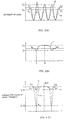
- Figs. 7(A) and 7(B) shows the distribution of light intensity on a wafer, not shown, when the wafer is irradiated through the phase shift mask.
- curves a and b indicates the distribution of light intensity in a portion of the wafer corresponding to a central portion Y2-Y2' of the phase shifting pattern of Fig. 6 and the distribution of light intensity in a portion of the wafer corresponding to an edge portions Y1-Y1' of the phase shifting pattern, respectively.
- a curve c indicates the distribution of maximum light intensity in a portion of the wafer corresponding to a phase shifting portion X1-X1' of the phase shifting pattern.
- light intensity I 2 at a point A on the boundary between the phase shifter and a transparent section, i.e., a shifter edge portion, is lower than light intensity I 1 at a point B in the central portion B of the phase shifter.
- a phase shifting mask according to the present invention comprises a transparent base member, shading layers formed in a pattern selectively on the base member, two kinds of phase shifting layer of a phase difference of 180°, formed in an alternate arrangement between the adjacent shading layers on the base member, respectively, and each having a phase difference of 90° relative to the base member.
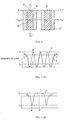
- Fig. 1 is a sectional view of a phase shifting mask of the present invention.
- a transparent base plate 11 shading layers 12, phase shifting layers 13a having a phase difference of 90° relative to the transparent base plate 11, and a phase shifting layers 13b having a phase difference of 270° relative to the transparent base plate 11.
- the phase shifting layers 13b are equivalent to having a phase difference of 90° relative to the transparent base plate 11.
- phase shifting patterns will be described hereinafter.
- Fig. 2 is a top plan view of the phase shifting mask, showing a shift pattern.
- the phase shifting mask has a cyclic pattern of line portions (portions shaded with shading layers) as shading sections, and spacing portions as transmission sections.
- the phase difference between the two kinds of phase shifting layers is 180°.
- curves d and e indicate the distribution of light intensity in the central portion Y4-Y4' and the distribution of light intensity in the edge portion Y3-Y3', respectively, on a wafer, not shown, when the wafer is irradiated through the phase shifting mask with light of wavelength ⁇ .
- a curve f ' indicates the variation of maximum light intensity on the wafer along a line X2-X2' on the phase shifting layer 13a. Pattern intervals are determined so that the contrast on the wafer is 1.0.
- the light intensity I 4 at a boundary point C (at the shifter edge portion) between the phase shifting layer 13a and the transmission section adjacent to the phase shifting layer 13a relative to the light intensity I 3 at the middle point D of the phase shifting layer 13a is on the order of 60%. That is, the light intensity at the boundary point C can be maintained at 0.9 or above in normalized value while the light intensity at the middle point D of the phase shifting layer 13a is maintained on a high level as indicated by a curve g in Fig. 3(C).
- a curve h indicates the distribution of light intensity when the phase shifting layers having a phase difference of 180° relative to the transparent base plate 11 are arranged on alternate shading sections.
- the resolution in the shifter edge portions is improved by the phase shifting mask of the present invention.
- Fig. 4 is a view for evaluation of a resist pattern when the phase shifting mask is used. As is obvious from Fig. 4, the components of the resist pattern are clearly separated, which proves that the resolution is improved.
- phase difference between the two kinds of phase shifting layers is held at 180° by the following means.
- the thickness of the phase shifting layers 13a of 90° in phase is on the order of 240 mm and that of the phase shifting layers 13b of 270° in phase is on the order of 720 mm when they are formed of MgF2 having a refractive index of 1.38 for i-rays of 365 nm in wavelength.
- phase shifting layers 13a of 90° in phase are formed of MgF 2 on the order of 240 mm in thickness and the phase shifting layers 13b of 270° in phase are formed of SiC having a refractive index of 2.83 on the order of 150 mm in thickness.
- the phase shifting mask of the present invention fabricated by forming the two kinds of phase shifting layers having a phase difference on the transparent base plate inverts relatively the phase of light projected on the phase shifting layers to improve resolution. Furthermore, since the two kinds of phase shifting layers are 90° in phase relative to the base plate, the reduction of light intensity in the shifter edge portion is suppressed and shifter edge transfer is suppressed. Accordingly, a phase shifting method according to the present invention is applicable to a process using a positive resist and to a process using a pattern other than patterns in which transmission sections are closed.
- the present invention arranges two kinds of phase shifting layers differing from each other in phase arranged alternately between adjacent shading sections and thereby the phases of light projected on the phase shading mask are inverted relatively to one another. Accordingly, resolution in a photolithographic process is improved.
Landscapes
- Physics & Mathematics (AREA)
- General Physics & Mathematics (AREA)
- Preparing Plates And Mask In Photomechanical Process (AREA)
- Exposure And Positioning Against Photoresist Photosensitive Materials (AREA)
Abstract
Description
- The present invention relates to a phase shifting mask for use in a photolithographic process of forming wiring patterns.
- A phase shifting mask for inverting the phase of light disclosed in "IEEE TRANSACTIONS ON ELECTRON DEVICES, VOLUME ED-29, [NUMBER 12], (December 1982), published in the U.S.A., Page 1828-1836" will be described prior to the description of the present invention.
- The construction and characteristics of this known phase shifting mask are shown in Figs. 5(A) to 5(D). Fig. 5(A) is a sectional view of the phase shifting mask, Fig. 5(B) is a diagram of the amplitude of light on the phase shifting mask, Fig. 5(C) is a diagram of the amplitude of light on a wafer, not shown, and Fig. 5(D) is a diagram of the amplitude of light intensity on a wafer, not shown.
- The phase shifting mask comprises a transparent
glass base plate 1, shadinglayers 2 of chromium (Cr) or chromium oxide (CrO2) formed selectively in areas on one of the major surfaces of thebase plate 1 in a predetermined pattern, and a phase shiftinglayer 3 formed over every other transparent area between theadjacent shading layers 2 on the same surface. - The phase shifting
layer 3 is a single-layer light-transmissive film of an exposed photoresist, SiO2 SOG or MgF2, having a thickness d meeting an expression: d = λ/{(2(n-1)}, where λ is the wavelength of light projected on the phase shifting mask and n is the refractive index ofphase shifting layer 3. - When a wafer, not shown, is irradiated through the phase shifting mask with
light 4 of the wavelength λ, the amplitude of light passed through thephase shifting layer 3 appears on the lower side thereof as shown in Fig. 5(B). That is, the difference between the light passed through thephase shifting layer 3 and the light passed through a transparent section is 180° and consequently the amplitude of the light appears on the wafer as shown in Fig. 5(C) and the light intensity on the wafer is enhanced as shown in Fig. 5(D). - Thus, the light intensity on the waver is enhanced when the
phase shifting layer 3 is formed on every other transparent section of the phase shifting mask having a cyclic pattern as shown in Fig. 5(A) and thereby the contrast of an image formed on the wafer can be improved. - The functions of the phase shifting mask will be described hereinafter with reference to Figs. 6, 7(A) and 7(B).
- Fig. 6 shows a cyclic phase shifting pattern consisting of shading section, i.e., line sections (sections shaded with dots) and transparent sections, i.e., spacing sections (portions of the transparent plate with a phase of 0°). Shifting
layers 3 having a phase difference of 180° relative to the transparent plate are formed alternately in the spacing sections. - Figs. 7(A) and 7(B) shows the distribution of light intensity on a wafer, not shown, when the wafer is irradiated through the phase shift mask. In Fig. 7(A), curves a and b indicates the distribution of light intensity in a portion of the wafer corresponding to a central portion Y2-Y2' of the phase shifting pattern of Fig. 6 and the distribution of light intensity in a portion of the wafer corresponding to an edge portions Y1-Y1' of the phase shifting pattern, respectively.
- In Fig. 7(B), a curve c indicates the distribution of maximum light intensity in a portion of the wafer corresponding to a phase shifting portion X1-X1' of the phase shifting pattern.
- As is obvious from Figs. 7(A) and 7(B), light intensity I2 at a point A on the boundary between the phase shifter and a transparent section, i.e., a shifter edge portion, is lower than light intensity I1 at a point B in the central portion B of the phase shifter.
- A phase shifting mask according to the present invention comprises a transparent base member, shading layers formed in a pattern selectively on the base member, two kinds of phase shifting layer of a phase difference of 180°, formed in an alternate arrangement between the adjacent shading layers on the base member, respectively, and each having a phase difference of 90° relative to the base member.
-
- Fig. 1 is a sectional view of a phase shifting mask of the present invention;
- Fig. 2 is a top plan view of a phase shifting mask of the present invention;
- Fig. 3(A) is a diagram showing the distribution of light intensity on a wafer when a phase shifting mask of the present invention is used;
- Fig. 3(B) is a diagram showing the distribution of light intensity on a wafer when a phase shifting mask of the present invention is used;
- Fig. 3(C) is a diagram showing the distribution of light intensity contrast on a wafer when a phase shifting mask of the present invention is used;
- Fig. 4 is a diagrammatic view for the evaluation of a resist pattern;
- Fig. 5(a) is a sectional view of a prior art phase shifting mask;
- Fig. 5(b) is a diagram showing the amplitude of light on a mask when a prior art phase shifting mask is used;
- Fig. 5(c) is a diagram showing the amplitude of light on a wafer when a prior art phase shifting mask is used;
- Fig. 5(d) is a diagram showing light intensity on a wafer when a prior art phase shifting mask is used;
- Fig. 6 is a top plan view of a prior art phase shifting mask;
- Fig. 7(A) is a diagram showing the distribution of light intensity on a wafer when a prior art phase shifting mask is used; and
- Fig. 7(B is a diagram showing the distribution of light intensity on a wafer when a prior art phase shifting mask is used.
- The present invention will be described hereinafter with reference to Figs. 1 to 3.
- Fig. 1 is a sectional view of a phase shifting mask of the present invention. In Fig. 1, there are shown a transparent base plate 11, shading
layers 12,phase shifting layers 13a having a phase difference of 90° relative to the transparent base plate 11, and aphase shifting layers 13b having a phase difference of 270° relative to the transparent base plate 11. Thephase shifting layers 13b are equivalent to having a phase difference of 90° relative to the transparent base plate 11. - These phase shifting patterns will be described hereinafter.
- Fig. 2 is a top plan view of the phase shifting mask, showing a shift pattern. Referring to Fig. 2, the phase shifting mask has a cyclic pattern of line portions (portions shaded with shading layers) as shading sections, and spacing portions as transmission sections.
Phase shifting layers 13a (phase = 90°) andphase shifting layers 13b (phase = 270°) are arranged alternately on the spacing portions (portions of the transparent base plate having a phase of 0°). The phase difference between the two kinds of phase shifting layers is 180°. - In Fig. 3(A), curves d and e indicate the distribution of light intensity in the central portion Y4-Y4' and the distribution of light intensity in the edge portion Y3-Y3', respectively, on a wafer, not shown, when the wafer is irradiated through the phase shifting mask with light of wavelength λ.
- In Fig. 3(B), a curve f' indicates the variation of maximum light intensity on the wafer along a line X2-X2' on the
phase shifting layer 13a. Pattern intervals are determined so that the contrast on the wafer is 1.0. At that time, as indicated by a curve e in Fig. 3(A), the light intensity I4 at a boundary point C (at the shifter edge portion) between thephase shifting layer 13a and the transmission section adjacent to thephase shifting layer 13a relative to the light intensity I3 at the middle point D of thephase shifting layer 13a is on the order of 60%. That is, the light intensity at the boundary point C can be maintained at 0.9 or above in normalized value while the light intensity at the middle point D of thephase shifting layer 13a is maintained on a high level as indicated by a curve g in Fig. 3(C). - In Fig. 3(C), a curve h indicates the distribution of light intensity when the phase shifting layers having a phase difference of 180° relative to the transparent base plate 11 are arranged on alternate shading sections. As is obvious from the comparative observation of the curve h with the curve g, the resolution in the shifter edge portions is improved by the phase shifting mask of the present invention.
- Fig. 4 is a view for evaluation of a resist pattern when the phase shifting mask is used. As is obvious from Fig. 4, the components of the resist pattern are clearly separated, which proves that the resolution is improved.
- In the present invention, the phase difference between the two kinds of phase shifting layers is held at 180° by the following means.
- Concretely, the thickness of the
phase shifting layers 13a of 90° in phase is on the order of 240 mm and that of thephase shifting layers 13b of 270° in phase is on the order of 720 mm when they are formed of MgF2 having a refractive index of 1.38 for i-rays of 365 nm in wavelength. - It is also possible that the
phase shifting layers 13a of 90° in phase are formed of MgF2 on the order of 240 mm in thickness and thephase shifting layers 13b of 270° in phase are formed of SiC having a refractive index of 2.83 on the order of 150 mm in thickness. - As is apparent from the foregoing description, the phase shifting mask of the present invention fabricated by forming the two kinds of phase shifting layers having a phase difference on the transparent base plate inverts relatively the phase of light projected on the phase shifting layers to improve resolution. Furthermore, since the two kinds of phase shifting layers are 90° in phase relative to the base plate, the reduction of light intensity in the shifter edge portion is suppressed and shifter edge transfer is suppressed. Accordingly, a phase shifting method according to the present invention is applicable to a process using a positive resist and to a process using a pattern other than patterns in which transmission sections are closed.
- The present invention arranges two kinds of phase shifting layers differing from each other in phase arranged alternately between adjacent shading sections and thereby the phases of light projected on the phase shading mask are inverted relatively to one another. Accordingly, resolution in a photolithographic process is improved.
Claims (3)
- A phase shifting mask comprising;a transparent base member having a major surface;shading layers capable of intercepting light, formed selectively on the major surface of the base member; andfirst and second phase shifting layers formed alternately on the major surface of the base member between the adjacent shading patterns to create a phase difference between light transmitted therethrough;wherein the phase difference between light transmitted through the first phase shifting layers and light transmitted through the base member is 90°, the phase difference between light transmitted through the second phase shifting layers and light transmitted through the base member is 270°, and the phase difference between light transmitted through the first phase shifting layers and light transmitted through the second phase shifting layers is 180°.
- A phase shifting mask according to claim 1, wherein said first and second phase shifting layers comprise magnesium fluoride.
- A phase shifting mask according to claim 3, wherein said first phase shifting layer has a thickness of 240nm, said second phase shifting layer has a thickness of 720nm, and the light passing through the phase shifting mask has i-rays of 365nm in wave length.
Applications Claiming Priority (3)
| Application Number | Priority Date | Filing Date | Title |
|---|---|---|---|
| JP161239/90 | 1990-06-21 | ||
| JP16123990 | 1990-06-21 | ||
| PCT/JP1991/000817 WO1991020018A1 (en) | 1990-06-21 | 1991-06-19 | Mask for shifting phase |
Publications (3)
| Publication Number | Publication Date |
|---|---|
| EP0535229A1 EP0535229A1 (en) | 1993-04-07 |
| EP0535229A4 EP0535229A4 (en) | 1993-07-28 |
| EP0535229B1 true EP0535229B1 (en) | 1997-02-05 |
Family
ID=15731291
Family Applications (1)
| Application Number | Title | Priority Date | Filing Date |
|---|---|---|---|
| EP91910858A Expired - Lifetime EP0535229B1 (en) | 1990-06-21 | 1991-06-19 | Mask for shifting phase |
Country Status (5)
| Country | Link |
|---|---|
| US (1) | US5342713A (en) |
| EP (1) | EP0535229B1 (en) |
| KR (1) | KR0153287B1 (en) |
| DE (1) | DE69124604T2 (en) |
| WO (1) | WO1991020018A1 (en) |
Families Citing this family (16)
| Publication number | Priority date | Publication date | Assignee | Title |
|---|---|---|---|---|
| US5328785A (en) * | 1992-02-10 | 1994-07-12 | Litel Instruments | High power phase masks for imaging systems |
| US5789118A (en) * | 1992-08-21 | 1998-08-04 | Intel Corporation | Method and apparatus for precision determination of phase-shift in a phase-shifted reticle |
| US5700602A (en) * | 1992-08-21 | 1997-12-23 | Intel Corporation | Method and apparatus for precision determination of phase-shift in a phase-shifted reticle |
| US5300379A (en) * | 1992-08-21 | 1994-04-05 | Intel Corporation | Method of fabrication of inverted phase-shifted reticle |
| US5302477A (en) * | 1992-08-21 | 1994-04-12 | Intel Corporation | Inverted phase-shifted reticle |
| KR0143340B1 (en) * | 1994-09-09 | 1998-08-17 | 김주용 | Phase shift mask |
| US5595843A (en) * | 1995-03-30 | 1997-01-21 | Intel Corporation | Layout methodology, mask set, and patterning method for phase-shifting lithography |
| KR960042202A (en) * | 1995-05-19 | 1996-12-21 | 김주용 | Reticle for Semiconductor Pattern Formation |
| KR0147665B1 (en) * | 1995-09-13 | 1998-10-01 | 김광호 | Changing illumination method reflection mirror and making method used thereof |
| JP3588212B2 (en) * | 1996-12-20 | 2004-11-10 | 株式会社ルネサステクノロジ | Exposure mask, method for manufacturing the same, and method for manufacturing semiconductor device |
| US6034877A (en) * | 1998-06-08 | 2000-03-07 | International Business Machines Corporation | Semiconductor memory array having sublithographic spacing between adjacement trenches and method for making the same |
| US6277527B1 (en) | 1999-04-29 | 2001-08-21 | International Business Machines Corporation | Method of making a twin alternating phase shift mask |
| US6090633A (en) * | 1999-09-22 | 2000-07-18 | International Business Machines Corporation | Multiple-plane pair thin-film structure and process of manufacture |
| DE19948570C2 (en) * | 1999-10-08 | 2001-07-26 | Infineon Technologies Ag | Arrangement for wiring conductor tracks |
| US6493866B1 (en) * | 2000-06-30 | 2002-12-10 | Synopsys, Inc. | Phase-shift lithography mapping and apparatus |
| KR100446306B1 (en) * | 2002-08-28 | 2004-09-01 | 삼성전자주식회사 | Mask for highly integrated circuit device fabrication, generating method of their layout, fabrication method thereof, and fabrication method for highly integrated circuit using the same |
Family Cites Families (6)
| Publication number | Priority date | Publication date | Assignee | Title |
|---|---|---|---|---|
| US4360586A (en) * | 1979-05-29 | 1982-11-23 | Massachusetts Institute Of Technology | Spatial period division exposing |
| EP0090924B1 (en) * | 1982-04-05 | 1987-11-11 | International Business Machines Corporation | Method of increasing the image resolution of a transmitting mask and improved masks for performing the method |
| JPS6259296A (en) * | 1985-09-10 | 1987-03-14 | Green Cross Corp:The | Peptide derivative |
| US4890309A (en) * | 1987-02-25 | 1989-12-26 | Massachusetts Institute Of Technology | Lithography mask with a π-phase shifting attenuator |
| JP2564337B2 (en) * | 1987-12-04 | 1996-12-18 | 株式会社日立製作所 | Mask and pattern transfer method and semiconductor integrated circuit manufacturing method |
| JP2865685B2 (en) * | 1988-03-16 | 1999-03-08 | 株式会社日立製作所 | Method for manufacturing semiconductor device |
-
1991
- 1991-06-19 EP EP91910858A patent/EP0535229B1/en not_active Expired - Lifetime
- 1991-06-19 WO PCT/JP1991/000817 patent/WO1991020018A1/en not_active Ceased
- 1991-06-19 KR KR1019920703253A patent/KR0153287B1/en not_active Expired - Fee Related
- 1991-06-19 US US07/949,824 patent/US5342713A/en not_active Expired - Lifetime
- 1991-06-19 DE DE69124604T patent/DE69124604T2/en not_active Expired - Fee Related
Also Published As
| Publication number | Publication date |
|---|---|
| EP0535229A4 (en) | 1993-07-28 |
| DE69124604D1 (en) | 1997-03-20 |
| EP0535229A1 (en) | 1993-04-07 |
| US5342713A (en) | 1994-08-30 |
| KR930701769A (en) | 1993-06-12 |
| DE69124604T2 (en) | 1997-09-04 |
| KR0153287B1 (en) | 1998-11-02 |
| WO1991020018A1 (en) | 1991-12-26 |
Similar Documents
| Publication | Publication Date | Title |
|---|---|---|
| US5342713A (en) | Phase shifting mask | |
| US5565286A (en) | Combined attenuated-alternating phase shifting mask structure and fabrication methods therefor | |
| US5858580A (en) | Phase shifting circuit manufacture method and apparatus | |
| EP0927381B1 (en) | Phase shifting circuit manufacturing method and device | |
| EP0532040B1 (en) | Discrete phase shift mask writing | |
| US20010028985A1 (en) | Phase shifting circuit manufacture method and apparatus | |
| JP2540011B2 (en) | Phase shift mask | |
| US6558854B2 (en) | Process for forming features on a semiconductor wafer using a phase shifting mask that can be used with two different wavelengths of light | |
| KR100236045B1 (en) | Phase inversion mask and manufacturing method thereof | |
| EP0567419A2 (en) | A shifter-based rim phase shifting structure and process to fabricate the same | |
| WO2005103820A1 (en) | Levenson type phase shift mask and production method therefor | |
| US5942355A (en) | Method of fabricating a phase-shifting semiconductor photomask | |
| KR100207473B1 (en) | Phase shift mask manufacturing method | |
| JP2781322B2 (en) | Photomask manufacturing method | |
| JPH07253655A (en) | Exposure mask | |
| US6524751B1 (en) | Reticle design for alternating phase shift mask | |
| JP2976194B2 (en) | Phase shift mask structure and manufacturing method | |
| JP2724982B2 (en) | Method for manufacturing multiple phase shift mask | |
| JPH07140638A (en) | Phase inversion mask manufacturing method | |
| JPH05197125A (en) | Phase shift mask | |
| KR100190115B1 (en) | Phase shift mask and its manufacturing method | |
| KR0151262B1 (en) | Method of multistage phase shift mask | |
| KR100215880B1 (en) | Manufacturing method of phase inversion mask | |
| KR19990065307A (en) | Phase reversal mask of semiconductor device and manufacturing method thereof | |
| JPH03245145A (en) | Projecting and exposing method |
Legal Events
| Date | Code | Title | Description |
|---|---|---|---|
| PUAI | Public reference made under article 153(3) epc to a published international application that has entered the european phase |
Free format text: ORIGINAL CODE: 0009012 |
|
| 17P | Request for examination filed |
Effective date: 19930121 |
|
| AK | Designated contracting states |
Kind code of ref document: A1 Designated state(s): DE FR NL |
|
| A4 | Supplementary search report drawn up and despatched |
Effective date: 19930609 |
|
| AK | Designated contracting states |
Kind code of ref document: A4 Designated state(s): DE FR NL |
|
| 17Q | First examination report despatched |
Effective date: 19940418 |
|
| GRAG | Despatch of communication of intention to grant |
Free format text: ORIGINAL CODE: EPIDOS AGRA |
|
| GRAG | Despatch of communication of intention to grant |
Free format text: ORIGINAL CODE: EPIDOS AGRA |
|
| GRAH | Despatch of communication of intention to grant a patent |
Free format text: ORIGINAL CODE: EPIDOS IGRA |
|
| GRAH | Despatch of communication of intention to grant a patent |
Free format text: ORIGINAL CODE: EPIDOS IGRA |
|
| GRAA | (expected) grant |
Free format text: ORIGINAL CODE: 0009210 |
|
| AK | Designated contracting states |
Kind code of ref document: B1 Designated state(s): DE FR NL |
|
| REF | Corresponds to: |
Ref document number: 69124604 Country of ref document: DE Date of ref document: 19970320 |
|
| ET | Fr: translation filed | ||
| PLBE | No opposition filed within time limit |
Free format text: ORIGINAL CODE: 0009261 |
|
| STAA | Information on the status of an ep patent application or granted ep patent |
Free format text: STATUS: NO OPPOSITION FILED WITHIN TIME LIMIT |
|
| 26N | No opposition filed | ||
| PGFP | Annual fee paid to national office [announced via postgrant information from national office to epo] |
Ref country code: FR Payment date: 20060608 Year of fee payment: 16 |
|
| PGFP | Annual fee paid to national office [announced via postgrant information from national office to epo] |
Ref country code: NL Payment date: 20060615 Year of fee payment: 16 Ref country code: DE Payment date: 20060615 Year of fee payment: 16 |
|
| NLV4 | Nl: lapsed or anulled due to non-payment of the annual fee |
Effective date: 20080101 |
|
| REG | Reference to a national code |
Ref country code: FR Ref legal event code: ST Effective date: 20080229 |
|
| PG25 | Lapsed in a contracting state [announced via postgrant information from national office to epo] |
Ref country code: NL Free format text: LAPSE BECAUSE OF NON-PAYMENT OF DUE FEES Effective date: 20080101 Ref country code: DE Free format text: LAPSE BECAUSE OF NON-PAYMENT OF DUE FEES Effective date: 20080101 |
|
| PG25 | Lapsed in a contracting state [announced via postgrant information from national office to epo] |
Ref country code: FR Free format text: LAPSE BECAUSE OF NON-PAYMENT OF DUE FEES Effective date: 20070702 |