EP0533164B1 - Ball bonding method and apparatus for using the same - Google Patents
Ball bonding method and apparatus for using the same Download PDFInfo
- Publication number
- EP0533164B1 EP0533164B1 EP92115937A EP92115937A EP0533164B1 EP 0533164 B1 EP0533164 B1 EP 0533164B1 EP 92115937 A EP92115937 A EP 92115937A EP 92115937 A EP92115937 A EP 92115937A EP 0533164 B1 EP0533164 B1 EP 0533164B1
- Authority
- EP
- European Patent Office
- Prior art keywords
- bonding
- wire
- free
- singeing
- ball
- Prior art date
- Legal status (The legal status is an assumption and is not a legal conclusion. Google has not performed a legal analysis and makes no representation as to the accuracy of the status listed.)
- Expired - Lifetime
Links
Images
Classifications
-
- H—ELECTRICITY
- H01—ELECTRIC ELEMENTS
- H01L—SEMICONDUCTOR DEVICES NOT COVERED BY CLASS H10
- H01L24/00—Arrangements for connecting or disconnecting semiconductor or solid-state bodies; Methods or apparatus related thereto
- H01L24/80—Methods for connecting semiconductor or other solid state bodies using means for bonding being attached to, or being formed on, the surface to be connected
- H01L24/85—Methods for connecting semiconductor or other solid state bodies using means for bonding being attached to, or being formed on, the surface to be connected using a wire connector
-
- B—PERFORMING OPERATIONS; TRANSPORTING
- B23—MACHINE TOOLS; METAL-WORKING NOT OTHERWISE PROVIDED FOR
- B23K—SOLDERING OR UNSOLDERING; WELDING; CLADDING OR PLATING BY SOLDERING OR WELDING; CUTTING BY APPLYING HEAT LOCALLY, e.g. FLAME CUTTING; WORKING BY LASER BEAM
- B23K20/00—Non-electric welding by applying impact or other pressure, with or without the application of heat, e.g. cladding or plating
- B23K20/002—Non-electric welding by applying impact or other pressure, with or without the application of heat, e.g. cladding or plating specially adapted for particular articles or work
- B23K20/004—Wire welding
- B23K20/005—Capillary welding
- B23K20/007—Ball bonding
-
- H—ELECTRICITY
- H01—ELECTRIC ELEMENTS
- H01L—SEMICONDUCTOR DEVICES NOT COVERED BY CLASS H10
- H01L21/00—Processes or apparatus adapted for the manufacture or treatment of semiconductor or solid state devices or of parts thereof
- H01L21/02—Manufacture or treatment of semiconductor devices or of parts thereof
- H01L21/04—Manufacture or treatment of semiconductor devices or of parts thereof the devices having at least one potential-jump barrier or surface barrier, e.g. PN junction, depletion layer or carrier concentration layer
- H01L21/50—Assembly of semiconductor devices using processes or apparatus not provided for in a single one of the subgroups H01L21/06 - H01L21/326, e.g. sealing of a cap to a base of a container
- H01L21/60—Attaching or detaching leads or other conductive members, to be used for carrying current to or from the device in operation
-
- H—ELECTRICITY
- H01—ELECTRIC ELEMENTS
- H01L—SEMICONDUCTOR DEVICES NOT COVERED BY CLASS H10
- H01L24/00—Arrangements for connecting or disconnecting semiconductor or solid-state bodies; Methods or apparatus related thereto
- H01L24/74—Apparatus for manufacturing arrangements for connecting or disconnecting semiconductor or solid-state bodies
- H01L24/78—Apparatus for connecting with wire connectors
-
- H—ELECTRICITY
- H01—ELECTRIC ELEMENTS
- H01L—SEMICONDUCTOR DEVICES NOT COVERED BY CLASS H10
- H01L2224/00—Indexing scheme for arrangements for connecting or disconnecting semiconductor or solid-state bodies and methods related thereto as covered by H01L24/00
- H01L2224/01—Means for bonding being attached to, or being formed on, the surface to be connected, e.g. chip-to-package, die-attach, "first-level" interconnects; Manufacturing methods related thereto
- H01L2224/42—Wire connectors; Manufacturing methods related thereto
- H01L2224/44—Structure, shape, material or disposition of the wire connectors prior to the connecting process
- H01L2224/45—Structure, shape, material or disposition of the wire connectors prior to the connecting process of an individual wire connector
- H01L2224/45001—Core members of the connector
- H01L2224/45099—Material
- H01L2224/451—Material with a principal constituent of the material being a metal or a metalloid, e.g. boron (B), silicon (Si), germanium (Ge), arsenic (As), antimony (Sb), tellurium (Te) and polonium (Po), and alloys thereof
- H01L2224/45138—Material with a principal constituent of the material being a metal or a metalloid, e.g. boron (B), silicon (Si), germanium (Ge), arsenic (As), antimony (Sb), tellurium (Te) and polonium (Po), and alloys thereof the principal constituent melting at a temperature of greater than or equal to 950°C and less than 1550°C
- H01L2224/45144—Gold (Au) as principal constituent
-
- H—ELECTRICITY
- H01—ELECTRIC ELEMENTS
- H01L—SEMICONDUCTOR DEVICES NOT COVERED BY CLASS H10
- H01L2224/00—Indexing scheme for arrangements for connecting or disconnecting semiconductor or solid-state bodies and methods related thereto as covered by H01L24/00
- H01L2224/01—Means for bonding being attached to, or being formed on, the surface to be connected, e.g. chip-to-package, die-attach, "first-level" interconnects; Manufacturing methods related thereto
- H01L2224/42—Wire connectors; Manufacturing methods related thereto
- H01L2224/47—Structure, shape, material or disposition of the wire connectors after the connecting process
- H01L2224/48—Structure, shape, material or disposition of the wire connectors after the connecting process of an individual wire connector
- H01L2224/4805—Shape
- H01L2224/4809—Loop shape
- H01L2224/48091—Arched
-
- H—ELECTRICITY
- H01—ELECTRIC ELEMENTS
- H01L—SEMICONDUCTOR DEVICES NOT COVERED BY CLASS H10
- H01L2224/00—Indexing scheme for arrangements for connecting or disconnecting semiconductor or solid-state bodies and methods related thereto as covered by H01L24/00
- H01L2224/01—Means for bonding being attached to, or being formed on, the surface to be connected, e.g. chip-to-package, die-attach, "first-level" interconnects; Manufacturing methods related thereto
- H01L2224/42—Wire connectors; Manufacturing methods related thereto
- H01L2224/47—Structure, shape, material or disposition of the wire connectors after the connecting process
- H01L2224/48—Structure, shape, material or disposition of the wire connectors after the connecting process of an individual wire connector
- H01L2224/481—Disposition
- H01L2224/48151—Connecting between a semiconductor or solid-state body and an item not being a semiconductor or solid-state body, e.g. chip-to-substrate, chip-to-passive
- H01L2224/48221—Connecting between a semiconductor or solid-state body and an item not being a semiconductor or solid-state body, e.g. chip-to-substrate, chip-to-passive the body and the item being stacked
- H01L2224/48225—Connecting between a semiconductor or solid-state body and an item not being a semiconductor or solid-state body, e.g. chip-to-substrate, chip-to-passive the body and the item being stacked the item being non-metallic, e.g. insulating substrate with or without metallisation
- H01L2224/48227—Connecting between a semiconductor or solid-state body and an item not being a semiconductor or solid-state body, e.g. chip-to-substrate, chip-to-passive the body and the item being stacked the item being non-metallic, e.g. insulating substrate with or without metallisation connecting the wire to a bond pad of the item
-
- H—ELECTRICITY
- H01—ELECTRIC ELEMENTS
- H01L—SEMICONDUCTOR DEVICES NOT COVERED BY CLASS H10
- H01L2224/00—Indexing scheme for arrangements for connecting or disconnecting semiconductor or solid-state bodies and methods related thereto as covered by H01L24/00
- H01L2224/01—Means for bonding being attached to, or being formed on, the surface to be connected, e.g. chip-to-package, die-attach, "first-level" interconnects; Manufacturing methods related thereto
- H01L2224/42—Wire connectors; Manufacturing methods related thereto
- H01L2224/47—Structure, shape, material or disposition of the wire connectors after the connecting process
- H01L2224/48—Structure, shape, material or disposition of the wire connectors after the connecting process of an individual wire connector
- H01L2224/481—Disposition
- H01L2224/48151—Connecting between a semiconductor or solid-state body and an item not being a semiconductor or solid-state body, e.g. chip-to-substrate, chip-to-passive
- H01L2224/48221—Connecting between a semiconductor or solid-state body and an item not being a semiconductor or solid-state body, e.g. chip-to-substrate, chip-to-passive the body and the item being stacked
- H01L2224/48245—Connecting between a semiconductor or solid-state body and an item not being a semiconductor or solid-state body, e.g. chip-to-substrate, chip-to-passive the body and the item being stacked the item being metallic
- H01L2224/48247—Connecting between a semiconductor or solid-state body and an item not being a semiconductor or solid-state body, e.g. chip-to-substrate, chip-to-passive the body and the item being stacked the item being metallic connecting the wire to a bond pad of the item
-
- H—ELECTRICITY
- H01—ELECTRIC ELEMENTS
- H01L—SEMICONDUCTOR DEVICES NOT COVERED BY CLASS H10
- H01L2224/00—Indexing scheme for arrangements for connecting or disconnecting semiconductor or solid-state bodies and methods related thereto as covered by H01L24/00
- H01L2224/01—Means for bonding being attached to, or being formed on, the surface to be connected, e.g. chip-to-package, die-attach, "first-level" interconnects; Manufacturing methods related thereto
- H01L2224/42—Wire connectors; Manufacturing methods related thereto
- H01L2224/47—Structure, shape, material or disposition of the wire connectors after the connecting process
- H01L2224/48—Structure, shape, material or disposition of the wire connectors after the connecting process of an individual wire connector
- H01L2224/484—Connecting portions
- H01L2224/48463—Connecting portions the connecting portion on the bonding area of the semiconductor or solid-state body being a ball bond
- H01L2224/48464—Connecting portions the connecting portion on the bonding area of the semiconductor or solid-state body being a ball bond the other connecting portion not on the bonding area also being a ball bond, i.e. ball-to-ball
-
- H—ELECTRICITY
- H01—ELECTRIC ELEMENTS
- H01L—SEMICONDUCTOR DEVICES NOT COVERED BY CLASS H10
- H01L2224/00—Indexing scheme for arrangements for connecting or disconnecting semiconductor or solid-state bodies and methods related thereto as covered by H01L24/00
- H01L2224/01—Means for bonding being attached to, or being formed on, the surface to be connected, e.g. chip-to-package, die-attach, "first-level" interconnects; Manufacturing methods related thereto
- H01L2224/42—Wire connectors; Manufacturing methods related thereto
- H01L2224/47—Structure, shape, material or disposition of the wire connectors after the connecting process
- H01L2224/48—Structure, shape, material or disposition of the wire connectors after the connecting process of an individual wire connector
- H01L2224/484—Connecting portions
- H01L2224/48463—Connecting portions the connecting portion on the bonding area of the semiconductor or solid-state body being a ball bond
- H01L2224/48465—Connecting portions the connecting portion on the bonding area of the semiconductor or solid-state body being a ball bond the other connecting portion not on the bonding area being a wedge bond, i.e. ball-to-wedge, regular stitch
-
- H—ELECTRICITY
- H01—ELECTRIC ELEMENTS
- H01L—SEMICONDUCTOR DEVICES NOT COVERED BY CLASS H10
- H01L2224/00—Indexing scheme for arrangements for connecting or disconnecting semiconductor or solid-state bodies and methods related thereto as covered by H01L24/00
- H01L2224/74—Apparatus for manufacturing arrangements for connecting or disconnecting semiconductor or solid-state bodies and for methods related thereto
- H01L2224/78—Apparatus for connecting with wire connectors
- H01L2224/7825—Means for applying energy, e.g. heating means
- H01L2224/783—Means for applying energy, e.g. heating means by means of pressure
- H01L2224/78301—Capillary
-
- H—ELECTRICITY
- H01—ELECTRIC ELEMENTS
- H01L—SEMICONDUCTOR DEVICES NOT COVERED BY CLASS H10
- H01L2224/00—Indexing scheme for arrangements for connecting or disconnecting semiconductor or solid-state bodies and methods related thereto as covered by H01L24/00
- H01L2224/80—Methods for connecting semiconductor or other solid state bodies using means for bonding being attached to, or being formed on, the surface to be connected
- H01L2224/85—Methods for connecting semiconductor or other solid state bodies using means for bonding being attached to, or being formed on, the surface to be connected using a wire connector
- H01L2224/85009—Pre-treatment of the connector or the bonding area
- H01L2224/8503—Reshaping, e.g. forming the ball or the wedge of the wire connector
- H01L2224/85035—Reshaping, e.g. forming the ball or the wedge of the wire connector by heating means, e.g. "free-air-ball"
- H01L2224/85045—Reshaping, e.g. forming the ball or the wedge of the wire connector by heating means, e.g. "free-air-ball" using a corona discharge, e.g. electronic flame off [EFO]
-
- H—ELECTRICITY
- H01—ELECTRIC ELEMENTS
- H01L—SEMICONDUCTOR DEVICES NOT COVERED BY CLASS H10
- H01L2224/00—Indexing scheme for arrangements for connecting or disconnecting semiconductor or solid-state bodies and methods related thereto as covered by H01L24/00
- H01L2224/80—Methods for connecting semiconductor or other solid state bodies using means for bonding being attached to, or being formed on, the surface to be connected
- H01L2224/85—Methods for connecting semiconductor or other solid state bodies using means for bonding being attached to, or being formed on, the surface to be connected using a wire connector
- H01L2224/851—Methods for connecting semiconductor or other solid state bodies using means for bonding being attached to, or being formed on, the surface to be connected using a wire connector the connector being supplied to the parts to be connected in the bonding apparatus
-
- H—ELECTRICITY
- H01—ELECTRIC ELEMENTS
- H01L—SEMICONDUCTOR DEVICES NOT COVERED BY CLASS H10
- H01L2224/00—Indexing scheme for arrangements for connecting or disconnecting semiconductor or solid-state bodies and methods related thereto as covered by H01L24/00
- H01L2224/80—Methods for connecting semiconductor or other solid state bodies using means for bonding being attached to, or being formed on, the surface to be connected
- H01L2224/85—Methods for connecting semiconductor or other solid state bodies using means for bonding being attached to, or being formed on, the surface to be connected using a wire connector
- H01L2224/8512—Aligning
- H01L2224/85148—Aligning involving movement of a part of the bonding apparatus
- H01L2224/85169—Aligning involving movement of a part of the bonding apparatus being the upper part of the bonding apparatus, i.e. bonding head, e.g. capillary or wedge
- H01L2224/8518—Translational movements
- H01L2224/85181—Translational movements connecting first on the semiconductor or solid-state body, i.e. on-chip, regular stitch
-
- H—ELECTRICITY
- H01—ELECTRIC ELEMENTS
- H01L—SEMICONDUCTOR DEVICES NOT COVERED BY CLASS H10
- H01L2224/00—Indexing scheme for arrangements for connecting or disconnecting semiconductor or solid-state bodies and methods related thereto as covered by H01L24/00
- H01L2224/80—Methods for connecting semiconductor or other solid state bodies using means for bonding being attached to, or being formed on, the surface to be connected
- H01L2224/85—Methods for connecting semiconductor or other solid state bodies using means for bonding being attached to, or being formed on, the surface to be connected using a wire connector
- H01L2224/852—Applying energy for connecting
- H01L2224/85201—Compression bonding
- H01L2224/85205—Ultrasonic bonding
-
- H—ELECTRICITY
- H01—ELECTRIC ELEMENTS
- H01L—SEMICONDUCTOR DEVICES NOT COVERED BY CLASS H10
- H01L2224/00—Indexing scheme for arrangements for connecting or disconnecting semiconductor or solid-state bodies and methods related thereto as covered by H01L24/00
- H01L2224/80—Methods for connecting semiconductor or other solid state bodies using means for bonding being attached to, or being formed on, the surface to be connected
- H01L2224/85—Methods for connecting semiconductor or other solid state bodies using means for bonding being attached to, or being formed on, the surface to be connected using a wire connector
- H01L2224/859—Methods for connecting semiconductor or other solid state bodies using means for bonding being attached to, or being formed on, the surface to be connected using a wire connector involving monitoring, e.g. feedback loop
-
- H—ELECTRICITY
- H01—ELECTRIC ELEMENTS
- H01L—SEMICONDUCTOR DEVICES NOT COVERED BY CLASS H10
- H01L24/00—Arrangements for connecting or disconnecting semiconductor or solid-state bodies; Methods or apparatus related thereto
- H01L24/01—Means for bonding being attached to, or being formed on, the surface to be connected, e.g. chip-to-package, die-attach, "first-level" interconnects; Manufacturing methods related thereto
- H01L24/42—Wire connectors; Manufacturing methods related thereto
- H01L24/44—Structure, shape, material or disposition of the wire connectors prior to the connecting process
- H01L24/45—Structure, shape, material or disposition of the wire connectors prior to the connecting process of an individual wire connector
-
- H—ELECTRICITY
- H01—ELECTRIC ELEMENTS
- H01L—SEMICONDUCTOR DEVICES NOT COVERED BY CLASS H10
- H01L24/00—Arrangements for connecting or disconnecting semiconductor or solid-state bodies; Methods or apparatus related thereto
- H01L24/01—Means for bonding being attached to, or being formed on, the surface to be connected, e.g. chip-to-package, die-attach, "first-level" interconnects; Manufacturing methods related thereto
- H01L24/42—Wire connectors; Manufacturing methods related thereto
- H01L24/47—Structure, shape, material or disposition of the wire connectors after the connecting process
- H01L24/48—Structure, shape, material or disposition of the wire connectors after the connecting process of an individual wire connector
-
- H—ELECTRICITY
- H01—ELECTRIC ELEMENTS
- H01L—SEMICONDUCTOR DEVICES NOT COVERED BY CLASS H10
- H01L2924/00—Indexing scheme for arrangements or methods for connecting or disconnecting semiconductor or solid-state bodies as covered by H01L24/00
- H01L2924/01—Chemical elements
- H01L2924/01005—Boron [B]
-
- H—ELECTRICITY
- H01—ELECTRIC ELEMENTS
- H01L—SEMICONDUCTOR DEVICES NOT COVERED BY CLASS H10
- H01L2924/00—Indexing scheme for arrangements or methods for connecting or disconnecting semiconductor or solid-state bodies as covered by H01L24/00
- H01L2924/01—Chemical elements
- H01L2924/01006—Carbon [C]
-
- H—ELECTRICITY
- H01—ELECTRIC ELEMENTS
- H01L—SEMICONDUCTOR DEVICES NOT COVERED BY CLASS H10
- H01L2924/00—Indexing scheme for arrangements or methods for connecting or disconnecting semiconductor or solid-state bodies as covered by H01L24/00
- H01L2924/01—Chemical elements
- H01L2924/01023—Vanadium [V]
-
- H—ELECTRICITY
- H01—ELECTRIC ELEMENTS
- H01L—SEMICONDUCTOR DEVICES NOT COVERED BY CLASS H10
- H01L2924/00—Indexing scheme for arrangements or methods for connecting or disconnecting semiconductor or solid-state bodies as covered by H01L24/00
- H01L2924/01—Chemical elements
- H01L2924/01033—Arsenic [As]
-
- H—ELECTRICITY
- H01—ELECTRIC ELEMENTS
- H01L—SEMICONDUCTOR DEVICES NOT COVERED BY CLASS H10
- H01L2924/00—Indexing scheme for arrangements or methods for connecting or disconnecting semiconductor or solid-state bodies as covered by H01L24/00
- H01L2924/01—Chemical elements
- H01L2924/0105—Tin [Sn]
-
- H—ELECTRICITY
- H01—ELECTRIC ELEMENTS
- H01L—SEMICONDUCTOR DEVICES NOT COVERED BY CLASS H10
- H01L2924/00—Indexing scheme for arrangements or methods for connecting or disconnecting semiconductor or solid-state bodies as covered by H01L24/00
- H01L2924/01—Chemical elements
- H01L2924/01075—Rhenium [Re]
-
- H—ELECTRICITY
- H01—ELECTRIC ELEMENTS
- H01L—SEMICONDUCTOR DEVICES NOT COVERED BY CLASS H10
- H01L2924/00—Indexing scheme for arrangements or methods for connecting or disconnecting semiconductor or solid-state bodies as covered by H01L24/00
- H01L2924/01—Chemical elements
- H01L2924/01079—Gold [Au]
-
- H—ELECTRICITY
- H01—ELECTRIC ELEMENTS
- H01L—SEMICONDUCTOR DEVICES NOT COVERED BY CLASS H10
- H01L2924/00—Indexing scheme for arrangements or methods for connecting or disconnecting semiconductor or solid-state bodies as covered by H01L24/00
- H01L2924/01—Chemical elements
- H01L2924/01082—Lead [Pb]
-
- H—ELECTRICITY
- H01—ELECTRIC ELEMENTS
- H01L—SEMICONDUCTOR DEVICES NOT COVERED BY CLASS H10
- H01L2924/00—Indexing scheme for arrangements or methods for connecting or disconnecting semiconductor or solid-state bodies as covered by H01L24/00
- H01L2924/013—Alloys
- H01L2924/014—Solder alloys
-
- H—ELECTRICITY
- H01—ELECTRIC ELEMENTS
- H01L—SEMICONDUCTOR DEVICES NOT COVERED BY CLASS H10
- H01L2924/00—Indexing scheme for arrangements or methods for connecting or disconnecting semiconductor or solid-state bodies as covered by H01L24/00
- H01L2924/19—Details of hybrid assemblies other than the semiconductor or other solid state devices to be connected
- H01L2924/1901—Structure
- H01L2924/1904—Component type
- H01L2924/19042—Component type being an inductor
Landscapes
- Engineering & Computer Science (AREA)
- Computer Hardware Design (AREA)
- Microelectronics & Electronic Packaging (AREA)
- Power Engineering (AREA)
- Manufacturing & Machinery (AREA)
- Mechanical Engineering (AREA)
- Physics & Mathematics (AREA)
- Condensed Matter Physics & Semiconductors (AREA)
- General Physics & Mathematics (AREA)
- Wire Bonding (AREA)
- Die Bonding (AREA)
- Container, Conveyance, Adherence, Positioning, Of Wafer (AREA)
Abstract
Description
Die Erfindung betrifft ein Ball-Bondverfahren, wie ein Golddraht-Bondverfahren, nach dem Oberbegriff des Anspruches 1 und eine Vorrichtung zur Durchführung des Verfahrens nach dem Oberbegriff des Anspruches 3.The invention relates to a ball bonding method, such as a Gold wire bonding process, according to the preamble of the claim 1 and an apparatus for performing the method according to the preamble of claim 3.
Ein solches Ball-Bondverfahren ist aus der US-A-4,586,642 bekannt. Bei diesem Verfahren wird zunächst der Bondkopf bzw. eine diesem zugeordnete Bond-Kapillare mit einer abgeflammten Bonddraht-Kugel (Ball) am unteren, freien Ende eines Bonddrahtes aus einer hochgefahrenen Ausgangsposition auf eine erste Bondstelle positioniert und abgesenkt. Sodann wird der Ball unter Wärmezugabe, definiertem Anpreßdruck und/oder Ultraschallunterstützung auf der ersten Bondstelle aufgeschweißt. Hiernach wird die Bondkapillare hochgefahren und eine Bonddraht-Schleife oder loop gebildet. Anschließend wird der Bonddraht wiederum unter Wärmezugabe, definiertem Anpreßdruck und/oder Ultraschallunterstützung an einer zweiten Bondstelle aufgeschweißt. Daraufhin wird der Bondkopf bzw. die Bond-Kapillare in eine vorgegebene tail-length-Position hochgefahren, der Bonddraht durch Ausübung eines Zuges auf diesen mittels einer am Bonddraht angreifenden Drahtklammer abgerissen und anschließend die Bond-Kapillare in die Ausgangsposition angehoben. Letztlich wird das freie Bonddrahtende unter Ausbildung eines neuen Balls abgeflammt, so daß dieses Ball-Bondverfahren erneut durchgeführt werden kann.Such a ball bonding process is known from US-A-4,586,642 known. In this process, the bondhead is first used or a bond capillary assigned to it with a flamed one Bond wire ball (ball) at the lower, free end of a Bond wire from a raised starting position positioned on a first bond site and lowered. Then the ball is added heat, defined contact pressure and / or ultrasound support on the first Bond point welded on. After that the bond capillary started up and a bond wire loop or loop formed. Then the bond wire is again heated, defined contact pressure and / or ultrasound support welded onto a second bond point. Thereupon the bond head or the bond capillary is given a predetermined Tail-length position raised, the bond wire by exercising a train on this by means of an Bond wire attacking wire clip torn off and then the bond capillary is raised to the starting position. Ultimately, the free bond wire end is under training flamed a new ball, so this ball bonding process can be performed again.
Ebenso ist in der US-A-4,586,642 eine Vorrichtung zur Durchführung dieses Ball-Bondverfahrens beschrieben. Diese Vorrichtung umfaßt eine Bond-Kapillare mit einem Bonddraht, die auf bzw. von Bondstellen zu- bzw. wegbewegbar, d. h. hier absenkbar bzw. hochfahrbar, ist. Des weiteren weist diese Vorrichtung eine am Bonddraht angreifende Drahtklammer auf, die ebenfalls auf bzw. von den Bondstellen zu- bzw. wegbewegbar und somit absenkbar bzw. hochfahrbar ist. Schließlich ist bei dieser Vorrichtung eine Einrichtung zum Anlegen einer elektrischen Spannung zwischen der Drahtklammer und der einen Bondstelle vorgesehen. Eine solche Einrichtung umfaßt einen ringförmigen, den Bonddraht umgebenden und zwischen der Bond-Kapillare einerseits und der Drahtklammer andererseits angeordneten Magnetkern sowie eine mit dem Magnetkern zusammenwirkende Spule, welche an einen Oszillator angeschlossen ist. Der Oszillator, der selbst in einem Computersystem integriert ist, erzeugt bestimmte Frequenzspannungen in vorgegebenen Zeitintervallen. Anhand einer Eichkurve, bei welcher die Frequenz über der Zeit aufgetragen ist, soll ein Vergleich mit der jeweiligen tatsächlichen Kurve des momentanen Bondvorganges, bei welcher ebenfalls die Frequenz über der Zeit aufgetragen ist, stattfinden können. Anhand eines solchen Vergleiches wiederum sollen bei einem bestimmten Bondvorgang auftretende Unregelmäßigkeiten durch Abweichungen in der Frequenz und/oder Zeit festgestellt und sodann für weitere nachfolgende Bondvorgänge durch entsprechende Korrektur behoben werden können.Also in US-A-4,586,642 is an apparatus for Implementation of this ball bonding process described. This Device comprises a bond capillary with a bond wire, that can be moved towards or away from bond sites, d. H. can be lowered or raised here. Furthermore points this device a wire clip engaging the bond wire that are also on or from the bond sites or can be moved away and thus lowered or raised. Finally, there is a device in this device for applying an electrical voltage between the wire clamp and the one bond point provided. Such The device comprises an annular ring surrounding the bond wire and between the bond capillary on the one hand and the Wire clip on the other hand arranged magnetic core as well a coil interacting with the magnetic core, which on an oscillator is connected. The oscillator, the even in a computer system is integrated, generates certain frequency voltages in predetermined time intervals. Using a calibration curve, at which the frequency is plotted against time should be a Comparison with the respective actual curve of the current one Bonding process, in which also the frequency over time is applied can take place. Based on one Comparisons should in turn be made for a specific bonding process irregularities occurring due to deviations in the Frequency and / or time determined and then for others subsequent bonding processes corrected by appropriate correction can be.
Aus der US-A-3,941,486 ist eine Vorrichtung zur Durchführung des Ball-Bondverfahrens beschrieben. Für die Durchführung dieses bekannten Ball-Bondverfahrens wird eine Abflammlanze zum Abflammen des Drahtendes, das den Ball formt, in die Nähe des Drahtes gebracht. Ein wichtiger Faktor für die Steuerung der Ballgröße ist die Länge des Drahtes unterhalb der Bond-Kapillare und der Ort des Drahtendes relativ zu der Position der Abflammlanze. From US-A-3,941,486 there is an implementation device of the ball bonding process. For the implementation this known ball bonding process becomes a flame lance Flame the wire end that forms the ball near the Brought wire. An important factor in controlling the Ball size is the length of the wire below the bond capillary and the location of the wire end relative to the position the flame lance.
Bei der zunehmend fortschreitenden Miniaturisierung der Bauelemente und damit der Bond- bzw. Kontaktstellen ist es erforderlich, die Ball-Größe entsprechend klein zu bemessen, um Kurzschlüsse zwischen benachbarten Bond- bzw. Kontaktstellen zu vermeiden. Darüberhinaus wird gefordert, die erwähnten "Mini-Balls" exakt zu dimensionieren. Diese beiden Voraussetzungen lassen sich jedoch mit dem herkömmlichen beschriebenen Ball-Bondverfahren nicht ohne weiteres erfüllen. Dies ist durch die Dehnung des meist sehr dünnen Golddrahtes bis zu 10 %, den Schlupf zwischen dem Bonddraht einerseits und der den Abriß desselben bewirkenden Drahtklammer andererseits sowie die durch innere Spannungen bedingte Verformung des Bonddrahtes, insbesondere seitliche Ausbiegung desselben, im unbelasteten Zustand nach der Aufschweißung an der zweiten Bondstelle bedingt. Eine Folge hiervon wiederum sind beim bisherigen Ball-Bondverfahren eine sehr undefinierte sog. "tail-length" und dementsprechend eine verhältnismäßig unbestimmte Ball-Größe.With the progressively miniaturization of the It is components and thus the bond or contact points necessary to measure the ball size accordingly small, short circuits between adjacent bond or contact points to avoid. In addition, it is required that to dimension the aforementioned "mini-balls" exactly. These two However, requirements can be met with the conventional described ball bonding process not readily fulfill. This is due to the stretching of the mostly very thin Gold wire up to 10%, the slip between the bond wire on the one hand and the wire clip causing it to tear on the other hand, as well as that caused by internal tensions Deformation of the bond wire, especially lateral Bending of the same, in the unloaded state after welding conditional on the second bond. One episode of these in turn are in the previous ball bonding process a very undefined so-called "tail-length" and accordingly a relatively undetermined ball size.
Der vorliegenden Erfindung liegt die Aufgabe zugrunde, ein Ball-Bondverfahren der genannten Art sowie eine Vorrichtung zu dessen Durchführung zu schaffen, mit dem bzw. der sich die Ball-Größe exakt einstellen läßt, und zwar insbesondere auch bei Ausbildung von sog. "Mini-Balls".The present invention is based on the object Ball bonding method of the type mentioned and a device to implement it with whom adjust the ball size exactly lets, especially when training so-called. "Mini Balls".
Diese Aufgabe wird durch die kennzeichnenden Maßnahmen des Anspruches 1 in verfahrenstechnischer Hinsicht und durch die kennzeichnenden Merkmale des Anspruches 3 in vorrichtungstechnischer Hinsicht gelöst.This task is carried out by the characteristic measures of the Claim 1 in procedural terms and by the characterizing features of claim 3 in device technology Respects solved.
Das erfindungsgemäße Ball-Bondverfahren liefert neben der Lösung der gestellten Aufgabe zusätzlich weitere Informationen. Wenn bei dem Ball-Bondverfahren nach der Erfindung nach vorbestimmter Absenkung des Bondkopfes noch immer kein Kontakt zwischen dem freien Bonddrahtende und der in Abflammstellung gebrachten bzw. eingeschränkten Einrichtung zum Abflammen des Bonddrahtendes feststellbar ist, bedeutet dies, daß die "tail-length" so kurz sein muß, daß ein ausreichend groß bemessener Ball nicht mehr herstellbar ist. In diesem Fall wird der Bonder insgesamt vorzugsweise abgeschaltet und nach Untersuchung und Beseitigung des Fehlers dann wieder neu eingestellt. Das erfindungsgemäße Ball-Bondverfahren erlaubt also, zusätzliche Fehlersignale zu erkennen.The ball bonding method according to the invention delivers in addition to Solving the task, additional information. When in the ball bonding process according to the invention after predetermined lowering of the bondhead still none Contact between the free bond wire end and the one in the flame position brought or restricted facility is detectable for flaming the bond wire end means this means that the "tail-length" must be so short that one is sufficient large sized ball can no longer be produced. In this case, the bonder as a whole is preferably switched off and after investigating and correcting the error then hired again. The ball bonding method according to the invention therefore allows additional error signals detect.
Weitere Details des erfindungsgemäßen Ball-Bondverfahrens
sind in Anspruch 2 beschrieben.Further details of the ball bonding method according to the invention
are described in
Darüber hinaus ermöglicht die erfindungsgemäße Vorrichtung nach Anspruch 3 eine Durchführung des zuvor beschriebenen Ball-Bondverfahrens. In addition, the device according to the invention enables according to claim 3 an implementation of previously described ball bonding process.
Vorteilhafte Merkmale der erfindungsgemäßen Vorrichtung sind in den Ansprüchen 4 und 5 beschrieben.Advantageous features of the device according to the invention are described in claims 4 and 5.
Nachstehend wird anhand einer Prinzip-Zeichnung das erfindungsgemäße Verfahren nochmals erläutert. Es zeigen:
- Fig. 1 bis 7
- den prinzipiellen Verfahrensablauf des erfindungsgemäßen Ball-Bondverfahrens.
- 1 to 7
- the basic procedure of the ball bonding method according to the invention.
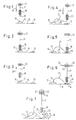
In der anliegenden Zeichnung sind mit der Bezugsziffer 10
eine Bond-Kapillare, 11 ein Gold-Bonddraht mit einem Mini-Ball
12 am unteren freien Drahtende, 13 eine am Bonddraht
11 angreifende Drahtklammer, 14 ein Bauelement mit einer
ersten Bondstelle 17, 15 ein lead-frame, 16 eine zweite
Bondstelle auf dem Lead-frame bzw. Substrat, und 18 eine
Abflammlanze gekennzeichnet.In the accompanying drawing, reference number 10
a bond capillary, 11 a gold bond wire with a
Ausgehend von einer hochgefahrenen Ausgangsposition eines
im einzelnen nicht näher dargestellten Bondkopfes wird der
Bondkopf samt Bond-Kapillare 10 mit abgeflammter Bonddraht-Kugel
bzw. Ball 12 auf eine erste Bondstelle 17 auf einem
Bauelement 14 abgesenkt, entsprechend Pfeil 19 in Fig. 1.
Die Absenkung der Bond-Kapillare 10 erfolgt unter Mitnahme
des Balls 12 und damit entsprechender Mitnahme des Bonddrahtes
11. Anschließend erfolgt das Aufschweißen des Balls
12 an der ersten Bondstelle 17 auf dem Bauelement 14 unter
Wärmezugabe definiertem Anpreßdruck und/oder Ultraschallunterstützung.Starting from a raised starting position of a
the bonding head, not shown in detail, is the
Bond head including bond capillary 10 with flamed bond wire ball
or
Dann wird der Bondkopf bzw. die Bond-Kapillare 10 wieder
hochgefahren (siehe Pfeil 20 in Fig. 3) und in eine vorgegebene
Loop-Position entsprechend Fig. 4 bewegt, unter Ausbildung
einer sogenannten Bonddraht-Schleife 21. In der
Loop-Position befindet sich die Bond-Kapillare oberhalb der
zweiten Bondstelle 16. Die Bond-Kapillare wird dann unter
entsprechender Mitnahme des Bonddrahtes 11 aus der
Loop-Position erneut abgesenkt (siehe Pfeil 22 in Fig. 4).
In abgesenkter Stellung entsprechend Fig. 5 erfolgt dann
das Aufschweißen des Bonddrahtes 11 an der zweiten Bondstelle
16 ebenfalls unter Wärmezugabe, definiertem Anpreßdruck
und/oder Ultraschallunterstützung.Then the bond head or the bond capillary 10 again
started up (see
Dann wird der Bondkopf bzw. die Bond-Kapillare 10 in
tail-length-Position 28 gefahren entsprechend Fig. 6. Anschließend
wird die Drahtklammer 13 aktiviert und entsprechend
den Pfeilen 23 in Fig. 6 in Drahtklemmstellung gebracht.
Dann wird zwischen der Drahtklammer und der zweiten
Bondstelle 16 eine elektrische Spannung angelegt, gegebenenfalls
über den lead-frame 15. Sobald diese Spannung anliegt
wird die Drahtklammer 13 entsprechend den Pfeilen 24
in Fig.7 nach oben bewegt bzw. hochgefahren unter entsprechender
Ausübung eines Zuges auf den Bonddraht 11, bis dieser
abreißt. Mit dem Abriß des Bonddrahtes 11 wird die
elektrische Verbindung zwischen Drahtklammer 13 und zweiter
Bondstelle 16 unterbrochen. Die Zug- bzw. Abreißbewegung
der Drahtklammer 13 wird gestoppt. Gleichzeitig wird die
Wegstrecke festgehalten, die die Drahtklammer 13 in Richtung
der Pfeile 24 bis zum Abriß des Bonddrahtes 11 zurückgelegt
hat.Then the bond head or the bond capillary 10 in
Tail-
Nach dem Abriß des Bonddrahtes 11 wird die hochgefahrene
Bond-Kapillare 10 wieder abgesenkt, bis die freie Drahtspitze
die mittlerweile in Abflammstellung gebrachte bzw.
eingeschwenkte Abflammlanze oder einen entsprechenden Anschlag
kontaktiert. Dann braucht der Bondkopf nur noch so
weit angehoben zu werden, bis ein vorbestimmter Abstand
zwischen der freien Drahtspitze und der Abflammlanze 18 erreicht
ist. Auf diese Weise läßt sich die Ball-Größe
dauerhaft exakt bestimmen. Die Abflammlanze 18 führt bei
dem Verfahren lediglich eine Bewegung in Richtung des Doppelpfeiles
29 in Fig. 7 aus.After the
Auf diese Weise ist die tatsächliche tail-length 25 (Fig.
7) bzw. die exakte Position des freien Bonddrahtendes oberhalb
der zweiten Bondstelle 16 bestimmbar, so daß es möglich
ist, die Einrichtung zum Abflammen des freien Bonddrahtendes
unter Ausbildung eines neuen Balls 12, nämlich
die Abflammlanze 18, gegenüber dem freien Bonddrahtende
bzw. der Drahtspitze so zu positionieren (siehe Doppelpfeil
29 in Fig.7), daß die Abflammlanze 18 stets einen vorbestimmten
Abstand zur Bonddrahtspitze aufweist. Dann wird
die Abflammlanze 18 aktiviert (Abflammfunke 27), so daß
sich der tail 25 zu einem neuen Ball 12 verformt.In this way the actual tail-length 25 (Fig.
7) or the exact position of the free bond wire end above
the
Anschließend wird die Drahtklammer 13 wieder geöffnet und
in die Ausgangsposition gemäß Fig. 1 abgesenkt. Ein neuer
Bondvorgang der beschriebenen Art kann wieder beginnen.Then the
Als Antrieb für die Drahtklammer 13 dient vorzugsweise ein
Schrittmotor. Die von der Drahtklammer 13 zurückgelegte
Wegstrecke bis zum Abriß des Bonddrahtes 11 wird dementsprechend
in Schritten (clocks) festgehalten. Vorzugsweise
erfolgt die Auf- und Abbewegung der Abflammlanze 18 in
Richtung des Doppelpfeiles 26 ebenfalls mittels eines
Schrittmotors, wobei die Zählwerke der beiden Schrittmotoren
über eine Rechnereinheit miteinander gekoppelt sind, so
daß die gewünschte Zuordnung der Abflammlanze 18 zur freien
Drahtspitze selbsttätig bzw. vollautomatisch herstellbar
ist.A preferably serves as a drive for the
Sobald sich die Drahtklammer 13 wieder in ihrer Startposition
gemäß Fig. 1 befindet, wird das der Drahtklammer 13
zugeordnete Zählwerk wieder auf Null gestellt. Auch die Abflammlanze
18 wird nach dem Abflammen des tails 25 wieder
in eine Nullposition gebracht. Sobald diese erreicht ist,
wird das dem Antrieb der Abflammlanze 18 zugeordnete Zählwerk
ebenfalls auf Null gestellt. Sowohl die Drahtklammer
13 als auch die Abflammlanze 18 befinden sich somit jeweils
in Ausgangs- bzw. Startposition, von der aus die gegenseitige
Positionierung von freier Drahtspitze und Abflammlanze
18 bestimmt und gesteuert wird.As soon as the
Durch das beschriebene Verfahren ist es möglich, die eingangs genannten Erscheinungen bzw. Größen, wie Drahtdehnung und Drahtverformung (seitliche Ausbiegung im unbelasteten Zustand), als Fehlgrößen zur exakten Ball-Dimensionierung auszuschließen.With the described method it is possible to start with mentioned phenomena or sizes, such as wire elongation and wire deformation (lateral deflection in the unloaded Condition), as defective sizes for exact ball dimensioning to exclude.
Als Kontaktsensor kann bei dem Verfahren ein herkömmlicher elektrischer (berührungsfreier), mechanischer oder Ultraschall-Sensor dienen.A conventional contact sensor can be used in the method electrical (non-contact), mechanical or ultrasonic sensor to serve.
Bei dem Verfahren läßt sich auch feststellen, ob überhaupt
ein ausreichend langer tail 25 vorhanden ist. Sofern nämlich
nach vorbestimmter Absenkung des Bondkopfes noch immer
kein Kontakt zur Abflammlanze 18 hergestellt ist, bedeutet
dies, daß die tail-length zu kurz ist, um einen ausreichend
großen Ball 12 ausbilden zu können.The process can also determine whether at all
a sufficiently
Claims (5)
- Ball bonding method, such as a gold-wire bonding method, which comprises the following process steps:characterized in thata) Positioning and lowering of a bonding capillary (10) having a singed bonding wire sphere (ball 12) on the lower, free end of a bonding wire (11) from a raised original position to a first bonding point (17);b) Welding on the ball (12) while supplying heat, with a defined contact pressure and/or with ultrasound assistance;c) Raising the bonding capillary (10);d) Forming a bonding wire loop (21);e) Welding the bonding wire (11) to a second bonding point (16) while supplying heat, with a defined contact pressure and/or with ultrasound assistance;f) Raising the bonding capillary (10) to a predetermined tail-length position (28), tearing off the bonding wire (11) by exerting tension on it by means of a wire clip (13) which acts on the bonding wire (11), and subsequently raising the bonding capillary (10) to the original position; andg) Singeing the free bonding-wire end to form a new ball (12),h) Before singeing the free bonding-wire end, a singeing lance (18), which is provided as a device for singeing the free bonding-wire end, is moved or pivoted into the singeing position;i) The bonding capillary (10) is then lowered until the free bonding-wire end or the wire tip makes contact with the singeing lance (18) or a movement-limiting element associated with it; andj) The bonding capillary (10) is then raised again through a predetermined distance until the free bonding-wire end is at a predetermined distance from the singeing lance (18).
- Method according to Claim 1,
characterized in that
the contact with the free bonding-wire end is confirmed by means of an electrical, mechanical and/or ultrasound sensor. - Apparatus for carrying out the method according to one of Claims 1 or 2, comprising a bonding capillary (10) having a bonding wire (11) which can be moved, respectively, towards and away from bonding points (16, 17), having a wire clip (13) which acts on the bonding wire (11) and, respectively, can be moved towards and away from the bonding points (16, 17), and having a device for applying an electrical voltage between the wire clip (13) and one bonding point (16),
characterized in that
the wire clip (13) which results in the bonding wire (11) being torn off is assigned a stepping drive which is coupled to a counting mechanism which determines the distance travelled by the wire clip (13) and can be set to zero in order once again to determine a further distance, and in that a contact sensor is provided in order to confirm a contact between the free bonding-wire end and the singeing lance (18) or a movement-limiting element associated with it. - Apparatus according to Claim 3,
characterized in that
a singeing lance (18) which is provided as a device for singeing the free bonding-wire end can be moved, respectively, towards and away from the bonding points (16, 17), the bonding lance (18) being assigned a stepping drive which is coupled to a counting mechanism which determines the distance travelled by the singeing lance (18) and can be set to zero in order once again to determine a further distance. - Apparatus according to Claim 3 or 4,
characterized in that
the contact sensor is designed as an electrical, mechanical or ultrasound sensor.
Applications Claiming Priority (3)
| Application Number | Priority Date | Filing Date | Title |
|---|---|---|---|
| DE19873703694 DE3703694A1 (en) | 1987-02-06 | 1987-02-06 | BALL BONDING METHOD AND DEVICE FOR CARRYING OUT THE SAME |
| DE3703694 | 1987-02-06 | ||
| EP87907960A EP0299987B1 (en) | 1987-02-06 | 1987-12-09 | Ball bonding process and device |
Related Parent Applications (2)
| Application Number | Title | Priority Date | Filing Date |
|---|---|---|---|
| EP87907960A Division EP0299987B1 (en) | 1987-02-06 | 1987-12-09 | Ball bonding process and device |
| EP87907960.6 Division | 1987-12-09 |
Publications (3)
| Publication Number | Publication Date |
|---|---|
| EP0533164A2 EP0533164A2 (en) | 1993-03-24 |
| EP0533164A3 EP0533164A3 (en) | 1993-07-14 |
| EP0533164B1 true EP0533164B1 (en) | 1999-03-31 |
Family
ID=6320422
Family Applications (2)
| Application Number | Title | Priority Date | Filing Date |
|---|---|---|---|
| EP87907960A Expired - Lifetime EP0299987B1 (en) | 1987-02-06 | 1987-12-09 | Ball bonding process and device |
| EP92115937A Expired - Lifetime EP0533164B1 (en) | 1987-02-06 | 1987-12-09 | Ball bonding method and apparatus for using the same |
Family Applications Before (1)
| Application Number | Title | Priority Date | Filing Date |
|---|---|---|---|
| EP87907960A Expired - Lifetime EP0299987B1 (en) | 1987-02-06 | 1987-12-09 | Ball bonding process and device |
Country Status (7)
| Country | Link |
|---|---|
| US (1) | US4925083A (en) |
| EP (2) | EP0299987B1 (en) |
| JP (1) | JPH01502066A (en) |
| KR (1) | KR960005549B1 (en) |
| AT (2) | ATE106607T1 (en) |
| DE (3) | DE3703694A1 (en) |
| WO (1) | WO1988005960A1 (en) |
Families Citing this family (94)
| Publication number | Priority date | Publication date | Assignee | Title |
|---|---|---|---|---|
| US5285949A (en) * | 1987-01-26 | 1994-02-15 | Hitachi, Ltd. | Wire-bonding method, wire-bonding apparatus, and semiconductor device produced by the wire-bonding method |
| US5014111A (en) * | 1987-12-08 | 1991-05-07 | Matsushita Electric Industrial Co., Ltd. | Electrical contact bump and a package provided with the same |
| US5326015A (en) * | 1993-03-29 | 1994-07-05 | Kulicke And Soffa Investments, Inc. | Wire bonder tail length monitor |
| DE4335468A1 (en) * | 1993-10-18 | 1995-04-20 | F&K Delvotec Bondtechnik Gmbh | Device and method for wire bonding |
| US5683255A (en) * | 1993-12-03 | 1997-11-04 | Menze; Marion John | Radio frequency connector assembly |
| US5868300A (en) * | 1995-06-29 | 1999-02-09 | Orthodyne Electronics Corporation | Articulated wire bonder |
| US5874354A (en) * | 1995-09-26 | 1999-02-23 | Siemens Aktiengesellschaft | Method for electrically connecting a semiconductor chip to at least one contact surface and smart card module and smart card produced by the method |
| DE29608277U1 (en) * | 1996-04-30 | 1996-09-19 | F&K Delvotec Bondtechnik Gmbh | Ball bonding device |
| US6098868A (en) * | 1997-05-23 | 2000-08-08 | Masushita Electric Industrial Co., Ltd. | Bump forming method and bump bonder |
| DE19812706A1 (en) * | 1998-03-23 | 1999-10-07 | F&K Delvotec Bondtechnik Gmbh | Method and device for "ball-bonding" |
| JP2001189340A (en) * | 1999-12-28 | 2001-07-10 | Shinkawa Ltd | Wire-bonding method and device thereof |
| DE10035175C1 (en) * | 2000-07-19 | 2002-01-03 | Fraunhofer Ges Forschung | Making electrical/mechanical connection between flexible thin film substrates involves positioning substrates so openings coincide, positioning bonding elements, pressing together |
| US6350632B1 (en) | 2000-09-20 | 2002-02-26 | Charles W. C. Lin | Semiconductor chip assembly with ball bond connection joint |
| US6511865B1 (en) | 2000-09-20 | 2003-01-28 | Charles W. C. Lin | Method for forming a ball bond connection joint on a conductive trace and conductive pad in a semiconductor chip assembly |
| US6350386B1 (en) | 2000-09-20 | 2002-02-26 | Charles W. C. Lin | Method of making a support circuit with a tapered through-hole for a semiconductor chip assembly |
| US6448108B1 (en) | 2000-10-02 | 2002-09-10 | Charles W. C. Lin | Method of making a semiconductor chip assembly with a conductive trace subtractively formed before and after chip attachment |
| US6544813B1 (en) | 2000-10-02 | 2003-04-08 | Charles W. C. Lin | Method of making a semiconductor chip assembly with a conductive trace subtractively formed before and after chip attachment |
| US6699780B1 (en) | 2000-10-13 | 2004-03-02 | Bridge Semiconductor Corporation | Method of connecting a conductive trace to a semiconductor chip using plasma undercut etching |
| US7129113B1 (en) | 2000-10-13 | 2006-10-31 | Bridge Semiconductor Corporation | Method of making a three-dimensional stacked semiconductor package with a metal pillar in an encapsulant aperture |
| US6872591B1 (en) | 2000-10-13 | 2005-03-29 | Bridge Semiconductor Corporation | Method of making a semiconductor chip assembly with a conductive trace and a substrate |
| US7132741B1 (en) | 2000-10-13 | 2006-11-07 | Bridge Semiconductor Corporation | Semiconductor chip assembly with carved bumped terminal |
| US7129575B1 (en) | 2000-10-13 | 2006-10-31 | Bridge Semiconductor Corporation | Semiconductor chip assembly with bumped metal pillar |
| US6576493B1 (en) | 2000-10-13 | 2003-06-10 | Bridge Semiconductor Corporation | Method of connecting a conductive trace and an insulative base to a semiconductor chip using multiple etch steps |
| US7075186B1 (en) | 2000-10-13 | 2006-07-11 | Bridge Semiconductor Corporation | Semiconductor chip assembly with interlocked contact terminal |
| US7262082B1 (en) | 2000-10-13 | 2007-08-28 | Bridge Semiconductor Corporation | Method of making a three-dimensional stacked semiconductor package with a metal pillar and a conductive interconnect in an encapsulant aperture |
| US7094676B1 (en) | 2000-10-13 | 2006-08-22 | Bridge Semiconductor Corporation | Semiconductor chip assembly with embedded metal pillar |
| US7264991B1 (en) | 2000-10-13 | 2007-09-04 | Bridge Semiconductor Corporation | Method of connecting a conductive trace to a semiconductor chip using conductive adhesive |
| US6667229B1 (en) | 2000-10-13 | 2003-12-23 | Bridge Semiconductor Corporation | Method of connecting a bumped compliant conductive trace and an insulative base to a semiconductor chip |
| US6673710B1 (en) | 2000-10-13 | 2004-01-06 | Bridge Semiconductor Corporation | Method of connecting a conductive trace and an insulative base to a semiconductor chip |
| US6537851B1 (en) | 2000-10-13 | 2003-03-25 | Bridge Semiconductor Corporation | Method of connecting a bumped compliant conductive trace to a semiconductor chip |
| US6492252B1 (en) | 2000-10-13 | 2002-12-10 | Bridge Semiconductor Corporation | Method of connecting a bumped conductive trace to a semiconductor chip |
| US6984576B1 (en) | 2000-10-13 | 2006-01-10 | Bridge Semiconductor Corporation | Method of connecting an additively and subtractively formed conductive trace and an insulative base to a semiconductor chip |
| US6740576B1 (en) | 2000-10-13 | 2004-05-25 | Bridge Semiconductor Corporation | Method of making a contact terminal with a plated metal peripheral sidewall portion for a semiconductor chip assembly |
| US6548393B1 (en) | 2000-10-13 | 2003-04-15 | Charles W. C. Lin | Semiconductor chip assembly with hardened connection joint |
| US6576539B1 (en) | 2000-10-13 | 2003-06-10 | Charles W.C. Lin | Semiconductor chip assembly with interlocked conductive trace |
| US6949408B1 (en) | 2000-10-13 | 2005-09-27 | Bridge Semiconductor Corporation | Method of connecting a conductive trace and an insulative base to a semiconductor chip using multiple etch steps |
| US6876072B1 (en) | 2000-10-13 | 2005-04-05 | Bridge Semiconductor Corporation | Semiconductor chip assembly with chip in substrate cavity |
| US7414319B2 (en) * | 2000-10-13 | 2008-08-19 | Bridge Semiconductor Corporation | Semiconductor chip assembly with metal containment wall and solder terminal |
| US7071089B1 (en) | 2000-10-13 | 2006-07-04 | Bridge Semiconductor Corporation | Method of making a semiconductor chip assembly with a carved bumped terminal |
| US7319265B1 (en) | 2000-10-13 | 2008-01-15 | Bridge Semiconductor Corporation | Semiconductor chip assembly with precision-formed metal pillar |
| US6908788B1 (en) | 2000-10-13 | 2005-06-21 | Bridge Semiconductor Corporation | Method of connecting a conductive trace to a semiconductor chip using a metal base |
| US7190080B1 (en) | 2000-10-13 | 2007-03-13 | Bridge Semiconductor Corporation | Semiconductor chip assembly with embedded metal pillar |
| US7009297B1 (en) | 2000-10-13 | 2006-03-07 | Bridge Semiconductor Corporation | Semiconductor chip assembly with embedded metal particle |
| US6440835B1 (en) | 2000-10-13 | 2002-08-27 | Charles W. C. Lin | Method of connecting a conductive trace to a semiconductor chip |
| US6444489B1 (en) | 2000-12-15 | 2002-09-03 | Charles W. C. Lin | Semiconductor chip assembly with bumped molded substrate |
| US6653170B1 (en) | 2001-02-06 | 2003-11-25 | Charles W. C. Lin | Semiconductor chip assembly with elongated wire ball bonded to chip and electrolessly plated to support circuit |
| US7993983B1 (en) | 2003-11-17 | 2011-08-09 | Bridge Semiconductor Corporation | Method of making a semiconductor chip assembly with chip and encapsulant grinding |
| US7538415B1 (en) | 2003-11-20 | 2009-05-26 | Bridge Semiconductor Corporation | Semiconductor chip assembly with bumped terminal, filler and insulative base |
| US7425759B1 (en) | 2003-11-20 | 2008-09-16 | Bridge Semiconductor Corporation | Semiconductor chip assembly with bumped terminal and filler |
| US8525314B2 (en) | 2004-11-03 | 2013-09-03 | Tessera, Inc. | Stacked packaging improvements |
| US7750483B1 (en) | 2004-11-10 | 2010-07-06 | Bridge Semiconductor Corporation | Semiconductor chip assembly with welded metal pillar and enlarged plated contact terminal |
| US7268421B1 (en) | 2004-11-10 | 2007-09-11 | Bridge Semiconductor Corporation | Semiconductor chip assembly with welded metal pillar that includes enlarged ball bond |
| US7446419B1 (en) | 2004-11-10 | 2008-11-04 | Bridge Semiconductor Corporation | Semiconductor chip assembly with welded metal pillar of stacked metal balls |
| US8058101B2 (en) | 2005-12-23 | 2011-11-15 | Tessera, Inc. | Microelectronic packages and methods therefor |
| JP4679427B2 (en) * | 2006-04-24 | 2011-04-27 | 株式会社新川 | Tail wire cutting method and program for bonding apparatus |
| ATE472387T1 (en) | 2006-09-05 | 2010-07-15 | Univ Berlin Tech | METHOD AND DEVICE FOR CONTROLLING THE PRODUCTION OF WIRE BONDING CONNECTIONS |
| US7811863B1 (en) | 2006-10-26 | 2010-10-12 | Bridge Semiconductor Corporation | Method of making a semiconductor chip assembly with metal pillar and encapsulant grinding and heat sink attachment |
| US7494843B1 (en) | 2006-12-26 | 2009-02-24 | Bridge Semiconductor Corporation | Method of making a semiconductor chip assembly with thermal conductor and encapsulant grinding |
| US7896218B2 (en) | 2007-06-28 | 2011-03-01 | Western Digital Technologies, Inc. | Apparatus and method for conductive metal ball bonding with electrostatic discharge detection |
| US8020290B2 (en) * | 2009-06-14 | 2011-09-20 | Jayna Sheats | Processes for IC fabrication |
| US8482111B2 (en) | 2010-07-19 | 2013-07-09 | Tessera, Inc. | Stackable molded microelectronic packages |
| KR101128063B1 (en) | 2011-05-03 | 2012-04-23 | 테세라, 인코포레이티드 | Package-on-package assembly with wire bonds to encapsulation surface |
| US8404520B1 (en) | 2011-10-17 | 2013-03-26 | Invensas Corporation | Package-on-package assembly with wire bond vias |
| US8946757B2 (en) | 2012-02-17 | 2015-02-03 | Invensas Corporation | Heat spreading substrate with embedded interconnects |
| US8372741B1 (en) | 2012-02-24 | 2013-02-12 | Invensas Corporation | Method for package-on-package assembly with wire bonds to encapsulation surface |
| US8835228B2 (en) | 2012-05-22 | 2014-09-16 | Invensas Corporation | Substrate-less stackable package with wire-bond interconnect |
| US9391008B2 (en) | 2012-07-31 | 2016-07-12 | Invensas Corporation | Reconstituted wafer-level package DRAM |
| US9502390B2 (en) | 2012-08-03 | 2016-11-22 | Invensas Corporation | BVA interposer |
| US8878353B2 (en) | 2012-12-20 | 2014-11-04 | Invensas Corporation | Structure for microelectronic packaging with bond elements to encapsulation surface |
| US9136254B2 (en) | 2013-02-01 | 2015-09-15 | Invensas Corporation | Microelectronic package having wire bond vias and stiffening layer |
| TWI487046B (en) * | 2013-04-03 | 2015-06-01 | 矽品精密工業股份有限公司 | Method of welding a solder wire |
| TWI518816B (en) * | 2013-07-04 | 2016-01-21 | 先進科技新加坡有限公司 | Method and apparatus for measuring a free air ball size during wire bonding |
| US9167710B2 (en) | 2013-08-07 | 2015-10-20 | Invensas Corporation | Embedded packaging with preformed vias |
| US9685365B2 (en) * | 2013-08-08 | 2017-06-20 | Invensas Corporation | Method of forming a wire bond having a free end |
| US20150076714A1 (en) | 2013-09-16 | 2015-03-19 | Invensas Corporation | Microelectronic element with bond elements to encapsulation surface |
| US9379074B2 (en) | 2013-11-22 | 2016-06-28 | Invensas Corporation | Die stacks with one or more bond via arrays of wire bond wires and with one or more arrays of bump interconnects |
| US9583456B2 (en) | 2013-11-22 | 2017-02-28 | Invensas Corporation | Multiple bond via arrays of different wire heights on a same substrate |
| US9263394B2 (en) | 2013-11-22 | 2016-02-16 | Invensas Corporation | Multiple bond via arrays of different wire heights on a same substrate |
| US9583411B2 (en) | 2014-01-17 | 2017-02-28 | Invensas Corporation | Fine pitch BVA using reconstituted wafer with area array accessible for testing |
| US10381326B2 (en) | 2014-05-28 | 2019-08-13 | Invensas Corporation | Structure and method for integrated circuits packaging with increased density |
| US9735084B2 (en) | 2014-12-11 | 2017-08-15 | Invensas Corporation | Bond via array for thermal conductivity |
| US9888579B2 (en) | 2015-03-05 | 2018-02-06 | Invensas Corporation | Pressing of wire bond wire tips to provide bent-over tips |
| US9502372B1 (en) | 2015-04-30 | 2016-11-22 | Invensas Corporation | Wafer-level packaging using wire bond wires in place of a redistribution layer |
| US9761554B2 (en) | 2015-05-07 | 2017-09-12 | Invensas Corporation | Ball bonding metal wire bond wires to metal pads |
| US9881895B2 (en) * | 2015-08-18 | 2018-01-30 | Lockheed Martin Corporation | Wire bonding methods and systems incorporating metal nanoparticles |
| US9490222B1 (en) | 2015-10-12 | 2016-11-08 | Invensas Corporation | Wire bond wires for interference shielding |
| US10490528B2 (en) | 2015-10-12 | 2019-11-26 | Invensas Corporation | Embedded wire bond wires |
| US10332854B2 (en) | 2015-10-23 | 2019-06-25 | Invensas Corporation | Anchoring structure of fine pitch bva |
| US10181457B2 (en) | 2015-10-26 | 2019-01-15 | Invensas Corporation | Microelectronic package for wafer-level chip scale packaging with fan-out |
| US10043779B2 (en) | 2015-11-17 | 2018-08-07 | Invensas Corporation | Packaged microelectronic device for a package-on-package device |
| US9659848B1 (en) | 2015-11-18 | 2017-05-23 | Invensas Corporation | Stiffened wires for offset BVA |
| US9984992B2 (en) | 2015-12-30 | 2018-05-29 | Invensas Corporation | Embedded wire bond wires for vertical integration with separate surface mount and wire bond mounting surfaces |
| US9935075B2 (en) | 2016-07-29 | 2018-04-03 | Invensas Corporation | Wire bonding method and apparatus for electromagnetic interference shielding |
| US10299368B2 (en) | 2016-12-21 | 2019-05-21 | Invensas Corporation | Surface integrated waveguides and circuit structures therefor |
Family Cites Families (12)
| Publication number | Priority date | Publication date | Assignee | Title |
|---|---|---|---|---|
| US3767101A (en) * | 1972-01-26 | 1973-10-23 | Hughes Aircraft Co | Pulse vibrator for thermocompression bonding |
| US3863827A (en) * | 1972-11-10 | 1975-02-04 | Mech El Ind Inc | Tailless wire bonder |
| US3941486A (en) * | 1974-06-03 | 1976-03-02 | The Computervision Corporation | Wire bonder |
| US3934108A (en) * | 1974-09-16 | 1976-01-20 | Uthe Technology, Inc. | Lead bonding method and apparatus |
| GB1468974A (en) * | 1975-05-23 | 1977-03-30 | Ferranti Ltd | Manufacture of semiconductor devices |
| US4109846A (en) * | 1977-05-17 | 1978-08-29 | Sola Basic Industries, Inc. | Automatic height sensor for semiconductor bonding tool, wafer probe or the like |
| US4213556A (en) * | 1978-10-02 | 1980-07-22 | General Motors Corporation | Method and apparatus to detect automatic wire bonder failure |
| US4266710A (en) * | 1978-11-22 | 1981-05-12 | Kulicke And Soffa Industries Inc. | Wire bonding apparatus |
| DE3037735A1 (en) * | 1980-10-06 | 1982-05-13 | TS-Electronic Vertriebs-GmbH, 8000 München | Semiconductor component surface contacting system - uses thin aluminium wire and spark discharge cover precisely adjustable spark gap and stable protection gas flow during melting |
| JPS57211240A (en) * | 1981-06-22 | 1982-12-25 | Hitachi Ltd | Wire bonder |
| US4555052A (en) * | 1983-02-28 | 1985-11-26 | Fairchild Camera & Instrument Corporation | Lead wire bond attempt detection |
| US4586642A (en) * | 1985-05-13 | 1986-05-06 | Kulicke And Soffa Industries Inc. | Wire bond monitoring system |
-
1987
- 1987-02-06 DE DE19873703694 patent/DE3703694A1/en not_active Withdrawn
- 1987-12-09 AT AT87907960T patent/ATE106607T1/en not_active IP Right Cessation
- 1987-12-09 EP EP87907960A patent/EP0299987B1/en not_active Expired - Lifetime
- 1987-12-09 DE DE3789962T patent/DE3789962D1/en not_active Expired - Fee Related
- 1987-12-09 EP EP92115937A patent/EP0533164B1/en not_active Expired - Lifetime
- 1987-12-09 JP JP63500228A patent/JPH01502066A/en active Pending
- 1987-12-09 US US07/272,780 patent/US4925083A/en not_active Expired - Lifetime
- 1987-12-09 DE DE3752266T patent/DE3752266D1/en not_active Expired - Lifetime
- 1987-12-09 KR KR1019880701243A patent/KR960005549B1/en active IP Right Grant
- 1987-12-09 WO PCT/EP1987/000765 patent/WO1988005960A1/en active IP Right Grant
- 1987-12-09 AT AT92115937T patent/ATE178431T1/en not_active IP Right Cessation
Also Published As
| Publication number | Publication date |
|---|---|
| EP0533164A3 (en) | 1993-07-14 |
| WO1988005960A1 (en) | 1988-08-11 |
| EP0299987B1 (en) | 1994-06-01 |
| ATE106607T1 (en) | 1994-06-15 |
| DE3752266D1 (en) | 1999-05-06 |
| JPH01502066A (en) | 1989-07-13 |
| KR890700921A (en) | 1989-04-28 |
| EP0533164A2 (en) | 1993-03-24 |
| DE3789962D1 (en) | 1994-07-07 |
| US4925083A (en) | 1990-05-15 |
| EP0299987A1 (en) | 1989-01-25 |
| ATE178431T1 (en) | 1999-04-15 |
| KR960005549B1 (en) | 1996-04-26 |
| DE3703694A1 (en) | 1988-08-18 |
Similar Documents
| Publication | Publication Date | Title |
|---|---|---|
| EP0533164B1 (en) | Ball bonding method and apparatus for using the same | |
| DE19752319B4 (en) | An ultrasonic wire-bonding apparatus comprising a device for testing a bond connection and a method for testing a bond connection produced by means of an ultrasonic wire-bonding tool | |
| DE19747116B4 (en) | Method for establishing a connection between the conductor tracks of a flat cable and connections of a conductor block | |
| DE2608250A1 (en) | PROCEDURE FOR CONTACTING CONNECTOR CONTACTS ON SEMICONDUCTOR BODIES | |
| DE3810929C2 (en) | ||
| DE4205742A1 (en) | Holding tongs for winding EM core - have cooperating tong plates providing guidance for conductor wire wound onto core | |
| DE3333601A1 (en) | WIRE CONNECTION OR WIRING DEVICE | |
| DE2032302A1 (en) | Method and device for attaching leads to metallized Be range from semiconductor surfaces | |
| EP0656310B1 (en) | Method and apparatus for producing a laminate | |
| DE3933982C2 (en) | Contacting method and contacting device | |
| DE102012112667A1 (en) | Method and apparatus for forming a nail bump | |
| DE1514285C3 (en) | A method of manufacturing a semiconductor device | |
| CH682597A5 (en) | Kontaktierungsqualitäts analyzer. | |
| DE4129933C2 (en) | Method and device for wire bonding | |
| EP1474266A1 (en) | Arrangement for wire bonding and method for producing a bonding connection | |
| DE19625638A1 (en) | Vertically movable ultrasound bonding head apparatus for semiconductor chip connection | |
| DE3504422C2 (en) | ||
| DE102015017014B4 (en) | Anchor with windings and method for connecting winding ends of the armature to a terminal | |
| DE4307080A1 (en) | Method and device for the production of a coil arrangement | |
| DE1465095B2 (en) | METHOD AND DEVICE FOR ELECTRICALLY CONNECTING TWO CONNECTING PINS ON A CIRCUIT BOARD | |
| DE1591226A1 (en) | Device for forming and placing contact bridges on electrical circuits | |
| DE3739955A1 (en) | DEVICE FOR ULTRASONIC WIRE CONTACT | |
| DE1160110B (en) | Method and device for the automatic construction of semiconductor crystal diodes | |
| DE2343365A1 (en) | ELECTRIC WELDING MACHINE | |
| DE2522022C3 (en) | Method for applying a wire connection between a contact point on a semiconductor arrangement and a feed conductor |
Legal Events
| Date | Code | Title | Description |
|---|---|---|---|
| PUAI | Public reference made under article 153(3) epc to a published international application that has entered the european phase |
Free format text: ORIGINAL CODE: 0009012 |
|
| AC | Divisional application: reference to earlier application |
Ref document number: 299987 Country of ref document: EP |
|
| AK | Designated contracting states |
Kind code of ref document: A2 Designated state(s): AT BE CH DE FR GB IT LI NL SE |
|
| RIN1 | Information on inventor provided before grant (corrected) |
Inventor name: BIRGEL, WALTER Inventor name: FARASSAT, FARHAD |
|
| PUAL | Search report despatched |
Free format text: ORIGINAL CODE: 0009013 |
|
| AK | Designated contracting states |
Kind code of ref document: A3 Designated state(s): AT BE CH DE FR GB IT LI NL SE |
|
| 17P | Request for examination filed |
Effective date: 19940317 |
|
| 17Q | First examination report despatched |
Effective date: 19960619 |
|
| GRAG | Despatch of communication of intention to grant |
Free format text: ORIGINAL CODE: EPIDOS AGRA |
|
| GRAG | Despatch of communication of intention to grant |
Free format text: ORIGINAL CODE: EPIDOS AGRA |
|
| GRAH | Despatch of communication of intention to grant a patent |
Free format text: ORIGINAL CODE: EPIDOS IGRA |
|
| GRAH | Despatch of communication of intention to grant a patent |
Free format text: ORIGINAL CODE: EPIDOS IGRA |
|
| GRAA | (expected) grant |
Free format text: ORIGINAL CODE: 0009210 |
|
| RAP1 | Party data changed (applicant data changed or rights of an application transferred) |
Owner name: F & K DELVOTEC BONDTECHNIK GMBH |
|
| AC | Divisional application: reference to earlier application |
Ref document number: 299987 Country of ref document: EP |
|
| AK | Designated contracting states |
Kind code of ref document: B1 Designated state(s): AT BE CH DE FR GB IT LI NL SE |
|
| REF | Corresponds to: |
Ref document number: 178431 Country of ref document: AT Date of ref document: 19990415 Kind code of ref document: T |
|
| REG | Reference to a national code |
Ref country code: CH Ref legal event code: NV Representative=s name: RITSCHER & SEIFERT Ref country code: CH Ref legal event code: EP |
|
| REF | Corresponds to: |
Ref document number: 3752266 Country of ref document: DE Date of ref document: 19990506 |
|
| GBT | Gb: translation of ep patent filed (gb section 77(6)(a)/1977) |
Effective date: 19990610 |
|
| ET | Fr: translation filed | ||
| PLBE | No opposition filed within time limit |
Free format text: ORIGINAL CODE: 0009261 |
|
| STAA | Information on the status of an ep patent application or granted ep patent |
Free format text: STATUS: NO OPPOSITION FILED WITHIN TIME LIMIT |
|
| 26N | No opposition filed | ||
| REG | Reference to a national code |
Ref country code: GB Ref legal event code: IF02 |
|
| PGFP | Annual fee paid to national office [announced via postgrant information from national office to epo] |
Ref country code: GB Payment date: 20021118 Year of fee payment: 16 |
|
| PGFP | Annual fee paid to national office [announced via postgrant information from national office to epo] |
Ref country code: AT Payment date: 20021223 Year of fee payment: 16 |
|
| PGFP | Annual fee paid to national office [announced via postgrant information from national office to epo] |
Ref country code: SE Payment date: 20021227 Year of fee payment: 16 |
|
| PGFP | Annual fee paid to national office [announced via postgrant information from national office to epo] |
Ref country code: BE Payment date: 20030107 Year of fee payment: 16 |
|
| PG25 | Lapsed in a contracting state [announced via postgrant information from national office to epo] |
Ref country code: GB Free format text: LAPSE BECAUSE OF NON-PAYMENT OF DUE FEES Effective date: 20031209 Ref country code: AT Free format text: LAPSE BECAUSE OF NON-PAYMENT OF DUE FEES Effective date: 20031209 |
|
| PG25 | Lapsed in a contracting state [announced via postgrant information from national office to epo] |
Ref country code: SE Free format text: LAPSE BECAUSE OF NON-PAYMENT OF DUE FEES Effective date: 20031210 |
|
| PGFP | Annual fee paid to national office [announced via postgrant information from national office to epo] |
Ref country code: CH Payment date: 20031212 Year of fee payment: 17 |
|
| PGFP | Annual fee paid to national office [announced via postgrant information from national office to epo] |
Ref country code: NL Payment date: 20031217 Year of fee payment: 17 |
|
| PGFP | Annual fee paid to national office [announced via postgrant information from national office to epo] |
Ref country code: FR Payment date: 20031218 Year of fee payment: 17 |
|
| PG25 | Lapsed in a contracting state [announced via postgrant information from national office to epo] |
Ref country code: BE Free format text: LAPSE BECAUSE OF NON-PAYMENT OF DUE FEES Effective date: 20031231 |
|
| BERE | Be: lapsed |
Owner name: F & K *DELVOTEC BONDTECHNIK G.M.B.H. Effective date: 20031231 |
|
| GBPC | Gb: european patent ceased through non-payment of renewal fee |
Effective date: 20031209 |
|
| EUG | Se: european patent has lapsed | ||
| PG25 | Lapsed in a contracting state [announced via postgrant information from national office to epo] |
Ref country code: LI Free format text: LAPSE BECAUSE OF NON-PAYMENT OF DUE FEES Effective date: 20041231 Ref country code: CH Free format text: LAPSE BECAUSE OF NON-PAYMENT OF DUE FEES Effective date: 20041231 |
|
| PG25 | Lapsed in a contracting state [announced via postgrant information from national office to epo] |
Ref country code: NL Free format text: LAPSE BECAUSE OF NON-PAYMENT OF DUE FEES Effective date: 20050701 |
|
| REG | Reference to a national code |
Ref country code: CH Ref legal event code: PL |
|
| PG25 | Lapsed in a contracting state [announced via postgrant information from national office to epo] |
Ref country code: FR Free format text: LAPSE BECAUSE OF NON-PAYMENT OF DUE FEES Effective date: 20050831 |
|
| NLV4 | Nl: lapsed or anulled due to non-payment of the annual fee |
Effective date: 20050701 |
|
| REG | Reference to a national code |
Ref country code: FR Ref legal event code: ST |
|
| PG25 | Lapsed in a contracting state [announced via postgrant information from national office to epo] |
Ref country code: IT Free format text: LAPSE BECAUSE OF NON-PAYMENT OF DUE FEES;WARNING: LAPSES OF ITALIAN PATENTS WITH EFFECTIVE DATE BEFORE 2007 MAY HAVE OCCURRED AT ANY TIME BEFORE 2007. THE CORRECT EFFECTIVE DATE MAY BE DIFFERENT FROM THE ONE RECORDED. Effective date: 20051209 |
|
| PGFP | Annual fee paid to national office [announced via postgrant information from national office to epo] |
Ref country code: DE Payment date: 20070226 Year of fee payment: 20 |