EP0529953A1 - Placement and bonding technique - Google Patents
Placement and bonding technique Download PDFInfo
- Publication number
- EP0529953A1 EP0529953A1 EP92307623A EP92307623A EP0529953A1 EP 0529953 A1 EP0529953 A1 EP 0529953A1 EP 92307623 A EP92307623 A EP 92307623A EP 92307623 A EP92307623 A EP 92307623A EP 0529953 A1 EP0529953 A1 EP 0529953A1
- Authority
- EP
- European Patent Office
- Prior art keywords
- sidewalls
- vacuum
- bonding tool
- channel
- bonding
- Prior art date
- Legal status (The legal status is an assumption and is not a legal conclusion. Google has not performed a legal analysis and makes no representation as to the accuracy of the status listed.)
- Granted
Links
Images


Classifications
-
- G—PHYSICS
- G02—OPTICS
- G02B—OPTICAL ELEMENTS, SYSTEMS OR APPARATUS
- G02B6/00—Light guides; Structural details of arrangements comprising light guides and other optical elements, e.g. couplings
- G02B6/24—Coupling light guides
- G02B6/36—Mechanical coupling means
- G02B6/3616—Holders, macro size fixtures for mechanically holding or positioning fibres, e.g. on an optical bench
- G02B6/362—Vacuum holders for optical elements
-
- B—PERFORMING OPERATIONS; TRANSPORTING
- B23—MACHINE TOOLS; METAL-WORKING NOT OTHERWISE PROVIDED FOR
- B23K—SOLDERING OR UNSOLDERING; WELDING; CLADDING OR PLATING BY SOLDERING OR WELDING; CUTTING BY APPLYING HEAT LOCALLY, e.g. FLAME CUTTING; WORKING BY LASER BEAM
- B23K20/00—Non-electric welding by applying impact or other pressure, with or without the application of heat, e.g. cladding or plating
- B23K20/02—Non-electric welding by applying impact or other pressure, with or without the application of heat, e.g. cladding or plating by means of a press ; Diffusion bonding
-
- B—PERFORMING OPERATIONS; TRANSPORTING
- B23—MACHINE TOOLS; METAL-WORKING NOT OTHERWISE PROVIDED FOR
- B23K—SOLDERING OR UNSOLDERING; WELDING; CLADDING OR PLATING BY SOLDERING OR WELDING; CUTTING BY APPLYING HEAT LOCALLY, e.g. FLAME CUTTING; WORKING BY LASER BEAM
- B23K33/00—Specially-profiled edge portions of workpieces for making soldering or welding connections; Filling the seams formed thereby
-
- G—PHYSICS
- G02—OPTICS
- G02B—OPTICAL ELEMENTS, SYSTEMS OR APPARATUS
- G02B6/00—Light guides; Structural details of arrangements comprising light guides and other optical elements, e.g. couplings
- G02B6/24—Coupling light guides
- G02B6/26—Optical coupling means
- G02B6/32—Optical coupling means having lens focusing means positioned between opposed fibre ends
-
- G—PHYSICS
- G02—OPTICS
- G02B—OPTICAL ELEMENTS, SYSTEMS OR APPARATUS
- G02B6/00—Light guides; Structural details of arrangements comprising light guides and other optical elements, e.g. couplings
- G02B6/24—Coupling light guides
- G02B6/36—Mechanical coupling means
- G02B6/3628—Mechanical coupling means for mounting fibres to supporting carriers
- G02B6/3632—Mechanical coupling means for mounting fibres to supporting carriers characterised by the cross-sectional shape of the mechanical coupling means
- G02B6/3636—Mechanical coupling means for mounting fibres to supporting carriers characterised by the cross-sectional shape of the mechanical coupling means the mechanical coupling means being grooves
-
- G—PHYSICS
- G02—OPTICS
- G02B—OPTICAL ELEMENTS, SYSTEMS OR APPARATUS
- G02B6/00—Light guides; Structural details of arrangements comprising light guides and other optical elements, e.g. couplings
- G02B6/24—Coupling light guides
- G02B6/42—Coupling light guides with opto-electronic elements
- G02B6/4201—Packages, e.g. shape, construction, internal or external details
- G02B6/4219—Mechanical fixtures for holding or positioning the elements relative to each other in the couplings; Alignment methods for the elements, e.g. measuring or observing methods especially used therefor
- G02B6/422—Active alignment, i.e. moving the elements in response to the detected degree of coupling or position of the elements
- G02B6/4226—Positioning means for moving the elements into alignment, e.g. alignment screws, deformation of the mount
-
- G—PHYSICS
- G02—OPTICS
- G02B—OPTICAL ELEMENTS, SYSTEMS OR APPARATUS
- G02B6/00—Light guides; Structural details of arrangements comprising light guides and other optical elements, e.g. couplings
- G02B6/24—Coupling light guides
- G02B6/42—Coupling light guides with opto-electronic elements
- G02B6/4201—Packages, e.g. shape, construction, internal or external details
- G02B6/4219—Mechanical fixtures for holding or positioning the elements relative to each other in the couplings; Alignment methods for the elements, e.g. measuring or observing methods especially used therefor
- G02B6/4236—Fixing or mounting methods of the aligned elements
-
- G—PHYSICS
- G02—OPTICS
- G02B—OPTICAL ELEMENTS, SYSTEMS OR APPARATUS
- G02B7/00—Mountings, adjusting means, or light-tight connections, for optical elements
- G02B7/02—Mountings, adjusting means, or light-tight connections, for optical elements for lenses
- G02B7/027—Mountings, adjusting means, or light-tight connections, for optical elements for lenses the lens being in the form of a sphere or ball
-
- Y—GENERAL TAGGING OF NEW TECHNOLOGICAL DEVELOPMENTS; GENERAL TAGGING OF CROSS-SECTIONAL TECHNOLOGIES SPANNING OVER SEVERAL SECTIONS OF THE IPC; TECHNICAL SUBJECTS COVERED BY FORMER USPC CROSS-REFERENCE ART COLLECTIONS [XRACs] AND DIGESTS
- Y10—TECHNICAL SUBJECTS COVERED BY FORMER USPC
- Y10S—TECHNICAL SUBJECTS COVERED BY FORMER USPC CROSS-REFERENCE ART COLLECTIONS [XRACs] AND DIGESTS
- Y10S269/00—Work holders
- Y10S269/903—Work holder for electrical circuit assemblages or wiring systems
-
- Y—GENERAL TAGGING OF NEW TECHNOLOGICAL DEVELOPMENTS; GENERAL TAGGING OF CROSS-SECTIONAL TECHNOLOGIES SPANNING OVER SEVERAL SECTIONS OF THE IPC; TECHNICAL SUBJECTS COVERED BY FORMER USPC CROSS-REFERENCE ART COLLECTIONS [XRACs] AND DIGESTS
- Y10—TECHNICAL SUBJECTS COVERED BY FORMER USPC
- Y10T—TECHNICAL SUBJECTS COVERED BY FORMER US CLASSIFICATION
- Y10T279/00—Chucks or sockets
- Y10T279/11—Vacuum
Definitions
- This invention relates to placement and bonding techniques and, more particularly, to methods and apparatus for bonding elements such as glass spheres and optical fibers to substrates.
- Optical systems typically require a number of photonics modules for operating on lightwaves and coupling light to and from optoelectronic devices such as lasers, light emitting diodes, and photodetectors.
- the fundamental components of such photonics modules include optical fibers for transmitting light and spherical lenses for efficiently coupling light to and from optoelectronic devices and optical fibers.
- Silicon is a favored material for the construction of photonics modules because of the precision with which support walls can be formed in silicon for supporting and aligning the various optoelectronic devices, spherical or ball lenses, and optical fibers.
- aluminum can be coated on the silicon surface and that one can avoid the need for epoxies or other adhesives by using heat and pressure to bond the glass elements to the aluminum.
- the invention comprises a tool that can be robotically operated to pick up an optical element such as a ball lens or an optical fiber, place it in a groove or depression of a substrate, and apply pressure to it so that it is bonded to the substrate.
- the tool comprises a retracting element holder surrounding a bonding tool.
- a vacuum channel communicates with the element holder so that, by the application of a vacuum, it can pick up an optical element.
- the tool then moves the element to place it, for example, in a depression of a substrate, whereupon the vacuum is released, thereby to allow the element to nest between opposing sidewalls of the depression.
- the retracting element holder is simultaneously retracted vertically upwardly to expose a bonding surface of the bonding tool. After the element has nested in the groove, the bonding tool contacts the element and forces it against opposite sidewalls of the depression to bond the optical element to the sidewalls.
- An advantage of the invention is that a single tool functions both to place the optical element in the groove and to make the thermo-compression bond, which shortens the manufacturing cycle with respect to systems which would require separate cycles and separate tools for accomplishing these functions.
- the step of allowing the element to nest in the depression permits a natural alignment of the optical element within the depression and causes applied forces to be distributed symmetrically during the bonding step.
- FIG. 1 there is shown schematically a placement and bonding apparatus 11 for picking up a curved optical element, illustratively a ball lens 12, placing it at a proper location such as in a depression 13 of a silicon substrate 14, and bonding it to the substrate in accordance with an illustrative embodiment of the invention.
- the depression 13 is illustratively made by etching into a properly mounted crystalline silicon substrate to make a pyramid-shaped depression, a top view of which is shown in FIG. 2.
- the sidewalls can be very precisely located using known techniques of masking and etching and may be coated with a thin layer 15 of aluminum.
- the apparatus 11 comprises a bonding tool 16 which is surrounded by a retracting element holder 17.
- a vacuum channel 18 in the bonding tool communicates with a vacuum source 19 to apply a partial vacuum in a gap 20 between the bonding tool 16 and the element holder 17.
- a solenoid winding 22 surrounds a portion of the placement and bonding tool 11 which, when activated, causes a retraction of the element holder 17 to a higher vertical location within the apparatus 11, as shown in FIG. 3.
- the apparatus 11 is preferably part of a robotic apparatus controlled by a computer 23. It is moveable in X, Y and vertical directions by a motor or motors shown schematically at 24, controlled by the computer 23. In operation, apparatus 11 would normally be moved first to a tray of ball lenses. Tool 17 contacts a ball lens, with the vacuum activated by the computer 23 through a valve 25, to cause the ball lens 12 to adhere to the element holder 17. The apparatus 11 then is moved to a location over the depression 13 of the substrate 14, as shown in FIG. 1.
- the ball lens 12 may typically be three hundred microns in diameter, and it is therefore difficult to center the ball lens exactly at the apex of the pyramidal depression 13, required for thermo-compression bonding of the ball lens to the substrate. Therefore, in accordance with the invention, after rough placement, as shown in FIG. 1, which may not be precisely centered with respect to the depression 13, the vacuum is released by operation of the valve 25, whereupon the ball lens 12 is allowed to drop by gravity into the depression 13.
- the computer actuates solenoid 22 to retract holder 17 in a vertical upward direction, as shown. This retracting allows a lower horizontal surface of the bonding tool 16 to make contact with the ball lens 12. Thereafter, the computer actuates motor 24 to cause the apparatus 11 to move vertically downwardly.
- thermo-compression bonding of glass to aluminum simply requires the simultaneous application of heat and pressure.
- the substrate 14 may be heated by a heater schematically shown at 10, while pressure on the ball is provided by the bonding tool 16 exerting a downward force on the ball lens 12.
- the applied force may be six hundred grams, and the heat applied may be sufficient to raise the temperature of the substrate 14 to three hundred fifty degrees Centigrade.
- the pressure may be applied for three seconds to effect the thermo-compression bond.
- the computer 23 causes the apparatus 11 to rise from the ball lens 12 and to commence another cycle of operation.
- the bonding tool 16 should have a sufficient area to insure contact with the centered ball lens. That is, if the positioning accuracy of the tool is, say, five microns, the length and width of the lower surface of bonding tool 16 should be at least ten microns to insure contact of the bonding tool to the ball lens after centering. As can be appreciated from FIG. 2, the bonding tool applies force that is equally distributed to three opposing sidewalls 15.
- the substrate 14 may contain intersecting V-grooves (not shown) for the purpose of defining the position of ball lens 12.
- the element 12 may constitute an optical fiber 12′ which is mounted in a V-groove 13′.
- surfaces 28 (FIG. 3) of holder element 17 were flat and could accommodate both spherical glass balls and cylindrical optical fibers.
- the surfaces 28 could be made to match the surfaces only of a cylinder or only of a sphere if so desired.
- the apparatus 11 which was built and tested was operated as part of a Seiko XY3000 robot, commercially available from Seiko Instrument, Ltd., Torrance, California.
- acoustic energy can be used as an alternative to heat in the bonding step.
- the invention is also applicable to other methods of bonding using various solders and adhesives.
- epoxy adhesive for example, downward pressure on the optical element is often required for centering the element, seating it, and redistributing the fluid epoxy.
- various solders requires a downward force to insure reliable seating and bonding.
- an embodiment using an adhesive is identical to the illustrative embodiment except that, prior to deposit of the ball lens, either the ball lens or the sidewalls are coated with a fluid adhesive and, after the operation, the adhesive is allowed to harden.
- solder is identical to the illustrative embodiment except that, prior to deposit of the ball lens, either the lens or the sidewalls are coated with solder which after deposit is heated to a fluid condition and, after the operation, is cooled and allowed to be hardened.
- solder which after deposit is heated to a fluid condition and, after the operation, is cooled and allowed to be hardened.
Landscapes
- Physics & Mathematics (AREA)
- General Physics & Mathematics (AREA)
- Optics & Photonics (AREA)
- Engineering & Computer Science (AREA)
- Mechanical Engineering (AREA)
- Optical Couplings Of Light Guides (AREA)
- Mounting And Adjusting Of Optical Elements (AREA)
Abstract
Description
- This invention relates to placement and bonding techniques and, more particularly, to methods and apparatus for bonding elements such as glass spheres and optical fibers to substrates.
- Optical systems typically require a number of photonics modules for operating on lightwaves and coupling light to and from optoelectronic devices such as lasers, light emitting diodes, and photodetectors. The fundamental components of such photonics modules include optical fibers for transmitting light and spherical lenses for efficiently coupling light to and from optoelectronic devices and optical fibers. Silicon is a favored material for the construction of photonics modules because of the precision with which support walls can be formed in silicon for supporting and aligning the various optoelectronic devices, spherical or ball lenses, and optical fibers.
- It can be shown that aluminum can be coated on the silicon surface and that one can avoid the need for epoxies or other adhesives by using heat and pressure to bond the glass elements to the aluminum.
- In the commercial production of apparatus such as photonics modules, it would be desirable to use machines for placing and bonding optical elements to the substrate. Since such elements must be located with precision, it has been difficult to provide robotic apparatus which is capable of placing elements with the required precision and also applying the pressure to them needed for thermocompression. Separate placement and bonding, of course, increases the expense of the process, and it would be desirable to provide equipment capable of placing and bonding optical elements to a substrate in a single step.
- The invention comprises a tool that can be robotically operated to pick up an optical element such as a ball lens or an optical fiber, place it in a groove or depression of a substrate, and apply pressure to it so that it is bonded to the substrate. The tool comprises a retracting element holder surrounding a bonding tool. A vacuum channel communicates with the element holder so that, by the application of a vacuum, it can pick up an optical element. The tool then moves the element to place it, for example, in a depression of a substrate, whereupon the vacuum is released, thereby to allow the element to nest between opposing sidewalls of the depression. The retracting element holder is simultaneously retracted vertically upwardly to expose a bonding surface of the bonding tool. After the element has nested in the groove, the bonding tool contacts the element and forces it against opposite sidewalls of the depression to bond the optical element to the sidewalls.
- An advantage of the invention is that a single tool functions both to place the optical element in the groove and to make the thermo-compression bond, which shortens the manufacturing cycle with respect to systems which would require separate cycles and separate tools for accomplishing these functions. The step of allowing the element to nest in the depression permits a natural alignment of the optical element within the depression and causes applied forces to be distributed symmetrically during the bonding step. These and other objects, features, and advantages of the invention will be better understood from a consideration of the following detailed description taken in conjunction with the accompanying drawing.
-
- FIG. 1 is a schematic sectional view of placement and bonding apparatus at one stage of its operation in accordance with an illustrative embodiment of the invention;
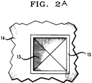
- FIGS. 2 and 2A are a top view of a pyramidal depression within which a ball lens can be mounted;
- FIG. 3 is a view of the apparatus of FIG. 1 at a subsequent stage of its operation; and
- FIG. 4 is a perspective view showing how an optical fiber can be mounted in a V-groove.
- Referring now to FIG. 1, there is shown schematically a placement and bonding
apparatus 11 for picking up a curved optical element, illustratively aball lens 12, placing it at a proper location such as in adepression 13 of a silicon substrate 14, and bonding it to the substrate in accordance with an illustrative embodiment of the invention. Thedepression 13 is illustratively made by etching into a properly mounted crystalline silicon substrate to make a pyramid-shaped depression, a top view of which is shown in FIG. 2. The sidewalls can be very precisely located using known techniques of masking and etching and may be coated with athin layer 15 of aluminum. - The
apparatus 11 comprises abonding tool 16 which is surrounded by a retractingelement holder 17. Avacuum channel 18 in the bonding tool communicates with avacuum source 19 to apply a partial vacuum in agap 20 between thebonding tool 16 and theelement holder 17. A solenoid winding 22 surrounds a portion of the placement andbonding tool 11 which, when activated, causes a retraction of theelement holder 17 to a higher vertical location within theapparatus 11, as shown in FIG. 3. - The
apparatus 11 is preferably part of a robotic apparatus controlled by acomputer 23. It is moveable in X, Y and vertical directions by a motor or motors shown schematically at 24, controlled by thecomputer 23. In operation,apparatus 11 would normally be moved first to a tray of ball lenses.Tool 17 contacts a ball lens, with the vacuum activated by thecomputer 23 through avalve 25, to cause theball lens 12 to adhere to theelement holder 17. Theapparatus 11 then is moved to a location over thedepression 13 of the substrate 14, as shown in FIG. 1. Theball lens 12 may typically be three hundred microns in diameter, and it is therefore difficult to center the ball lens exactly at the apex of thepyramidal depression 13, required for thermo-compression bonding of the ball lens to the substrate. Therefore, in accordance with the invention, after rough placement, as shown in FIG. 1, which may not be precisely centered with respect to thedepression 13, the vacuum is released by operation of thevalve 25, whereupon theball lens 12 is allowed to drop by gravity into thedepression 13. - Referring to FIG. 3, simultaneously with the release of the vacuum, the computer actuates
solenoid 22 to retractholder 17 in a vertical upward direction, as shown. This retracting allows a lower horizontal surface of thebonding tool 16 to make contact with theball lens 12. Thereafter, the computer actuatesmotor 24 to cause theapparatus 11 to move vertically downwardly. - It can be shown that successful thermo-compression bonding of glass to aluminum simply requires the simultaneous application of heat and pressure. The substrate 14 may be heated by a heater schematically shown at 10, while pressure on the ball is provided by the
bonding tool 16 exerting a downward force on theball lens 12. With a spherical glass lens having a diameter of three hundred microns, the applied force may be six hundred grams, and the heat applied may be sufficient to raise the temperature of the substrate 14 to three hundred fifty degrees Centigrade. The pressure may be applied for three seconds to effect the thermo-compression bond. Thereafter, thecomputer 23 causes theapparatus 11 to rise from theball lens 12 and to commence another cycle of operation. - It should be noted if downward force were applied by the
element holder 17 as shown in FIG. 1, the forces would not be properly distributed against opposing sidewalls ofdepression 13, theball lens 12 would not be properly centered, and reliable bonds to the sidewalls would not be formed; thus, release of thelens 12 into the depression prior to bonding is required. After release, theball lens 12 centers itself by gravity. Thereafter, the bottom horizontal surface ofbonding tool 16 should have a sufficient area to insure contact with the centered ball lens. That is, if the positioning accuracy of the tool is, say, five microns, the length and width of the lower surface ofbonding tool 16 should be at least ten microns to insure contact of the bonding tool to the ball lens after centering. As can be appreciated from FIG. 2, the bonding tool applies force that is equally distributed to threeopposing sidewalls 15. - If so desired, the substrate 14 may contain intersecting V-grooves (not shown) for the purpose of defining the position of
ball lens 12. Alternatively, as shown in FIG. 4, theelement 12 may constitute anoptical fiber 12′ which is mounted in a V-groove 13′. In apparatus that we have built, surfaces 28 (FIG. 3) ofholder element 17 were flat and could accommodate both spherical glass balls and cylindrical optical fibers. Alternatively, thesurfaces 28 could be made to match the surfaces only of a cylinder or only of a sphere if so desired. Theapparatus 11 which was built and tested was operated as part of a Seiko XY3000 robot, commercially available from Seiko Instrument, Ltd., Torrance, California. - It can be shown that acoustic energy can be used as an alternative to heat in the bonding step. The invention is also applicable to other methods of bonding using various solders and adhesives. Where epoxy adhesive is used, for example, downward pressure on the optical element is often required for centering the element, seating it, and redistributing the fluid epoxy. Likewise, the use of various solders requires a downward force to insure reliable seating and bonding. Thus, an embodiment using an adhesive is identical to the illustrative embodiment except that, prior to deposit of the ball lens, either the ball lens or the sidewalls are coated with a fluid adhesive and, after the operation, the adhesive is allowed to harden. An embodiment using solder is identical to the illustrative embodiment except that, prior to deposit of the ball lens, either the lens or the sidewalls are coated with solder which after deposit is heated to a fluid condition and, after the operation, is cooled and allowed to be hardened. Various other embodiments and modifications may be made by those skilled in the art without departing from the spirit and scope of the invention.
Claims (11)
- A method for bonding a curved element (12) to slanted opposing sidewalls (15) of a substrate (14) comprising the steps of:
providing a retracting element holder (17) surrounding a bonding tool (16);
providing a vacuum channel (18) communicating with the holder;
contacting the holder to the element and applying a vacuum to the vacuum channel to cause the element to adhere to the holder;
moving the element to a location above the slanted opposing sidewalls of the substrate;
releasing the vacuum, thereby to allow the element to nest between opposing sidewalls;
causing the holder to retract vertically upwardly so as to expose a bonding surface of the bonding tool;
and lowering the bonding tool (16) to contact the element (12) and force it against the opposing sidewalls. - The method of claim 1 wherein:
the element has a substantially circular cross section;
the slanted opposing sidewalls form substantially a V-shaped configuration, whereby when the vacuum is released, the element nests symmetrically with respect to the V-shape;
and the surface of the bonding tool that contacts the element is a substantially flat horizontal surface. - The method of claim 2 wherein:
the element is a cylindrical optical fiber (12′) having a central axis;
the slanted sidewalls define a V-shaped channel;
and when the vacuum is released, at least part of the optical fiber nests in the channel with its central axis parallel to said channel. - The method of claim 2 wherein:
the element is a spherical glass ball;
the slanted sidewalls define a pyramid-shaped depression (13) in the substrate;
and when the vacuum is released, the glass ball nests in the depression with its surface contacting three opposing sidewalls. - The method of claim 1 wherein:
the sidewalls are coated with aluminum (15);
the curved element has an outer surface of glass;
and the sidewalls are heated during the lowering of the bonding tool step. - The method of claim 5 wherein:
the sidewalls are heated to a temperature of approximately three hundred fifty degrees Centigrade;
and during the lowering step, the bonding tool is pressed against the curved element with a force of approximately six hundred grams. - The method of claim 1 wherein:
a first part of the vacuum channel extends through the interior of the bonding tool and a second portion of the vacuum channel is defined between an inner surface of the element holder and an outer surface of the bonding tool. - The method of claim 1 wherein:
an adhesive is provided between the element and the sidewalls to aid in bonding the element to the sidewalls. - The method of claim 1 wherein:
a solder is provided between the element and the sidewalls and is heated to a fluid condition prior to lowering the bonding tool. - The method of claim 6 wherein:
the element is a spherical glass ball;
the slanted sidewalls define a pyramid-shaped depression in the substrate;
and when the vacuum is released, the glass ball nests in the depression and contacts three opposing sidewalls. - The method of claim 5 wherein:
the element is a cylindrical optical fiber having a central axis;
the slanted sidewalls define a V-shaped channel;
and when the vacuum is released, at least part of the optical fiber nests in the channel with its central axis parallel to said channel.
Applications Claiming Priority (2)
| Application Number | Priority Date | Filing Date | Title |
|---|---|---|---|
| US752140 | 1991-08-29 | ||
| US07/752,140 US5194105A (en) | 1991-08-29 | 1991-08-29 | Placement and bonding technique for optical elements |
Publications (2)
| Publication Number | Publication Date |
|---|---|
| EP0529953A1 true EP0529953A1 (en) | 1993-03-03 |
| EP0529953B1 EP0529953B1 (en) | 1995-11-15 |
Family
ID=25025063
Family Applications (1)
| Application Number | Title | Priority Date | Filing Date |
|---|---|---|---|
| EP92307623A Expired - Lifetime EP0529953B1 (en) | 1991-08-29 | 1992-08-20 | Placement and bonding technique |
Country Status (5)
| Country | Link |
|---|---|
| US (1) | US5194105A (en) |
| EP (1) | EP0529953B1 (en) |
| JP (1) | JPH07104469B2 (en) |
| KR (1) | KR930004778A (en) |
| DE (1) | DE69206078T2 (en) |
Cited By (5)
| Publication number | Priority date | Publication date | Assignee | Title |
|---|---|---|---|---|
| EP0631162A1 (en) * | 1993-06-25 | 1994-12-28 | AT&T Corp. | Optical fiber bonding techniques |
| WO2001067149A3 (en) * | 2000-03-03 | 2002-08-29 | Axsun Tech Inc | Bonder chuck and optical component mounting structure |
| EP1327899A1 (en) * | 2002-01-07 | 2003-07-16 | Alcatel | A method for manufacturing an optical module and an optical module |
| US7325306B2 (en) | 2003-11-18 | 2008-02-05 | Rolls-Royce Plc | Method of manufacturing a fibre reinforced metal matrix composite article and a cassette for use therein |
| WO2016045873A1 (en) * | 2014-09-22 | 2016-03-31 | Bayerische Motoren Werke Aktiengesellschaft | Method for welding a ball onto a first component, and method for connecting two components |
Families Citing this family (19)
| Publication number | Priority date | Publication date | Assignee | Title |
|---|---|---|---|---|
| JPH0629577A (en) * | 1992-07-10 | 1994-02-04 | Sumitomo Electric Ind Ltd | Method for manufacturing semiconductor light emitting device |
| US5415730A (en) * | 1993-12-14 | 1995-05-16 | At&T Corp. | Metal coated optical fiber techniques |
| FR2716012B1 (en) * | 1994-02-09 | 1996-04-12 | Corning Inc | Method and device for assembling ends of optical fibers arranged in a sheet. |
| JPH08162455A (en) * | 1994-12-06 | 1996-06-21 | Toshiba Corp | Spherical electrode forming method and forming apparatus |
| US5881193A (en) * | 1995-12-22 | 1999-03-09 | Lucent Technologies Inc. | Low profile optical subassembly |
| US5801681A (en) * | 1996-06-24 | 1998-09-01 | Sayag; Michel | Method and apparatus for generating a control signal |
| EP0900364A1 (en) | 1996-05-14 | 1999-03-10 | Michel Sayag | Method and apparatus for generating a control signal |
| EP0895111A1 (en) * | 1997-07-22 | 1999-02-03 | Lucent Technologies Inc. | Bonding of aluminum oxide components to silicon substrates |
| DE19852345A1 (en) * | 1998-11-13 | 2000-05-18 | Daimler Chrysler Ag | Device and method for applying optical fibers |
| EP1186920A1 (en) | 2000-09-08 | 2002-03-13 | Corning Incorporated | Tool and method for positioning optical fiber arrays |
| US6798970B1 (en) * | 2001-02-26 | 2004-09-28 | Zygo Corporation | Automated placement of optical fibers |
| JPWO2006134675A1 (en) * | 2005-06-14 | 2009-01-08 | 日本電信電話株式会社 | Optical multiplexer / demultiplexer and assembly apparatus therefor |
| DK176290B1 (en) * | 2005-11-14 | 2007-06-11 | Lm Glasfiber As | Removable injection channels during the manufacture of laminates |
| JP5287741B2 (en) * | 2010-01-21 | 2013-09-11 | 富士通株式会社 | Component mounter and component mounting method |
| JP6031946B2 (en) * | 2012-10-31 | 2016-11-24 | コニカミノルタ株式会社 | Lens barrel manufacturing method |
| US20150179854A1 (en) * | 2013-12-19 | 2015-06-25 | Atomic Energy Council - Institute Of Nuclear Energy Research | Method of packaging ball lens of solar collector and structure thereof |
| US10197751B2 (en) * | 2016-03-17 | 2019-02-05 | Applied Optoelectronics, Inc. | Coaxial transmitter optical subassembly (TOSA) including ball lens |
| US10418777B2 (en) | 2017-05-10 | 2019-09-17 | Applied Optoelectronics, Inc. | Coaxial transmitter optical subassembly (TOSA) including side-by-side laser diode and monitor photodiode arrangement |
| WO2025034956A2 (en) * | 2023-08-09 | 2025-02-13 | Ram Photonics Industrial, Llc | Systems and methods for a vacuum gripper assembly |
Citations (2)
| Publication number | Priority date | Publication date | Assignee | Title |
|---|---|---|---|---|
| US4634043A (en) * | 1984-09-20 | 1987-01-06 | At&T Technologies, Inc. | Engaging second articles to engaged first articles |
| WO1988009948A1 (en) * | 1987-06-05 | 1988-12-15 | Siemens Aktiengesellschaft | Process for inserting an optical component in a receiving bore of a support |
Family Cites Families (10)
| Publication number | Priority date | Publication date | Assignee | Title |
|---|---|---|---|---|
| FR2534386A1 (en) * | 1982-10-08 | 1984-04-13 | Socapex | DEVICE FOR MOUNTING OPTICAL FIBERS IN A TIP |
| DE3244689A1 (en) * | 1982-11-30 | 1984-05-30 | Siemens AG, 1000 Berlin und 8000 München | DEVICE FOR LOCAL POSITIONING OF THE FIBER-FIBER ENDS OF FOCUS COMPONENTS |
| US4623156A (en) * | 1984-01-31 | 1986-11-18 | Raychem Corporation | Optical fiber chuck |
| CA1255382A (en) * | 1984-08-10 | 1989-06-06 | Masao Kawachi | Hybrid optical integrated circuit with alignment guides |
| US4904936A (en) * | 1986-03-03 | 1990-02-27 | Emhart Industries, Inc. | Automotive wheel speed sensor including ferromagnetic flux carrying cup closing an opening in the wheel bearing housing |
| GB8714175D0 (en) * | 1987-06-17 | 1987-07-22 | Dynapert Precima Ltd | Suction pick-up apparatus |
| US4892374A (en) * | 1988-03-03 | 1990-01-09 | American Telephone And Telegraph Company, At&T Bell Laboratories | Article comprising an opto-electronic device and an optical waveguide coupled thereto, and method of making the article |
| US4887351A (en) * | 1988-09-09 | 1989-12-19 | Universal Instruments Corporation | Pick and place nozzle with concentric grooves |
| US5124281A (en) * | 1990-08-27 | 1992-06-23 | At&T Bell Laboratories | Method of fabricating a photonics module comprising a spherical lens |
| US5113578A (en) * | 1990-11-29 | 1992-05-19 | Emhart Inc. | Tool tip assembly for surface mount machine |
-
1991
- 1991-08-29 US US07/752,140 patent/US5194105A/en not_active Expired - Lifetime
-
1992
- 1992-08-20 DE DE69206078T patent/DE69206078T2/en not_active Expired - Fee Related
- 1992-08-20 EP EP92307623A patent/EP0529953B1/en not_active Expired - Lifetime
- 1992-08-26 JP JP4248966A patent/JPH07104469B2/en not_active Expired - Fee Related
- 1992-08-27 KR KR1019920015450A patent/KR930004778A/en not_active Withdrawn
Patent Citations (2)
| Publication number | Priority date | Publication date | Assignee | Title |
|---|---|---|---|---|
| US4634043A (en) * | 1984-09-20 | 1987-01-06 | At&T Technologies, Inc. | Engaging second articles to engaged first articles |
| WO1988009948A1 (en) * | 1987-06-05 | 1988-12-15 | Siemens Aktiengesellschaft | Process for inserting an optical component in a receiving bore of a support |
Non-Patent Citations (4)
| Title |
|---|
| PATENT ABSTRACTS OF JAPAN vol. 11, no. 201 (P-590)30 June 1987 & JP-A-62 023 003 ( MATSSSHITA ELECTRIC ) * |
| PATENT ABSTRACTS OF JAPAN vol. 6, no. 87 (E-108)(965) 25 May 1982 & JP-A-57 023 283 ( TOKYO SHIBAURA DENKI ) * |
| PATENT ABSTRACTS OF JAPAN vol. 7, no. 198 (P-220)(1343) 2 September 1983 & JP-A-58 098 716 ( HITACHI ) * |
| PATENT ABSTRACTS OF JAPAN vol. 8, no. 133 (P-281)20 June 1984 & JP-A-59 036 214 ( FUJITSU KK ) * |
Cited By (7)
| Publication number | Priority date | Publication date | Assignee | Title |
|---|---|---|---|---|
| EP0631162A1 (en) * | 1993-06-25 | 1994-12-28 | AT&T Corp. | Optical fiber bonding techniques |
| WO2001067149A3 (en) * | 2000-03-03 | 2002-08-29 | Axsun Tech Inc | Bonder chuck and optical component mounting structure |
| EP1327899A1 (en) * | 2002-01-07 | 2003-07-16 | Alcatel | A method for manufacturing an optical module and an optical module |
| US6974719B2 (en) | 2002-01-07 | 2005-12-13 | Avanex Corporation | Method for manufacturing an optical module and optical module |
| US7325306B2 (en) | 2003-11-18 | 2008-02-05 | Rolls-Royce Plc | Method of manufacturing a fibre reinforced metal matrix composite article and a cassette for use therein |
| WO2016045873A1 (en) * | 2014-09-22 | 2016-03-31 | Bayerische Motoren Werke Aktiengesellschaft | Method for welding a ball onto a first component, and method for connecting two components |
| US20170136577A1 (en) * | 2014-09-22 | 2017-05-18 | Bayerische Motoren Werke Aktiengesellschaft | Method for Welding a Ball onto a First Component, and Method for Connecting Two Components |
Also Published As
| Publication number | Publication date |
|---|---|
| JPH07181357A (en) | 1995-07-21 |
| DE69206078T2 (en) | 1996-04-18 |
| US5194105A (en) | 1993-03-16 |
| DE69206078D1 (en) | 1995-12-21 |
| JPH07104469B2 (en) | 1995-11-13 |
| EP0529953B1 (en) | 1995-11-15 |
| KR930004778A (en) | 1993-03-23 |
Similar Documents
| Publication | Publication Date | Title |
|---|---|---|
| EP0529953B1 (en) | Placement and bonding technique | |
| US5007700A (en) | Edge-emitting diode-to-optical fiber coupling technique | |
| US6456766B1 (en) | Optoelectronic packaging | |
| US5388174A (en) | Optical fiber connector techniques | |
| US6879757B1 (en) | Connection between a waveguide array and a fiber array | |
| EP1218787B1 (en) | An optoelectronic assembly and method for fabricating the same | |
| CA1143547A (en) | Process for attaching optical fiber to semiconductor die | |
| US5178723A (en) | Method and apparatus for making optical devices | |
| US6704150B2 (en) | Bonder chuck and optical component mounting structure interface | |
| JP2003529213A (en) | Methods and devices for passive alignment of optical fibers and optoelectronic devices | |
| US20030011899A1 (en) | Method and structure for aligning optical elements | |
| US6618541B2 (en) | Fiber array fabrication | |
| JP5847718B2 (en) | Method for passively aligning an optoelectronic component assembly on a substrate | |
| JP2970543B2 (en) | Optical element alignment method and optical element module | |
| US11215775B2 (en) | Connection features for electronic and optical packaging | |
| US20020069497A1 (en) | Securing an optical component onto a micro bench | |
| CN120143348A (en) | A method for manufacturing a multi-dimensional densely packed optical fiber array, an optical fiber array device, and an assembly | |
| US20070110361A1 (en) | Wafer level integration of multiple optical elements | |
| WO2020142656A1 (en) | Systems and methods for precision placement of components | |
| JP7648955B2 (en) | Optical waveguide substrate, optical device, and method for manufacturing optical device | |
| WO2026047902A1 (en) | Fiber array assembling device | |
| Ngu | Placement and Bonding Technique | |
| Carlisle | Precision Assembly Automation | |
| JPH10253852A (en) | Receptacle type optical fiber array | |
| WO2003040793A1 (en) | Silicon waferboard |
Legal Events
| Date | Code | Title | Description |
|---|---|---|---|
| PUAI | Public reference made under article 153(3) epc to a published international application that has entered the european phase |
Free format text: ORIGINAL CODE: 0009012 |
|
| AK | Designated contracting states |
Kind code of ref document: A1 Designated state(s): DE FR GB IT SE |
|
| 17P | Request for examination filed |
Effective date: 19930819 |
|
| RAP3 | Party data changed (applicant data changed or rights of an application transferred) |
Owner name: AT&T CORP. |
|
| 17Q | First examination report despatched |
Effective date: 19950126 |
|
| GRAA | (expected) grant |
Free format text: ORIGINAL CODE: 0009210 |
|
| AK | Designated contracting states |
Kind code of ref document: B1 Designated state(s): DE FR GB IT SE |
|
| ITF | It: translation for a ep patent filed | ||
| ET | Fr: translation filed | ||
| REF | Corresponds to: |
Ref document number: 69206078 Country of ref document: DE Date of ref document: 19951221 |
|
| PLBE | No opposition filed within time limit |
Free format text: ORIGINAL CODE: 0009261 |
|
| STAA | Information on the status of an ep patent application or granted ep patent |
Free format text: STATUS: NO OPPOSITION FILED WITHIN TIME LIMIT |
|
| 26N | No opposition filed | ||
| PGFP | Annual fee paid to national office [announced via postgrant information from national office to epo] |
Ref country code: SE Payment date: 20000620 Year of fee payment: 9 |
|
| PGFP | Annual fee paid to national office [announced via postgrant information from national office to epo] |
Ref country code: FR Payment date: 20010725 Year of fee payment: 10 |
|
| PGFP | Annual fee paid to national office [announced via postgrant information from national office to epo] |
Ref country code: GB Payment date: 20010726 Year of fee payment: 10 |
|
| PG25 | Lapsed in a contracting state [announced via postgrant information from national office to epo] |
Ref country code: SE Free format text: LAPSE BECAUSE OF NON-PAYMENT OF DUE FEES Effective date: 20010821 |
|
| PGFP | Annual fee paid to national office [announced via postgrant information from national office to epo] |
Ref country code: DE Payment date: 20010928 Year of fee payment: 10 |
|
| REG | Reference to a national code |
Ref country code: GB Ref legal event code: IF02 |
|
| EUG | Se: european patent has lapsed |
Ref document number: 92307623.6 |
|
| PG25 | Lapsed in a contracting state [announced via postgrant information from national office to epo] |
Ref country code: GB Free format text: LAPSE BECAUSE OF NON-PAYMENT OF DUE FEES Effective date: 20020820 |
|
| PG25 | Lapsed in a contracting state [announced via postgrant information from national office to epo] |
Ref country code: DE Free format text: LAPSE BECAUSE OF NON-PAYMENT OF DUE FEES Effective date: 20030301 |
|
| GBPC | Gb: european patent ceased through non-payment of renewal fee |
Effective date: 20020820 |
|
| PG25 | Lapsed in a contracting state [announced via postgrant information from national office to epo] |
Ref country code: FR Free format text: LAPSE BECAUSE OF NON-PAYMENT OF DUE FEES Effective date: 20030430 |
|
| REG | Reference to a national code |
Ref country code: FR Ref legal event code: ST |
|
| PG25 | Lapsed in a contracting state [announced via postgrant information from national office to epo] |
Ref country code: IT Free format text: LAPSE BECAUSE OF NON-PAYMENT OF DUE FEES;WARNING: LAPSES OF ITALIAN PATENTS WITH EFFECTIVE DATE BEFORE 2007 MAY HAVE OCCURRED AT ANY TIME BEFORE 2007. THE CORRECT EFFECTIVE DATE MAY BE DIFFERENT FROM THE ONE RECORDED. Effective date: 20050820 |