EP0527692B1 - Annuleur d'écho lointain - Google Patents
Annuleur d'écho lointain Download PDFInfo
- Publication number
- EP0527692B1 EP0527692B1 EP92420270A EP92420270A EP0527692B1 EP 0527692 B1 EP0527692 B1 EP 0527692B1 EP 92420270 A EP92420270 A EP 92420270A EP 92420270 A EP92420270 A EP 92420270A EP 0527692 B1 EP0527692 B1 EP 0527692B1
- Authority
- EP
- European Patent Office
- Prior art keywords
- memory
- data
- echo canceller
- microcontroller
- far
- Prior art date
- Legal status (The legal status is an assumption and is not a legal conclusion. Google has not performed a legal analysis and makes no representation as to the accuracy of the status listed.)
- Expired - Lifetime
Links
Images


Classifications
-
- H—ELECTRICITY
- H04—ELECTRIC COMMUNICATION TECHNIQUE
- H04B—TRANSMISSION
- H04B3/00—Line transmission systems
- H04B3/02—Details
- H04B3/20—Reducing echo effects or singing; Opening or closing transmitting path; Conditioning for transmission in one direction or the other
- H04B3/23—Reducing echo effects or singing; Opening or closing transmitting path; Conditioning for transmission in one direction or the other using a replica of transmitted signal in the time domain, e.g. echo cancellers
- H04B3/237—Reducing echo effects or singing; Opening or closing transmitting path; Conditioning for transmission in one direction or the other using a replica of transmitted signal in the time domain, e.g. echo cancellers using two adaptive filters, e.g. for near end and for end echo cancelling
Definitions
- the present invention relates to modulators / demodulators (modems) with simultaneous bilateral transmission (duplex) in the same frequency band, on a two-wire line.
- an echo canceller usually has two channels, one close echo cancellation channel linked to the coupler the transmitter and the parts close to the line, and a channel cancellation of distant echoes corresponding for example to a transmission by one or more satellites.
- the echo canceller distant must receive a signal corresponding to the transmitted signal delayed transmission time and echo on satel lites, i.e. for example a duration of the order of second. This involves using a delay line, in practice a memory, with a large storage capacity, for example of the order of 4 kmots for the above-mentioned delay.
- a general purpose microcontroller possibly consisting of the central processor of a personal computer which is attached to the modem, including in particular interface circuits with terminal equipment (DTE) transmitting and receiving data via the modem, a command interpreter DTE, data compression circuits, and error correction ...
- Modem specific functions, and including the echo cancellation function are performed on one or more autonomous integrated circuits including in particular a fast processor to perform calculations very quickly necessary for the implementation of these functions.
- DTE terminal equipment
- the data pump performing the suppressor function must be associated with the aforementioned signal storage memory.
- this memory is a fast memory whose access times are of several orders larger than those necessary for the function fulfilled, for example a SRAM type memory, which occupies a surface relatively large.
- this memory is consisting of an integrated circuit chip separate from the pump data itself. Indeed a monolithic integration would generally lead to too large a chip surface.
- a first drawback is, as has been indicated, to require the provision of a specific external memory.
- a second drawback, related to the first, is that it address and data link between the data pump and its external memory.
- the memory has a dimension of 4 kmots, it will be noted that the addressing must be done on a minimum of 12 bits. This implies that 12 studs must specifically be allocated to this addressing, this which increases the size of the data pump chip.
- An object of the present invention is to provide a new modem architecture including an echo canceller overcoming the aforementioned drawbacks.
- the present invention provides a distant echo canceller for duplex modem comprising at least minus a fast processor constituting an arithmetic and logical unit and realizing filtering operations and a control microcontroller, in which data characteristic of the data transmitted, necessary for the operation of suppressing distant echoes, are stored in a memory managed by the microcontroller.
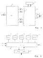
- FIG. 1 shows the main elements of a data pump circuit, usually grouped on one or multiple modem chips.
- This circuit is intended to transmit and receive signals through a coupling circuit 1 connected to a two-wire line 2.
- the transmitter circuit 4 sends Tn signals to the coupler 1.
- These Tn signals are signals having undergone various scrambling and coding treatments and correspond to Din input data.
- the signals received Hn from coupler 1 are transmitted in particular to a echo canceller 6 then to a receiver 8 which decodes them and provides Dout output data.
- Echo canceller 6 receives Sn signals which correspond to the Din data partially or totally processed by the transmitter 4. All of the circuits 4, 6 and 8 is controlled by an external controller providing CONT control signals to an interface circuit 10 which controls receiver and echo canceller and transmitter status signals (STAT) which it sends back to the controller.
- STAT receiver and echo canceller and transmitter status signals
- FIG. 2 very schematically illustrates that echo canceller 6 has two channels, one cancellation channel NEEC 11 near echo, and a far echo cancellation channel FEEC 12.
- the near echo canceller 11 receives almost directly the signals Sn linked to the transmitted signals and the echo canceller far receives these signals Sn through a circuit delay 13.
- Cancellation signals from near and far echoes are added in a first summator 14 then are then added to the signal Hn by the adder 15 to provide the signal without echo.
- Figure 3 shows an aspect of the architecture classic modem.
- the data pump circuits of the Figure 1, designated by the reference 21, are associated with coupler 1, to a memory 22 ensuring the line function at delay designated by the reference 13 in FIG. 2, and to a microcontroller 24 via the interface circuit 10.
- the microcontroller as indicated previously, data exchange with a data terminal to which the modem is associated, via a line or rather of a bus 25.
- the microcontroller generally comprises internal quick memory areas and external memory areas possibly slower.
- FIG. 4 illustrates a practical embodiment under schematic form of an echo canceller.
- This basically includes an arithmetic and logic unit (ALU) or processor fast 30 intended to perform calculations on the Sn data and Hn previously defined.
- ALU arithmetic and logic unit
- the arithmetic unit and logic 30 is associated with various memories, 31 to 35.
- the memory 31 is a memory which contains the operating program ALU 30.
- Memory 32 is a coefficient memory which are used for cancellation operations.
- Memory 33 is a symbol or signal memory for the echo canceller close (NE).
- the memory 34 is a memory for symbols or signals for the far echo canceller (FE).
- Memory 35 corresponds the delay line associated with signal processing distant echo.
- memory 31 will have a capacity of approximately 2 kmots, memories 32 to 34 of capacities of 128 words, and memory 35 serving as line for delay a capacity of around 4 kmots.
- memories 31 to 34 are produced on the same chip as the one that incorporates the arithmetic unit and logic 30, while memory 35, of larger dimension, is usually done on a separate chip to which the arithmetic and logical unit is connected by a large number of pins, since this memory necessarily has a large number of addresses.
- the ALU 30 is clocked by CONT control signals from the microcontroller via interface 10 and returns STAT status signals.
- the present invention is based on an analysis of the classic circuit of Figure 4. We see that in fact the timing of input and output of Hn, Sn and Rn data is very slow compared to the speed at which must be done the calculations concerning the data stored in the memories 32 to 34. On the other hand, the data contained in memory 35 can only be delivered at the same rate as the data Hn, Sn and Rn. Thus, the present invention proposes to use, to store the data intended for the calculation of the far echo, a memory associated not directly with the arithmetic unit and logical but to the microcontroller.
- Figure 5 shows the same elements as those of Figure 4 with the same references. The essential difference is that the delay memory 35 is removed and instead of that, links 37 are provided, 38 to the interface allowing to send to the microcontroller assigned data from virtual addresses and recall these data to these virtual addresses, the microcontroller loading storage management.
- the microcontroller is usually associated with a large memory dimension, for example of the order of 64 kmots to 1 Mmot and it always have enough room in this memory to contain the 4 kmots normally provided in memory 35.
- the communication between the circuit interface 10 and a corresponding interface circuit of the microcontroller can be done on the number of lines normally used to exchange data, control and status, for example on an 8-line bus in which the data is sent in serial form. So thanks to the present invention, the number of connections is not increased between the data pump and the microcontroller and we delete the very many pins necessary for the connection between this data pump and a memory 22 as illustrated in Figure 3 (note that the reference 22 in Figure 3 and the reference 35 of FIG. 4 designate memories having the same function).
- Figure 6 illustrates the overall coupling scheme between the microcontroller and the data pump according to the invention.
- the interface with the microcontroller carries the reference 10 and an analog interface with the coupler 1 carries the reference 40.
- the circuit according to the present invention comprises conversion circuits digital / analog and analog / digital to enable digital data processing in the unit arithmetic and logic 30, and the transmission and reception of data to the two-wire line in analog form.
- the microcontroller 24 includes an arithmetic and logic unit 41, coupled to a program memory 42, for example a ROM type memory, and a data and parameter memory 43, for example a DRAM type memory, which will be used in particular to store the data previously stored in the memory 35.
- Memories 42 and 43 are generally produced partly on the same chip as the microcontroller and for their most of it on external chips according to technologies used.
- the microcontroller also includes a interface circuit 44 to the data pump and a circuit interface 45 to the circuits from which the signals to send and receive on the two-wire line. We have shown as a single bond 47 the bond between interfaces 10 and 44. This connection is for example a serial link, or an 8-bit dual-access memory area, or even a mailbox.
Landscapes
- Engineering & Computer Science (AREA)
- Computer Networks & Wireless Communication (AREA)
- Signal Processing (AREA)
- Cable Transmission Systems, Equalization Of Radio And Reduction Of Echo (AREA)
- Dc Digital Transmission (AREA)
- Transceivers (AREA)
- Bidirectional Digital Transmission (AREA)
Description
Claims (3)
- Annuleur d'écho lointain pour modem duplex comprenant au moins un processeur rapide (30) constituant une unité arithmétique et logique et réalisant des opérations de filtrage et un microcontrôleur de commande (41), caractérisé en ce que des données caractéristiques des données émises, nécessaires pour l'opération de suppression d'échos lointains, sont stockées dans une mémoire (43) gérée par le microcontrôleur.
- Annuleur d'écho lointain selon la revendication 1, caractérisé en ce que ladite mémoire (43) est une mémoire de type DRAM.
- Annuleur d'écho lointain selon la revendication 1, caractérisé en ce que lesdites données caractéristiques arrivent sur le processeur rapide (30) et sont renvoyées vers le microcontrôleur (41) puis rappelées de celui-ci par une interface (10) incluant une mémoire à double accès de faible capacité.
Applications Claiming Priority (2)
| Application Number | Priority Date | Filing Date | Title |
|---|---|---|---|
| FR9110424A FR2680293B1 (fr) | 1991-08-09 | 1991-08-09 | Annuleur d'echo lointain. |
| FR9110424 | 1991-08-09 |
Publications (2)
| Publication Number | Publication Date |
|---|---|
| EP0527692A1 EP0527692A1 (fr) | 1993-02-17 |
| EP0527692B1 true EP0527692B1 (fr) | 1998-04-29 |
Family
ID=9416265
Family Applications (1)
| Application Number | Title | Priority Date | Filing Date |
|---|---|---|---|
| EP92420270A Expired - Lifetime EP0527692B1 (fr) | 1991-08-09 | 1992-08-05 | Annuleur d'écho lointain |
Country Status (5)
| Country | Link |
|---|---|
| US (1) | US5434849A (fr) |
| EP (1) | EP0527692B1 (fr) |
| JP (1) | JPH05206899A (fr) |
| DE (1) | DE69225279T2 (fr) |
| FR (1) | FR2680293B1 (fr) |
Families Citing this family (4)
| Publication number | Priority date | Publication date | Assignee | Title |
|---|---|---|---|---|
| US6031867A (en) | 1993-07-02 | 2000-02-29 | Multi-Tech Systems, Inc. | Modem with firmware upgrade feature |
| US6014371A (en) * | 1997-03-05 | 2000-01-11 | Paradyne Corporation | Echo cancellation system and method for multipoint networks |
| US6138190A (en) * | 1997-09-16 | 2000-10-24 | Cirrus Logic, Inc. | Analog front end and digital signal processing device and method |
| RU2174738C1 (ru) * | 2000-10-31 | 2001-10-10 | ЗАО "НПО "Кросна" | Способ групповой эхокомпенсации и групповой эхокомпенсатор |
Family Cites Families (11)
| Publication number | Priority date | Publication date | Assignee | Title |
|---|---|---|---|---|
| US4742510A (en) * | 1986-04-04 | 1988-05-03 | Massachusetts Institute Of Technology | Near and far echo canceller for data communications |
| JPS63236422A (ja) * | 1987-03-25 | 1988-10-03 | Hitachi Ltd | 二線全二重モデム用エコ−キヤンセラ |
| US4970715A (en) * | 1987-03-27 | 1990-11-13 | Universal Data Systems, Inc. | Modem with improved remote echo location and cancellation |
| US4841561A (en) * | 1987-12-08 | 1989-06-20 | General Datacomm, Inc. | Operating default group selectable data communication equipment |
| US4893305A (en) * | 1988-03-31 | 1990-01-09 | Racal Data Communications Inc. | Inband dynamic port allocation |
| US5005168A (en) * | 1988-05-02 | 1991-04-02 | Itt Corporation | Multirate wire line modem apparatus |
| US5177734A (en) * | 1988-05-02 | 1993-01-05 | Itt Corporation | Multirate wire line modem apparatus |
| US5007047A (en) * | 1988-12-02 | 1991-04-09 | Codex Corporation | Adaptive rate control for echo cancelling modem |
| JP2754825B2 (ja) * | 1989-02-03 | 1998-05-20 | 日本電気株式会社 | マイクロプロセッサ |
| US5029204A (en) * | 1989-10-26 | 1991-07-02 | Dsc Communications Corporation | Operational status controller for echo canceling |
| US5214637A (en) * | 1991-04-15 | 1993-05-25 | Codex Corporation | High speed two wire modem |
-
1991
- 1991-08-09 FR FR9110424A patent/FR2680293B1/fr not_active Expired - Fee Related
-
1992
- 1992-08-03 JP JP4224578A patent/JPH05206899A/ja active Pending
- 1992-08-05 EP EP92420270A patent/EP0527692B1/fr not_active Expired - Lifetime
- 1992-08-05 DE DE69225279T patent/DE69225279T2/de not_active Expired - Fee Related
- 1992-08-07 US US07/926,813 patent/US5434849A/en not_active Expired - Lifetime
Non-Patent Citations (1)
| Title |
|---|
| Modem Data Book and Applications, 1ère édition, Mai 1989, de SGS-THOMSON Microelectronics (ST), pages 140, 141 * |
Also Published As
| Publication number | Publication date |
|---|---|
| US5434849A (en) | 1995-07-18 |
| DE69225279T2 (de) | 1998-08-20 |
| DE69225279D1 (de) | 1998-06-04 |
| JPH05206899A (ja) | 1993-08-13 |
| FR2680293A1 (fr) | 1993-02-12 |
| FR2680293B1 (fr) | 1993-11-12 |
| EP0527692A1 (fr) | 1993-02-17 |
Similar Documents
| Publication | Publication Date | Title |
|---|---|---|
| EP1044436B1 (fr) | Procede de communication entre une station d'utilisateur et un reseau, notamment du type internet, et architecture de mise en oeuvre | |
| BE1000396A7 (fr) | Systeme de commutation. | |
| US4785473A (en) | Interactive audio telecommunications message storage, forwarding and retrieval system | |
| EP0524070B1 (fr) | Dispositif universel de couplage d'un bus d'ordinateur à un contrôleur d'un groupe de périphériques | |
| FR2732536A1 (fr) | Microregisseur traitant les informations relatives au demandeur dans un dispositif de telecommunications, et procede de commande de l'alimentation electrique utilisee dans ce regisseur | |
| EP2215820B1 (fr) | Procédé et agencement pour une annulation d'écho dans des signaux vocaux | |
| FR2693575A1 (fr) | Carte à mémoire de masse avec fonction entrée/sortie. | |
| EP0700192A1 (fr) | Enregistreur numérique de signaux sonores compressés | |
| FR2670925A1 (fr) | Architecture informatique distribuee utilisant un reseau local de type csma/cd. | |
| EP0171856B1 (fr) | Processeur pour le traitement de signal et structure de multitraitement hiérarchisée comportant au moins un tel processeur | |
| EP0527692A1 (fr) | Annuleur d'écho lointain | |
| EP0920157A1 (fr) | Dispositif de gestion de mémoire tampon partagée | |
| EP0054329A1 (fr) | Annuleur d'écho pour transmission téléphonique par voies numériques mettant en oeuvre une loi de codage pseudo-logarithmique | |
| FR2627647A1 (fr) | Filtre numerique a decimation integree | |
| CA2132594C (fr) | Systeme de transmission de donnees par satellite entre centres de commutation telephoniques, station de trafic et procede de transmission correspondants | |
| US7085245B2 (en) | Coefficient domain history storage of voice processing systems | |
| EP0275790B1 (fr) | Terminal de transmission de données sur une voie analogique bidirectionnelle avec annulation d'écho couplée au rythme réception | |
| EP0178205B1 (fr) | Réseau numérique à accès multiples | |
| EP0304362B1 (fr) | Dispositif de calcul numérique pour installation de transmission de données en code 2B 1Q ou analogue | |
| JP3013613B2 (ja) | データ送受信装置 | |
| US6014371A (en) | Echo cancellation system and method for multipoint networks | |
| EP0441707B1 (fr) | Coupleur de bus série | |
| FR2489061A1 (fr) | Systeme de transmission d'images utilisant un dispositif de restitutions de points | |
| US8565416B2 (en) | Cache-based echo canceller | |
| FR2524750A1 (fr) | Systeme de visioconference multisalle |
Legal Events
| Date | Code | Title | Description |
|---|---|---|---|
| PUAI | Public reference made under article 153(3) epc to a published international application that has entered the european phase |
Free format text: ORIGINAL CODE: 0009012 |
|
| AK | Designated contracting states |
Kind code of ref document: A1 Designated state(s): DE FR GB IT |
|
| 17P | Request for examination filed |
Effective date: 19930722 |
|
| 17Q | First examination report despatched |
Effective date: 19960913 |
|
| GRAG | Despatch of communication of intention to grant |
Free format text: ORIGINAL CODE: EPIDOS AGRA |
|
| GRAG | Despatch of communication of intention to grant |
Free format text: ORIGINAL CODE: EPIDOS AGRA |
|
| GRAH | Despatch of communication of intention to grant a patent |
Free format text: ORIGINAL CODE: EPIDOS IGRA |
|
| GRAH | Despatch of communication of intention to grant a patent |
Free format text: ORIGINAL CODE: EPIDOS IGRA |
|
| GRAA | (expected) grant |
Free format text: ORIGINAL CODE: 0009210 |
|
| AK | Designated contracting states |
Kind code of ref document: B1 Designated state(s): DE FR GB IT |
|
| REF | Corresponds to: |
Ref document number: 69225279 Country of ref document: DE Date of ref document: 19980604 |
|
| GBT | Gb: translation of ep patent filed (gb section 77(6)(a)/1977) |
Effective date: 19980605 |
|
| ITF | It: translation for a ep patent filed | ||
| RAP4 | Party data changed (patent owner data changed or rights of a patent transferred) |
Owner name: STMICROELECTRONICS S.A. |
|
| PLBE | No opposition filed within time limit |
Free format text: ORIGINAL CODE: 0009261 |
|
| 26N | No opposition filed | ||
| PGFP | Annual fee paid to national office [announced via postgrant information from national office to epo] |
Ref country code: DE Payment date: 20000729 Year of fee payment: 9 |
|
| PGFP | Annual fee paid to national office [announced via postgrant information from national office to epo] |
Ref country code: GB Payment date: 20000802 Year of fee payment: 9 |
|
| PGFP | Annual fee paid to national office [announced via postgrant information from national office to epo] |
Ref country code: FR Payment date: 20000811 Year of fee payment: 9 |
|
| PG25 | Lapsed in a contracting state [announced via postgrant information from national office to epo] |
Ref country code: GB Free format text: LAPSE BECAUSE OF NON-PAYMENT OF DUE FEES Effective date: 20010805 |
|
| GBPC | Gb: european patent ceased through non-payment of renewal fee |
Effective date: 20010805 |
|
| PG25 | Lapsed in a contracting state [announced via postgrant information from national office to epo] |
Ref country code: FR Free format text: LAPSE BECAUSE OF NON-PAYMENT OF DUE FEES Effective date: 20020430 |
|
| PG25 | Lapsed in a contracting state [announced via postgrant information from national office to epo] |
Ref country code: DE Free format text: LAPSE BECAUSE OF NON-PAYMENT OF DUE FEES Effective date: 20020501 |
|
| REG | Reference to a national code |
Ref country code: FR Ref legal event code: ST |
|
| PG25 | Lapsed in a contracting state [announced via postgrant information from national office to epo] |
Ref country code: IT Free format text: LAPSE BECAUSE OF NON-PAYMENT OF DUE FEES;WARNING: LAPSES OF ITALIAN PATENTS WITH EFFECTIVE DATE BEFORE 2007 MAY HAVE OCCURRED AT ANY TIME BEFORE 2007. THE CORRECT EFFECTIVE DATE MAY BE DIFFERENT FROM THE ONE RECORDED. Effective date: 20050805 |