EP0525424B1 - Liquid crystal spatial light modulator - Google Patents
Liquid crystal spatial light modulator Download PDFInfo
- Publication number
- EP0525424B1 EP0525424B1 EP92111152A EP92111152A EP0525424B1 EP 0525424 B1 EP0525424 B1 EP 0525424B1 EP 92111152 A EP92111152 A EP 92111152A EP 92111152 A EP92111152 A EP 92111152A EP 0525424 B1 EP0525424 B1 EP 0525424B1
- Authority
- EP
- European Patent Office
- Prior art keywords
- liquid crystal
- image
- light
- optical
- ferroelectric liquid
- Prior art date
- Legal status (The legal status is an assumption and is not a legal conclusion. Google has not performed a legal analysis and makes no representation as to the accuracy of the status listed.)
- Expired - Lifetime
Links
Images


Classifications
-
- G—PHYSICS
- G02—OPTICS
- G02F—OPTICAL DEVICES OR ARRANGEMENTS FOR THE CONTROL OF LIGHT BY MODIFICATION OF THE OPTICAL PROPERTIES OF THE MEDIA OF THE ELEMENTS INVOLVED THEREIN; NON-LINEAR OPTICS; FREQUENCY-CHANGING OF LIGHT; OPTICAL LOGIC ELEMENTS; OPTICAL ANALOGUE/DIGITAL CONVERTERS
- G02F1/00—Devices or arrangements for the control of the intensity, colour, phase, polarisation or direction of light arriving from an independent light source, e.g. switching, gating or modulating; Non-linear optics
- G02F1/01—Devices or arrangements for the control of the intensity, colour, phase, polarisation or direction of light arriving from an independent light source, e.g. switching, gating or modulating; Non-linear optics for the control of the intensity, phase, polarisation or colour
- G02F1/13—Devices or arrangements for the control of the intensity, colour, phase, polarisation or direction of light arriving from an independent light source, e.g. switching, gating or modulating; Non-linear optics for the control of the intensity, phase, polarisation or colour based on liquid crystals, e.g. single liquid crystal display cells
- G02F1/133—Constructional arrangements; Operation of liquid crystal cells; Circuit arrangements
- G02F1/135—Liquid crystal cells structurally associated with a photoconducting or a ferro-electric layer, the properties of which can be optically or electrically varied
-
- G—PHYSICS
- G06—COMPUTING; CALCULATING OR COUNTING
- G06V—IMAGE OR VIDEO RECOGNITION OR UNDERSTANDING
- G06V10/00—Arrangements for image or video recognition or understanding
- G06V10/88—Image or video recognition using optical means, e.g. reference filters, holographic masks, frequency domain filters or spatial domain filters
-
- G—PHYSICS
- G02—OPTICS
- G02F—OPTICAL DEVICES OR ARRANGEMENTS FOR THE CONTROL OF LIGHT BY MODIFICATION OF THE OPTICAL PROPERTIES OF THE MEDIA OF THE ELEMENTS INVOLVED THEREIN; NON-LINEAR OPTICS; FREQUENCY-CHANGING OF LIGHT; OPTICAL LOGIC ELEMENTS; OPTICAL ANALOGUE/DIGITAL CONVERTERS
- G02F1/00—Devices or arrangements for the control of the intensity, colour, phase, polarisation or direction of light arriving from an independent light source, e.g. switching, gating or modulating; Non-linear optics
- G02F1/01—Devices or arrangements for the control of the intensity, colour, phase, polarisation or direction of light arriving from an independent light source, e.g. switching, gating or modulating; Non-linear optics for the control of the intensity, phase, polarisation or colour
- G02F1/13—Devices or arrangements for the control of the intensity, colour, phase, polarisation or direction of light arriving from an independent light source, e.g. switching, gating or modulating; Non-linear optics for the control of the intensity, phase, polarisation or colour based on liquid crystals, e.g. single liquid crystal display cells
- G02F1/137—Devices or arrangements for the control of the intensity, colour, phase, polarisation or direction of light arriving from an independent light source, e.g. switching, gating or modulating; Non-linear optics for the control of the intensity, phase, polarisation or colour based on liquid crystals, e.g. single liquid crystal display cells characterised by the electro-optical or magneto-optical effect, e.g. field-induced phase transition, orientation effect, guest-host interaction or dynamic scattering
- G02F1/139—Devices or arrangements for the control of the intensity, colour, phase, polarisation or direction of light arriving from an independent light source, e.g. switching, gating or modulating; Non-linear optics for the control of the intensity, phase, polarisation or colour based on liquid crystals, e.g. single liquid crystal display cells characterised by the electro-optical or magneto-optical effect, e.g. field-induced phase transition, orientation effect, guest-host interaction or dynamic scattering based on orientation effects in which the liquid crystal remains transparent
- G02F1/141—Devices or arrangements for the control of the intensity, colour, phase, polarisation or direction of light arriving from an independent light source, e.g. switching, gating or modulating; Non-linear optics for the control of the intensity, phase, polarisation or colour based on liquid crystals, e.g. single liquid crystal display cells characterised by the electro-optical or magneto-optical effect, e.g. field-induced phase transition, orientation effect, guest-host interaction or dynamic scattering based on orientation effects in which the liquid crystal remains transparent using ferroelectric liquid crystals
Definitions
- the present invention relates to an optically writable spatial light modulator of an liquid crystal type according to the preamble of claim 1 as well as to a driving method thereof, which may be utilized in an image processing device and an optical information processing device.
- a driving method thereof which may be utilized in an image processing device and an optical information processing device.
- Such an optically writable spatial light modulator as well as its driving method are for example known from Applied Optics, vol. 28, no. 22, November 1989, New York, US; pages 4763-4771, D. Armitage et al.: "Photoaddressed liquid crystal SLM" which is mainly concerned with the use of nematic liquid crystals.
- the present invention focusses on a liquid crystal type composed of a ferroelectric liquid crystal type having optical bistability.
- the spatial light modulator of the ferroelectric liquid crystal type is utilized as an optical device for modulating an intensity of inputted image information on real time basis to output the modulated result.
- the outputted image is a binarized form of the inputted image.
- the inventors have disclosed a method of driving the above noted optical modulator to produce an output image having a continuous gradation in Japanese Patent No. 4 119 318.
- an object of the present invention is to directly obtain an edge enhancement function useful in the optical information processing technology and to produce an edge extracted image without using a peculiar device structure.
- the ferroelectric liquid crystal layer is thinned such that its layer thickness is reduced less than a natural helical pitch so that liquid crystal molecules align in a single crystal texture from the spiral texture.
- This single crystal texture develops bistable performance such that when a bipolar pulse voltage or a square waveform voltage having a magnitude greater than a threshold level is applied to the liquid crsytal layer, a spontaneous polarization of the liquid crystal strongly couples with an electric field of the applied voltage.
- the optically switchable spatial light modulator of the ferroelectric liquid crystal type combined with the photoconductive film has basically the same performance. Namely, the magnitude of the applied voltage, an intensity of the readout light and an intensity of the write light are suitably set so that an optical input image of binary data is written and memorized as it is in the binarized form.
- the binary drive using a pulse voltage is effected so that the written image is binarized and memorized according to a pulse threshold voltage.
- a gradative drive may be effected with using a square waveform voltage superposed with a DC bias voltage so as to read out a gradated image corresponding to an intensity distribution of the input image.
- the inventive spatial light modulator of the ferroelectric liquid crystal type is constructed such that a reading optical system is set in a crossed-Nicols mode and a polarization axis of linearly polarized incident light thereof is oriented along an intermediate direction between a pair of optical axes of bistable states of the ferroelectric liquid crystal, or the polarization axis is oriented perpendicular to the intermediate direction.
- a bipolar pulse is applied while continuously irradiating a writing light and a reading light to drive the modulator to thereby directly produce an edge enhanced or edge extracted image which would be useful for the optical information processing.
- the intensity of the reading light can be increased without affecting the writing performance of the spatial light modulator because the photoconductive film is not irradiated by the readout light, thereby producing a bright and clear read output image.
- the modulator is applied sequentially with a first pulse voltage effective to erase or reset an image, a second pulse voltage having an opposite polarity to that of the first pulse voltage for writing an image, and a third pulse voltage having the same polarity as that of the first pulse voltage for erasing a part of the written image except for an edge thereof to thereby memorize an edge enhanced image.
- the writing light and the readout light are continuously irradiated to optically input image information so as to directly produce the edge enhanced or edge extracted image useful in the optical information processing technology.
- the spatial light modulator of the ferroelectric liquid crystal type is operated such that, the readout optical system is set in the crossed-Nicols mode and the polarization axis of the linearly polarized incident light is oriented along an intermediate direction between a pair of optical axes of the bistable states of the ferroelectric liquid crystal or the polarization axis is oriented perpendicular to the intermediate direction.
- the pulses of the opposite polarities are applied while the write light and the readout light are continuously irradiated so as to drive the modulator.
- a transmitting light intensity through one stable state of the ferroelectric liquid crystal molecules in the erased state can be equalized to another transmitting light intensity through another stable state of the ferroelectric liquid crystal molecules which are reversed by the writing operation.
- image information is written by the writing light so that the ferroelectric liquid crystal layer contains two different regions of the bistable states after erasing. According to the invention, these two regions are optically equivalent; however, an irregular zone is left along a boundary between the two regular regions such that the ferroelectric liquid crystal molecules are not aligned uniaxially in the irregular zone. This irregular zone is read out according to the invention, hence the boundary zone is optically different from the remaining regions, thereby obtaining an output image comprised solely of an extracted edge line.
- the second pulse voltage of the opposite polarity is applied to effect the binary writing of an given image.
- an electric carrier is generated initially in the vicinity of an input surface of the photoconductive film.
- the carrier moves vertically through the photoconductive film to thereby apply an electric field to the ferroelectric liquid crystal layer to induce an inversion of the liquid crystal molecules, while the carrier migrates or diffuses horizontally along input and output surfaces of the photoconductive film.
- the written or recorded image is slightly enlarged relative to the original input image due to the horizontal diffusion of the carrier. This is observed similarly in case that a gradated input image is recorded in a binarized form.
- the polarity of the applied electric field is set such that an electron moves to the ferroelectric liquid crystal layer.
- the effective carrier is the electron in the writing operation.
- the third pulse voltage of the same polarity as that of the first pulse voltage is applied to erase a major part of the written image except for an edge portion so as to memorized an edge enhanced image.
- a carrier moves vertically in manner similar to that moment when the second pulse voltage is applied. Since the polarity is opposite, the moving carrier is composed of holes so that the horizontal diffusion degree thereof is smaller than that when the second pulse voltage is applied. When the hole reaches a boundary to the ferroelectric liquid crystal layer, the written image is erased within an activated region.
- the horizontal diffusion degree is slightly reduced while the input image is not changed during the course of switching between the second and third pulses, hence the modulator extracts and memorizes an edge of the input image, which corresponds to the horizontally enlarged zone of the written image recorded by the application of the second pulse.
- the spatial light modulator of the ferroelectric liquid crystal type is operated according to the inventive driving method to produce directly the edge enhanced or edge extracted image which would be useful in the optical information processing.
- Fig. 1 is a diagram showing relative settings of molecular axis directions of ferroelectric liquid crystal molecules in bistable states and polarization axes of polarizer and analyzer of a reading optical system in the inventive spatial light modulator of ferroelectric liquid crystal.
- Fig. 2 is a schematic diagram showing the principle of edge enhancement operation according to the invention.
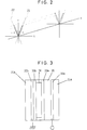
- Fig. 3 is a schematic diagram showing a structure of the inventive spatial light modulator.
- Fig. 4 is a system diagram of the optical system for writing and reading operations.
- Fig. 5 (A) and Fig. 5(B) are characteristic diagrams showing a driving waveform of the inventive spatial light modulator and an optical response of the spatial light modulator set in a crossed-Nicols condition respectively.
- Fig. 6 is a schematic illustration explaining the principle of edge enhancement operation according to the invention.
- Fig. 7 is a schematic illustration showing the principle of edge emhancement operation according to the invention.
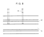
- Fig. 8 is a schematic illustration showing the principle of edge enhancement operation according to the invention.
- Fig. 3 is a schematic diagram showing a light volve used in an optically writable mode spatial light modulator of the ferroelectric liquid crystal type according to the invention.
- Liquid crystal molecules are sandwiched by a pair of substrates 31a and 31b which are comprised of a transparent glass plate having a thickness of 5 mm and being polished both faces to ensure a parallel flatness of less than ⁇ /5 where ⁇ denotes a wavelength of He-Ne laser beam.
- ITO transparent electrode layers 32a, 32b are formed on surfaces of the respective substrates.
- the one transparent electrode layer 32a is disposed at an optical writing side, and is formed thereon with a photoconductive layer 35 having 2.5 ⁇ m of thickness composed of hydrogenated amorphous silicon (a-Si:H).
- alignment layers 33a, 33b are formed on the respective substrates such that silicon monooxide is obliquely evaporated at an incident angle of 85 relative to a normal of each substrate and that respective incident angles are coincident with each other between the writing and reading sides after the pair of substrates are coupled to one another.
- the pair of substrates are fixed to each other through a peripheral sealer which is applied by relief printing method.
- the sealer contains therein dispersed silica balls having a mean diameter of 1.0 ⁇ m.
- a gap is formed between the substrates for sandwiching a ferroelectric liquid crystal.
- a ferroelectric liquid crystal mixture 34 is composed of, for example, SCE-13 (made by BDH). The mixture is heated over an nematic isotropic phase transition temperature. Thereafter, the mixture is injected into the gap under vacuum, and is then gradually cooled to a smectic C phase to establish a uniform alignment of the liquid crystal molecules.
- Fig. 4 is a diagram of an optical system used for an experiment of write and readout operations.
- a spatial light modulator 41 is mounted on a stage 43 of a reflection type polarizing microscope 42 set in crossed-Nicols condition.
- a driving voltage 44 is applied between opposed transparent electrodes of the modulator 41.
- a PIN photodiode 46 is placed on a focal plane of an eyepiece of the polarizing microscope so as to detect an optical response of an illuminating light 47 after being modulated and reflected by the spatial light modulator.
- the detected optical response is indicated on an oscilloscope 48 together with a waveform of the applied voltage.
- Fig. 1 is a diagram showing relative settings of respective molecule axis directions in bistable states of the ferroelectric liquid crystal molecules and respective polarization axes of a polarizer and an analyzer of the readout optical system in the inventive spatial light modulator of the ferroelectric liquid crystal type.
- Fig. 2 is a schematic diagram illustrating the principle of the edge enhancement operation according to the invention.
- the spatial light modulator of the ferroelectric liquid crystal type is constructed as shown in Fig. 1 such that a polarization axis of a linearly polarized incident light of the readout optical system set in the crossed-Nicols condition is oriented along an intermediate direction between a pair of optical axes of the bistable states of the ferroelectric liquid crystal, or the polarization axis is oriented perpendicular to the intermediate direction.
- the polarizer and the analyzer are set in the crossed-Nicols condition. Then, a single pulse is applied to establish one memorized or stable state while a writing light is irradiated uniformly over the active area of the modulator.
- the spatial light modulator of the memorized state is rotated to detect one optical axis direction 11' of one stable state 11 of the ferroelectric liquid crystal molecules. Subsequently, another single pulse is applied to establish another memorized or stable state. Then, the spatial optical modulator is rotated to detect another optical axis 12' of another stable state 12 of the ferroelectric liquid crystal molecules.
- the pair of optical axes 11' and 12' intersect with each other at a cone angle 13 of 45°.
- the spatial light modulator is rotated such that a polarization direction 14 of the reading light incident through the polarizer is oriented just between the two optical axis directions 11' and 12'.
- the analyzer having another polarization direction 15 is set in the crossed-Nicols condition relative to the polarizer.
- a transmitted light from one stable state of the ferroelectric liqyid crystal molecules in the erased condition can be equalized to another transmitted light from another stable state in which the ferroelectric liquid crystal molecules are reversed by the writing operation.
- Fig. 2 is referred to explain this performance.
- a ferroelectric liquid crystal layer has a folded structure called chevron; however, the folded structure may have no effect in optical sense in case that a linearly polarized light impinges on a layer where ferroelectric liquid crystal molecules are aligned in a planner manner.
- the output light is generally an elliptically polarized light having a certain wavelength dispersion. This output light is observed through the analyzer which is set in the crossed-Nicols condition relative to the polarizer, hence a linearly polarized light having a particular wavelength spectrum is obtained.
- the output light is represented by a similar formula which is obtained by replacing 0 by -0 in the formula 1.
- the output light is another elliptically polarized light having a rotation direction of the ellipse axis which is opposite to the first mentioned output light through the first stable state with respect to Y axis. This output light is observed through the analyzer so that the wavelength spectrum of the obtained linearly polarized light is identical to that in case of the first stable state.
- the first stable state e.g., an erased state is optically equalized to the second stable state in which the ferroelectric liquid crystal molecules are reversed or switched to write or record an image.
- the liquid crystal layer contains a mixture of one region in which the ferroelectric liquid crystal molecules are reversed and another region in which the molecules are not reversed.
- the ferroelectric liquid crystal molecules are not oriented uniformly in either of the bistable states to produce a transition region. This is inevitably produced in order to minimize an elastic deformation energy of the liquid crystal.
- This transition region is optically different from the bistable states, hence only this transition region is read out or recognized in the form of an edge extracted image by the above described reading operation.
- the image information is written or inputted by the coriting light through the optical system shown in Fig. 4, so that the modulator can produce an output image in which an edge of the original image is extracted.
- the spatial light modulator can directly produce the edge enhanced or edge extracted image useful for the optical information processing technology.
- an intensity of the reading light can be increased without affecting the writing performance of the spatial light modulator because the reading light does not impinge on the photoconductive film, thereby producing a bright and clear read output image.
- Fig. 5(A) and Fig. 5(B) show a driving waveform of the inventive spatial light modulator and an optical response of the spatial light modulator placed in a crossed-Nicols optical system respectively.
- Figs. 6-8 are schematic illustration showing the principle of the edge enhancement operation according to the invention.
- a first pulse voltage 51 is applied to initially erase or reset an image. Thereafter, a second pulse voltage 52 having the opposite polarity to that of the first pulse voltage is applied to write an image in binarized form.
- a second pulse voltage 52 having the opposite polarity to that of the first pulse voltage is applied to write an image in binarized form.
- photo carriers generated in the vicinity of an input surface of a photoconductive film 61 move vertically through the photoconductive film while the carriers horizontally diffuses or migrates along the input and output surface, thereby imparting an electric field to the ferroelectric liquid crystal layer 62 to induce an inversion.
- An image 63 is formed, which is enlarged from the input image due to the horizontal diffusion.
- An input image having gradation may be also written in a binarized form in similar manner.
- the polarity of the applied electric field is set such that the carrier of electrons 64 move to the ferroelectric liquid crystal layer 62.
- a third pulse voltage 53 having the same polarity as that of the first pulse voltage is applied so as to erase a part of the written image except for an edge portion thereof to thereby memorize an edge enhanced image.
- the carriers move in manner similar to that moment of applying the second pulse; however, the moving carriers are holes 65 because the applied voltage is of the opposite polarity, so that the horizontal diffusion degree is smaller than that of the electrons when the third pulse voltage is applied. These holes reach the boundary to the ferroelectric liquid crystal layer so that the written image is erased within a given region. In this stage, the input image is not changed at all, while the horizontal diffusion is slightly smaller. Therefore as shown in Fig. 8, the written image is transformed to leave only an edge 66 which corresponds to the peripheral portion enlarged when the image is written by the second pulse.
- the first pulse voltage has a pulse width which is set greater than that of the second pulse voltage in order to perfectly effect the initial erasing operation.
- the second pulse voltage has the same pulse width and the same absolute magnitude as those of the third pulse voltage.
- the finally memorized edge enhanced image has a line width which corresponds to a difference between an area of the image written by the second pulse voltage and another area erased by the third pulse voltage. This line width can be controlled according to the relation between the pulse widths and the absolute magnitudes of the second and third pulse voltages. Normally, the pulse width or the absolute magnitude of the third pulse voltage maybe set smaller than that of the second pulse voltage.
- the spatial light modulator of the ferroelectric liquid crystal type is operated to directly produce the edge enhanced or edge extracted image which would be useful for the optical information processing technology.
- the above described operation can be effected in similar manner in case that a dielectric mirror is interposed between the photoconductive film and the ferroelectric liquid crystal layer.
- the reading light does not affect the photoconductive film, hence the modulator can utilize a strong reading light to thereby facilitate application to the optical information processing.
- the written image can be read out in a dark background form having an optimum contrast in case that an transmitting axis of the polarizer is set parallel or perpendicular to an optical axis direction of the liquid crystal molecules in the erased state which is stabilized within the reflective optical system set in the crossed-Nicols condition.
- the read image is of a negative form in which a region illuminated by the readout light exhibits a bright appearance.
- the memorized image may be read out in a positive form having a relatively reduced contrast in case that a transmitting axis of the polarizer is set parallel or perpendicular to an optical axis direction of the liquid crystal molecules in the written state stabilized within the reflective optical system set in the crossed-Nicols condition because the stable alignment state of the liquid crystal molecules is reversed.
- the optically writable spatial light modulator utilizing the ferroelectric liquid crystal is constructed and operated to directly produce an edge enhancement or an edge extracted image useful for the optical information processing technology, thereby effectively expanding applications in the optical information processing.
Description
Claims (4)
- An edge extraction mode spatial light modulator of ferroelectric liquid crystal type havingcharacterized inoptical writing means (50),optical reading means (42),voltage applying means (44), anda light valve (41) comprised ofone glass substrate (31a) formed successively thereon with a transparent electrode (32a) and a photoconductive film (35) and a liquid crystal aligning film (33a),another glass substrate (31b) formed thereon with a transparent electrode (32b) and a liquid crystal aligning film (33b) and being opposed to said one glass substrate (31a), anda ferroelectric liquid crystal composition (34) contained between the pair of glass substrates (31a, 31b),that a polarizer is set such that a polarization axis of a linearly polarized incident light from the optical reading means (42) is oriented along an intermediate direction between a pair of optical axes (11, 12) of bistable states of the ferroelectric crystal composition (34) or the polarization axis is oriented perpendicular to the intermediate direction, andthat the voltage applying means (44) applies a bipolar pulse (51 - 53) between the opposed transparent electrodes (32a, 32b) to drive the light valve (41) while the optical writing means (50) and the optical reading means (42) ir-radiate a writing light and a reading light onto the light valve (41) so as to produce a read output image composed of an edge line (66) extracted from a written input image (63) .
- An edge extraction mode spatial light modulator of ferroelectric liquid crystal type according to claim 1,
characterized in
that the light valve (41) includes a dielectric mirror formed between the photoconductive film (35) and the liquid crystal alignment film (33a) for light shielding. - A method of driving an edge extraction mode spatial light modulator of ferroelectric liquid crystal type havingcharacterized byoptical writing means (50),optical reading means (42),voltage applying means (44), anda light valve (41) comprised ofone glass substrate (31a) formed thereon successively of a transparent electrode (32a) and a photoconductive film (35) and a liquid crystal aligning film (33a),another glass substrate (31b) formed thereon with a transparent electrode (32b) and a liquid crystal alignment film (33b) and being opposed to said one glass substrate (31a), anda ferroelectric liquid crystal composition (34) contained between the pair of glass substrates (31a, 31b),setting a polarizer such that a polarization axis of a linearly polarized incident light from the optical reading means (42) is oriented along an intermediate direction between a pair of optical axes (11, 12) of bistable states of the ferroelectric crystal composition (34) or the polarization axis is oriented perpendicular to the intermediate direction, andsuccessively applying between the pair of opposed transparent electrodes (32a, 32b)a first pulse voltage (51) effective to erase an old image (63),a second pulse voltage (52) having an opposite polarity to that of the first pulse voltage (51) for writing an image, anda third pulse voltage(53) having the same polarity as that of the first pulse voltage (51) for erasing a part of the written image (63) except for an edge (66) thereof so as to memorize an extracted edge, thereby producing a read output image composed of the extracted edge (66) while irradiating a writing light to input an image and a reading light.
- A method of driving an edge image extraction light modulator according to claim 3, wherein the
the liquid crystal layer (34) composed of ferroelectric liquid crystal material has bistabe optical states.
Applications Claiming Priority (2)
| Application Number | Priority Date | Filing Date | Title |
|---|---|---|---|
| JP3167106A JP3010392B2 (en) | 1991-07-08 | 1991-07-08 | Spatial light modulator and driving method thereof |
| JP167106/91 | 1991-07-08 |
Publications (3)
| Publication Number | Publication Date |
|---|---|
| EP0525424A2 EP0525424A2 (en) | 1993-02-03 |
| EP0525424A3 EP0525424A3 (en) | 1993-10-13 |
| EP0525424B1 true EP0525424B1 (en) | 1998-10-07 |
Family
ID=15843542
Family Applications (1)
| Application Number | Title | Priority Date | Filing Date |
|---|---|---|---|
| EP92111152A Expired - Lifetime EP0525424B1 (en) | 1991-07-08 | 1992-07-01 | Liquid crystal spatial light modulator |
Country Status (4)
| Country | Link |
|---|---|
| US (1) | US5420709A (en) |
| EP (1) | EP0525424B1 (en) |
| JP (1) | JP3010392B2 (en) |
| DE (1) | DE69227221T2 (en) |
Cited By (1)
| Publication number | Priority date | Publication date | Assignee | Title |
|---|---|---|---|---|
| US9933685B2 (en) | 2013-08-05 | 2018-04-03 | The Hong Kong University Of Science And Technology | Switchable liquid crystal fresnel lens |
Families Citing this family (13)
| Publication number | Priority date | Publication date | Assignee | Title |
|---|---|---|---|---|
| JP2796596B2 (en) * | 1992-07-20 | 1998-09-10 | セイコーインスツルメンツ株式会社 | Driving method of spatial light modulator and spatial light modulator |
| JPH07120722A (en) * | 1993-06-30 | 1995-05-12 | Sharp Corp | Liquid crystal display element and its driving method |
| DE19616323A1 (en) * | 1996-04-24 | 1997-10-30 | Deutsche Telekom Ag | Device for local attenuation of light intensity |
| JP2970542B2 (en) * | 1996-07-16 | 1999-11-02 | 富士ゼロックス株式会社 | Image recording apparatus and method, and image recording / reproducing apparatus and method |
| DE19815337C2 (en) | 1998-04-06 | 2001-07-05 | Deutsche Telekom Ag | Device for locally weakening the light intensity in the field of view of a light-sensitive observation device |
| US6686994B2 (en) * | 2002-03-28 | 2004-02-03 | Kla-Tencor Technologies Corporation | UV compatible programmable spatial filter |
| US6686995B2 (en) * | 2002-03-28 | 2004-02-03 | Kla-Tencor Technologies Corporation | Two-dimensional UV compatible programmable spatial filter |
| DE10219908A1 (en) * | 2002-05-03 | 2003-11-27 | Epcos Ag | Electrode and a method for its production |
| GB0223396D0 (en) | 2002-10-09 | 2002-11-13 | Holographic Imaging Llc | An OASLM and a method and apparatus for driving an OASLM |
| US20070131851A1 (en) * | 2005-12-14 | 2007-06-14 | Nevine Holtz | Polarimetric detection of road signs |
| JP5713562B2 (en) | 2007-01-30 | 2015-05-07 | エフ・ポスザツト・ヒユー・エル・エル・シー | Image transfer device |
| EP2115531B1 (en) * | 2007-01-30 | 2012-12-12 | F. Poszat HU, L.L.C. | Spatial light modulator |
| EP2115530A1 (en) | 2007-02-05 | 2009-11-11 | F. Poszat HU, L.L.C. | Holographic imaging systems |
Family Cites Families (8)
| Publication number | Priority date | Publication date | Assignee | Title |
|---|---|---|---|---|
| US3615395A (en) * | 1966-09-28 | 1971-10-26 | Canon Camera Co | Electrostatic and electrophotographic variable contrast image-forming methods |
| FR2171518A5 (en) * | 1972-02-03 | 1973-09-21 | Labo Electronique Physique | |
| US4063222A (en) * | 1976-01-21 | 1977-12-13 | Xerox Corporation | Selective erasure of image recording devices |
| US4608327A (en) * | 1983-07-21 | 1986-08-26 | Minolta Camera Kabushiki Kaisha | Method of forming composite images |
| US4643533A (en) * | 1985-04-11 | 1987-02-17 | The United States Of America As Represented By The Secretary Of The Air Force | Differentiating spatial light modulator |
| US5005953A (en) * | 1987-10-06 | 1991-04-09 | Canon Kabushiki Kaisha | High contrast liquid crystal element |
| JPH02143778A (en) * | 1988-11-25 | 1990-06-01 | Victor Co Of Japan Ltd | Read system for electric charge latent image |
| JPH02260198A (en) * | 1989-03-31 | 1990-10-22 | Tokyo Noukou Univ | Liquid crystal electrooptical memory device |
-
1991
- 1991-07-08 JP JP3167106A patent/JP3010392B2/en not_active Expired - Fee Related
-
1992
- 1992-06-26 US US07/905,280 patent/US5420709A/en not_active Expired - Fee Related
- 1992-07-01 EP EP92111152A patent/EP0525424B1/en not_active Expired - Lifetime
- 1992-07-01 DE DE69227221T patent/DE69227221T2/en not_active Expired - Fee Related
Non-Patent Citations (1)
| Title |
|---|
| FERROELECTRIC LIQUID CRYSTAL DEVICES' CHAPTER 2.2 * |
Cited By (1)
| Publication number | Priority date | Publication date | Assignee | Title |
|---|---|---|---|---|
| US9933685B2 (en) | 2013-08-05 | 2018-04-03 | The Hong Kong University Of Science And Technology | Switchable liquid crystal fresnel lens |
Also Published As
| Publication number | Publication date |
|---|---|
| DE69227221D1 (en) | 1998-11-12 |
| EP0525424A3 (en) | 1993-10-13 |
| US5420709A (en) | 1995-05-30 |
| JP3010392B2 (en) | 2000-02-21 |
| EP0525424A2 (en) | 1993-02-03 |
| JPH0511282A (en) | 1993-01-19 |
| DE69227221T2 (en) | 1999-03-18 |
Similar Documents
| Publication | Publication Date | Title |
|---|---|---|
| EP0525424B1 (en) | Liquid crystal spatial light modulator | |
| US5085498A (en) | Optically switching ferroelectric liquid crystal light valve | |
| US4639722A (en) | Liquid crystal display apparatus | |
| Armitage et al. | Photoaddressed liquid crystal spatial light modulators | |
| US5150228A (en) | Real-time edge-enhanced optical correlator | |
| EP0475249B1 (en) | Method for driving liquid crystal light valve of light writing type | |
| EP0402944A2 (en) | Light addressed liquid crystal light valve | |
| EP0517344B1 (en) | Optical correlation apparatus | |
| US4643533A (en) | Differentiating spatial light modulator | |
| GB2181263A (en) | Optical storage medium | |
| Knight | Interface devices and memory materials | |
| US5623352A (en) | Ferroelectric liquid crystal spatial light modulator with two threshold characteristics | |
| US4585311A (en) | Liquid crystal device having interdigitated electrodes | |
| JPH0527256A (en) | High-speed driving method for ferroelectric liquid crystal spatial optical modulator | |
| EP0395113A2 (en) | Laser writing type liquid crystal light valve | |
| JPH0317618A (en) | Optical write driving method for optical write type liquid crystal light valve | |
| JP3133639B2 (en) | LCD driving method | |
| GB2227853A (en) | Spatial light modulator | |
| JP2540366B2 (en) | Optical writing liquid crystal light valve | |
| JP2676562B2 (en) | Optical pattern recognition device | |
| JPH03107818A (en) | Optical writing type liquid crystal light valve | |
| Dupont et al. | Smectic A and C* liquid crystal light valves | |
| JPH04218021A (en) | Driving method for optical writing type liquid crystal light valve | |
| JPH10260428A (en) | Method and element for phase spatial optical modulation | |
| JPH06273794A (en) | Liquid crystal spatial optical modulator and its driving method |
Legal Events
| Date | Code | Title | Description |
|---|---|---|---|
| PUAI | Public reference made under article 153(3) epc to a published international application that has entered the european phase |
Free format text: ORIGINAL CODE: 0009012 |
|
| AK | Designated contracting states |
Kind code of ref document: A2 Designated state(s): DE FR GB |
|
| PUAL | Search report despatched |
Free format text: ORIGINAL CODE: 0009013 |
|
| AK | Designated contracting states |
Kind code of ref document: A3 Designated state(s): DE FR GB |
|
| 17P | Request for examination filed |
Effective date: 19931126 |
|
| 17Q | First examination report despatched |
Effective date: 19970219 |
|
| GRAG | Despatch of communication of intention to grant |
Free format text: ORIGINAL CODE: EPIDOS AGRA |
|
| GRAG | Despatch of communication of intention to grant |
Free format text: ORIGINAL CODE: EPIDOS AGRA |
|
| GRAH | Despatch of communication of intention to grant a patent |
Free format text: ORIGINAL CODE: EPIDOS IGRA |
|
| GRAH | Despatch of communication of intention to grant a patent |
Free format text: ORIGINAL CODE: EPIDOS IGRA |
|
| GRAA | (expected) grant |
Free format text: ORIGINAL CODE: 0009210 |
|
| AK | Designated contracting states |
Kind code of ref document: B1 Designated state(s): DE FR GB |
|
| ET | Fr: translation filed | ||
| REF | Corresponds to: |
Ref document number: 69227221 Country of ref document: DE Date of ref document: 19981112 |
|
| PLBE | No opposition filed within time limit |
Free format text: ORIGINAL CODE: 0009261 |
|
| STAA | Information on the status of an ep patent application or granted ep patent |
Free format text: STATUS: NO OPPOSITION FILED WITHIN TIME LIMIT |
|
| 26N | No opposition filed | ||
| REG | Reference to a national code |
Ref country code: GB Ref legal event code: IF02 |
|
| PGFP | Annual fee paid to national office [announced via postgrant information from national office to epo] |
Ref country code: GB Payment date: 20030625 Year of fee payment: 12 |
|
| PGFP | Annual fee paid to national office [announced via postgrant information from national office to epo] |
Ref country code: DE Payment date: 20030710 Year of fee payment: 12 |
|
| PGFP | Annual fee paid to national office [announced via postgrant information from national office to epo] |
Ref country code: FR Payment date: 20030711 Year of fee payment: 12 |
|
| PG25 | Lapsed in a contracting state [announced via postgrant information from national office to epo] |
Ref country code: GB Free format text: LAPSE BECAUSE OF NON-PAYMENT OF DUE FEES Effective date: 20040701 |
|
| PG25 | Lapsed in a contracting state [announced via postgrant information from national office to epo] |
Ref country code: DE Free format text: LAPSE BECAUSE OF NON-PAYMENT OF DUE FEES Effective date: 20050201 |
|
| GBPC | Gb: european patent ceased through non-payment of renewal fee |
Effective date: 20040701 |
|
| PG25 | Lapsed in a contracting state [announced via postgrant information from national office to epo] |
Ref country code: FR Free format text: LAPSE BECAUSE OF NON-PAYMENT OF DUE FEES Effective date: 20050331 |
|
| REG | Reference to a national code |
Ref country code: FR Ref legal event code: ST |