EP0524862B1 - Dispositif à jonction Josephson en oxyde supraconducteur et procédé pour sa fabrication - Google Patents
Dispositif à jonction Josephson en oxyde supraconducteur et procédé pour sa fabrication Download PDFInfo
- Publication number
- EP0524862B1 EP0524862B1 EP92402057A EP92402057A EP0524862B1 EP 0524862 B1 EP0524862 B1 EP 0524862B1 EP 92402057 A EP92402057 A EP 92402057A EP 92402057 A EP92402057 A EP 92402057A EP 0524862 B1 EP0524862 B1 EP 0524862B1
- Authority
- EP
- European Patent Office
- Prior art keywords
- thin film
- oxide
- oxide superconductor
- josephson junction
- substrate
- Prior art date
- Legal status (The legal status is an assumption and is not a legal conclusion. Google has not performed a legal analysis and makes no representation as to the accuracy of the status listed.)
- Expired - Lifetime
Links
- 239000002887 superconductor Substances 0.000 title claims description 113
- 238000004519 manufacturing process Methods 0.000 title claims description 14
- 239000010409 thin film Substances 0.000 claims description 114
- 239000000758 substrate Substances 0.000 claims description 47
- 238000000034 method Methods 0.000 claims description 27
- 239000013078 crystal Substances 0.000 claims description 12
- 239000000463 material Substances 0.000 claims description 10
- 150000001875 compounds Chemical class 0.000 claims description 7
- 229910002370 SrTiO3 Inorganic materials 0.000 claims description 3
- 238000001020 plasma etching Methods 0.000 claims description 3
- 229920001296 polysiloxane Polymers 0.000 claims description 3
- 229910002076 stabilized zirconia Inorganic materials 0.000 claims description 3
- 229910052727 yttrium Inorganic materials 0.000 claims description 3
- VWQVUPCCIRVNHF-UHFFFAOYSA-N yttrium atom Chemical compound [Y] VWQVUPCCIRVNHF-UHFFFAOYSA-N 0.000 claims description 3
- 229910015901 Bi-Sr-Ca-Cu-O Inorganic materials 0.000 claims description 2
- 229910002480 Cu-O Inorganic materials 0.000 claims description 2
- 229910009203 Y-Ba-Cu-O Inorganic materials 0.000 claims description 2
- 239000005751 Copper oxide Substances 0.000 claims 2
- 229910000431 copper oxide Inorganic materials 0.000 claims 2
- -1 copper-oxide compound Chemical class 0.000 claims 2
- 229960004643 cupric oxide Drugs 0.000 claims 2
- 241000238366 Cephalopoda Species 0.000 claims 1
- 238000004544 sputter deposition Methods 0.000 description 9
- CPLXHLVBOLITMK-UHFFFAOYSA-N Magnesium oxide Chemical compound [Mg]=O CPLXHLVBOLITMK-UHFFFAOYSA-N 0.000 description 7
- 230000004888 barrier function Effects 0.000 description 7
- 238000012545 processing Methods 0.000 description 7
- 238000005530 etching Methods 0.000 description 2
- 239000010408 film Substances 0.000 description 2
- 239000007789 gas Substances 0.000 description 2
- 238000000059 patterning Methods 0.000 description 2
- QPLDLSVMHZLSFG-UHFFFAOYSA-N Copper oxide Chemical class [Cu]=O QPLDLSVMHZLSFG-UHFFFAOYSA-N 0.000 description 1
- 230000005668 Josephson effect Effects 0.000 description 1
- 230000007547 defect Effects 0.000 description 1
- 230000000694 effects Effects 0.000 description 1
- 230000002349 favourable effect Effects 0.000 description 1
- 239000012212 insulator Substances 0.000 description 1
- 229910052751 metal Inorganic materials 0.000 description 1
- 239000002184 metal Substances 0.000 description 1
- 238000012986 modification Methods 0.000 description 1
- 230000004048 modification Effects 0.000 description 1
- 239000004065 semiconductor Substances 0.000 description 1
- 229910021521 yttrium barium copper oxide Inorganic materials 0.000 description 1
Images

Classifications
-
- H—ELECTRICITY
- H10—SEMICONDUCTOR DEVICES; ELECTRIC SOLID-STATE DEVICES NOT OTHERWISE PROVIDED FOR
- H10N—ELECTRIC SOLID-STATE DEVICES NOT OTHERWISE PROVIDED FOR
- H10N60/00—Superconducting devices
- H10N60/10—Junction-based devices
- H10N60/12—Josephson-effect devices
- H10N60/124—Josephson-effect devices comprising high-Tc ceramic materials
-
- H—ELECTRICITY
- H10—SEMICONDUCTOR DEVICES; ELECTRIC SOLID-STATE DEVICES NOT OTHERWISE PROVIDED FOR
- H10N—ELECTRIC SOLID-STATE DEVICES NOT OTHERWISE PROVIDED FOR
- H10N60/00—Superconducting devices
- H10N60/01—Manufacture or treatment
- H10N60/0912—Manufacture or treatment of Josephson-effect devices
- H10N60/0941—Manufacture or treatment of Josephson-effect devices comprising high-Tc ceramic materials
Definitions
- the present invention relates to a Josephson junction device of an oxide superconductor having at least one Josephson junction and a process for preparing the Josephson junction device, and more specifically to a Josephson junction device of an oxide superconductor, of which the tunnel barrier is constituted of a grain boundary of two single crystal oxide superconductor regions and a process for preparing the Josephson junction and the superconducting device.
- a Josephson junction which is one of superconducting junctions can be realized in various structures.
- the most preferable structure in practice is a stacked junction realized by a thin non-superconductor layer sandwiched between a pair of superconductors.
- a point contact type junction, a Dayem bridge type junction and a variable thickness bridge type junction which are composed of a pair of superconductor regions which are weakly linked to each other also exhibit Josephson effect.
- these Josephson junctions have fine structures in which the superconductor and non-superconductor are composed of thin films.
- a first oxide superconductor thin film, a non-superconductor thin film and a second oxide superconductor thin film are stacked on a substrate in the named order.
- an insulator MgO etc., a semiconductor Si etc., and a metal Au etc. are used for the non-superconductor layers of different applications so that each superconducting junction has different properties.
- the thickness of the non-superconductor layer of the stacked type junction is determined by the coherence length of the superconductor. In general, the thickness of the non-superconductor layer of the stacked type junction must be within a few times of the coherence length of the superconductor. On the other hand, since oxide superconductor materials have a very short coherence length, therefore, a thickness of a non-superconductor layer must be about a few nanometers.
- the superconductor layers and the non-superconductor layer of the stacked type junction must be of high crystallinity for favorable junction properties, which are composed of single crystals or composed of polycrystals which are oriented in almost same direction. It is difficult to stack an extremely thin and high crystalline non-superconductor layer on an oxide superconductor layer. Additionally, it is very difficult to stack a high crystalline oxide superconductor layer on the non-superconductor layer stacked on an oxide superconductor layer.
- the interfaces between the oxide superconductor layers and the non-superconductor layer are not in good condition so that the stacked type junction does not function in good order.
- the point contact type junction has been formed of two oxide superconductor thin films which are in contact with each other in a extremely small area which constitutes the weak link of the Josephson junction.
- the Dayem bridge type junction has been formed of a constant thickness oxide superconductor thin film which is formed on a substrate and which is patterned in a plan view, so that a superconductor thin film region having a greatly narrow width is formed between a pair of superconductor thin film regions having a sufficient width.
- the pair of superconductor thin film regions having a sufficient width are coupled to each other by the superconductor thin film region having the greatly narrow width. Namely, a weak link of the Josephson junction in the superconductor thin film is formed at the greatly narrow width region.
- variable thickness bridge type junction has been formed of an oxide superconductor thin film of a sufficient thickness which is formed on a substrate and which is partially etched or thinned in a thickness direction, so that a thinned oxide superconductor thin film portion is formed between a pair of superconductor thin film portions having the sufficient thickness.
- the pair of superconductor thin film portions having the sufficient thickness are coupled to each other by the thinned oxide superconductor thin film portion. Accordingly, a weak link of the Josephson junction is formed at the reduced thickness portion of the oxide superconductor thin film.
- a characteristics of the Josephson device has a close relation to the contact area of the superconductor thin film in the point contact type Josephson device, the width of the superconductor thin film region having the greatly narrow width in the Dayem bridge type Josephson device, and to the thickness of the thinned oxide superconductor thin film portion in the variable thickness bridge type Josephson device, both of which form the weak link of the Josephson junction. Therefore, in order to obtain a desired characteristics with a good repeatability, a high precision on a sub-micron level of the processing such as the etching is required.
- the Dayem bridge type Josephson device can be said to be more preferable than the variable thickness bridge type Josephson device, since the Dayem bridge type Josephson device has a relatively planer surface, which is preferred in a integrated circuit.
- it is required to pattern an oxide superconductor thin film having the thickness on the order of 0.5 ⁇ m to 1.0 ⁇ m into a width of not greater than 0.2 ⁇ m.
- it is very difficult to conduct this fine patterning with good repeatability.
- variable thickness bridge type Josephson device the very fine pattering is not required in order to form the weak link. However, it is very difficult to uniformly control the remaining thickness of the thinned portion forming the weak link. In addition, the variable thickness bridge type Josephson device cannot have a satisfactorily planer surface. This is not preferable to be integrated circuit application.
- a crystalline structure comprising a superconducting film overlying first and second regions of a substrate, the first region being covered by a seed layer.
- Another object of the present invention is to provide a method for manufacturing a Josephson junction device with good repeatability by using existing established processing techniques.
- the oxide superconductor thin film can include two apart portions between the two portions, which cross the step portion formed of the oxide thin film so that each of the two apart portions includes the grain boundary which constitutes the weak link of the Josephson junction.
- the oxide superconductor thin film can be formed in an annular shape which includes two apart portions crossing the step portion each of which includes the grain boundary which constitutes the weak link of Josephson junction just on the step portion formed by the oxide thin film.
- the Josephson junction device constitutes a dc SQUID.
- the narrow portion of the oxide superconductor thin film In order to stabilize the Josephson junction properties of the Josephson junction device in accordance with the present invention, it is effective to narrow the portion of the oxide superconductor thin film, which crosses the step portion formed of the oxide thin film so as to have a narrower width than other portions.
- the narrow portion of the oxide superconductor thin film has a width of 1.5 to 15 ⁇ m and a length of 5 to 50 ⁇ m.
- the width of the narrow portion of the oxide superconductor thin film of the Josephson junction device in accordance with the present invention is far larger than that of the greatly narrow bridge of a conventional Dayem bridge type Josephson junction device. Therefore, it is possible to relax the limitation in the fine processing techniques such as a fine-etching or a fine-patterning which has been required in the case that conventional Dayem bridge type Josephson junction device.
- the oxide thin film which is constituted of a single crystal of which lattices shift at angle of 45° to that of the principal surface of the substrate is formed of Eu 1 Ba 2 Cu 3 O 7-y, Gd 1 Ba 2 Cu 3 O 7-z , or Sm 1 Ba 2 Cu 3 O 7-v .
- a single crystal oxide substrate such as a MgO (100) substrate, a SrTiO 3 (110) substrate, an yttrium stabilized zirconia (YSZ) substrate, etc.
- the oxide thin films grow epitaxially so as to shift their lattices at angle of 45° to lattices of the principal surface of the substrates.
- the oxide superconductor thin film deposited on the oxide thin film grows eptaxially so as to conform their lattices to lattices of the oxide thin film.
- the oxide thin film needs high crystallinity and preferably has a thickness of 1 to 10 nanometers. If the thickness of the oxide thin film is less than 1 nanometer, the oxide grows in the form of islands or in the form of a film of poor crystallinity. If the thickness of the oxide thin film exceeds 10 nanometer, a step is generated clearly on the upper surface of the oxide superconductor thin film, which prevent from composing a planar type device.
- the compound oxide superconductor thin film is formed of a high-T c (high critical temperature) oxide superconductor, preferably, formed of a high-T c copper-oxide type compound oxide superconductor for example a Y-Ba-Cu-O type compound oxide superconductor material, and Bi-Sr-Ca-Cu-O type compound oxide superconductor material, and Tl-Ba-Ca-Cu-O type compound oxide superconductor material.
- a high-T c (high critical temperature) oxide superconductor preferably, formed of a high-T c copper-oxide type compound oxide superconductor for example a Y-Ba-Cu-O type compound oxide superconductor material, and Bi-Sr-Ca-Cu-O type compound oxide superconductor material, and Tl-Ba-Ca-Cu-O type compound oxide superconductor material.
- the substrate can be formed of a single crystal oxide substrate such as a MgO (100) substrate, a SrTiO 3 (110) substrate, an yttrium stabilized zirconia (YSZ) substrate, etc.
- a single crystal oxide substrate such as a MgO (100) substrate, a SrTiO 3 (110) substrate, an yttrium stabilized zirconia (YSZ) substrate, etc.
- the process can include a step of narrowing a portion of the oxide superconductor thin film, which crosses the step portion formed of the oxide thin film by a reactive ion etching process.
- the oxide superconductor thin film is formed by using a silicone plate mask so that the oxide superconductor thin film is shaped so as to include two apart potions crossing the step portion formed of the oxide thin film, each of which includes the grain boundary which constitutes the weak link of the Josephson junction.
- the oxide superconductor thin film can be shaped so as to include two apart potions crossing the step portion formed of the oxide thin film, each of which includes the grain boundary which constitutes the weak link of the Josephson junction.
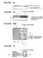
- an Eu 1 Ba 2 Cu 3 O 7-y thin film 2 having a thickness of 5 nanometers was deposited on the left half of the surface of a MgO (100) single crystal substrate 3 by a sputtering process.
- the conditions of the sputtering process were as follows: Temperature of substrate 630°C Sputtering gases Ar 8 sccm O 2 4 sccm Pressure 6,665 Pa (5 x 10 -2 Torr)
- the Eu 1 Ba 2 Cu 3 O 7-y thin film 2 was composed of a single crystal of which a -axes and b -axes shifted at angle of 45° to b -axes and c -axes of the lattices of the surface of the MgO substrate 3.
- a c -axis oriented Y 1 Ba 2 Cu 3 O 7-x oxide superconductor thin film 1 having a thickness of 300 nanometers were deposited on the Eu 1 Ba 2 Cu 3 O 7-y thin film 2 and the exposing right half of the surface of the MgO (100) single crystal substrate 3 by a sputtering process.
- the conditions of the sputtering process were as follows: Temperature of substrate 630°C Sputtering gases Ar 8 sccm O 2 4 sccm Pressure 6,665 Pa (5 x 10 -2 Torr)
- the c -axis oriented Y 1 Ba 2 Cu 3 O 7-x oxide superconductor thin film 1 grew epitaxially so as to conform its lattices to those of the Eu 1 Ba 2 Cu 3 O 7-y thin film 2 and MgO substrate 3.
- the Y 1 Ba 2 Cu 3 O 7-x oxide superconductor thin film 1 was etched by a reactive ion etching process so that the narrow portion 15 having a length of 10 ⁇ m and a width of 5 ⁇ m, on the center portion of which the grain boundary 4 was positioned, was created between portions 10 and 20 having a sufficient width.
- the width of the narrow portion 15 was not so narrow as that of a conventional Dayem bridge type Josephson device.
- the Josephson device as shown in Figure 1C was completed.
- the Josephson device manufactured by the method in accordance with the present invention was constituted of an oxide superconductor thin film which had a planar surface and a portion 15 having a narrow width between two portions 11 and 12 having a sufficient width.
- the lattice orientations of two portions 11 and 12 were different from each other so that the two portions 11 and 12 were weakly linked by the grain boundary 4 in the narrow portion 15, which constituted the superconducting barrier of the Josephson device.
- a current-voltage characteristics of the above mentioned Josephson device was measured at a temperature of 85K.
- a microwave of 15 GHz and of 0.2 mW was irradiated, clear Shapiro steps of was observed at multiple voltages of 31 ⁇ V, and therefore, it could be ascertained that the Josephson junction was realized in the device.
- the above mentioned Josephson device is manufactured in accordance with the above mentioned process, the limitation in the fine processing technique required for manufacturing the Josephson device is relaxed.
- the superconducting barrier is constituted of the grain boundary, it become easy to form the superconducting barrier sharply. Accordingly, it is easy to manufacture the Josephson device with good repeatability, and the manufactured Josephson device has a stable performance.
- FIG. 2 there is shown a diagrammatic plane view of one embodiment of the superconducting device in accordance with the present invention.
- the Josephson junction device shown in this embodiment is a dc SQUID.
- the dc SQUID includes a MgO (100) substrate 3, a Eu 1 Ba 2 Cu 3 O 7-y thin film 2 deposited on the left half of the surface of the MgO substrate 3 and an annular shaped c -axis oriented Y 1 Ba 2 Cu 3 O 7-x oxide superconductor thin film 1 formed on the MgO substrate 3 and the Eu 1 Ba 2 Cu 3 O 7-y thin film 2.
- the Y 1 Ba 2 Cu 3 O 7-x oxide superconductor thin film 1 is formed an annular ring shape of which two portions cross the step portion formed of the a Eu 1 Ba 2 Cu 3 O 7-y thin film 2.
- the Eu 1 Ba 2 Cu 3 O 7-y thin film 2 is composed of a single crystal of which a -axes and b -axes shifted at angle of 45° to b -axes and c -axes of the lattices of the surface of the MgO substrate 3.
- the Y 1 Ba 2 Cu 3 O 7-x oxide superconductor thin film 1 grows epitaxially so as to conform its lattices to those of the Eu 1 Ba 2 Cu 3 O 7-y thin film 2 and MgO substrate 3. Therefore, the a -axes and b -axes of lattices of a portion 20 of the Y 1 Ba 2 Cu 3 O 7-x oxide superconductor thin film 1, which is deposited on the Eu 1 Ba 2 Cu 3 O 7-y thin film 2 sift at angle 45° to those of a portion 10 of the Y 1 Ba 2 Cu 3 O 7-x oxide superconductor thin film 1, which is deposited on the surface 13 of the MgO substrate 3.
- Grain boundaries 4 and 14 are formed on the interfaces between the portions 10 and 20 of the Y 1 Ba 2 Cu 3 O 7-x oxide superconductor thin film 1 just on the step portion formed by the Eu 1 Ba 2 Cu 3 O 7-y thin film 2.
- the portions 10 and 20 of the Y 1 Ba 2 Cu 3 O 7-x oxide superconductor thin film 1 are linked weakly by the grain boundaries 4 and 14 which constituted the superconducting barriers of the Josephson junctions.
- the above mentioned dc SQUID was manufactured by the following method in accordance with the present invention. At first, an Eu 1 Ba 2 Cu 3 O 7-y thin film 2 was deposited on the left half of the MgO (100) substrate 3 by a sputtering process. The sputtering was performed under the same condition as that of the Embodiment 1.
- annular shaped Y 1 Ba 2 Cu 3 O 7-x oxide superconductor thin film 1 was deposited on the Eu 1 Ba 2 Cu 3 O 7-y thin film 2 and the exposing right half of the surface of the MgO (100) substrate 3 by a sputtering process in which patterned silicone plate was used as a mask.
- the above mentioned dc SQUID is manufactured in accordance with the above mentioned process, the limitation in the fine processing technique required for manufacturing the dc SQUID is relaxed.
- the superconducting barriers are constituted of the grain boundaries, it become easy to form sharp superconducting barriers of which properties are linear up. Accordingly, it is easy to manufacture the dc SQUID with good repeatability, and the manufactured dc SQUID has a stable performance.
Landscapes
- Engineering & Computer Science (AREA)
- Chemical & Material Sciences (AREA)
- Ceramic Engineering (AREA)
- Manufacturing & Machinery (AREA)
- Superconductor Devices And Manufacturing Methods Thereof (AREA)
Claims (12)
- Dispositif à jonction de Josephson comprenant un substrat (3) et un film mince d'oxyde supraconducteur formé par un oxyde de cuivre supraconducteur composite à température Tc élevée, formé sur une surface principale du substrat, qui comprend deux parties (11,12;10,20) constituées de monocristaux de l'oxyde supraconducteur, les réseaux de l'un de ces cristaux étant décalé d'un angle de 45° par rapport à ceux de l'autre cristal, et une limite de grain (4;4,14) entre lesdites parties, qui constitue une liaison faible de la jonction de Josephson, caractérisé en ce que le dispositif à jonction de Josephson comprend en outre un film mince d'oxyde (2) formé de Eu1Ba2Cu3O7-y, Gd1Ba2Cu3O7-y ou Sm1Ba2Cu3O7-v formé sur une partie de la surface principale du substrat, qui est constituée par un monocristal dont les réseaux sont décalés d'un angle de 45° par rapport à ceux de la surface principale du substrat, sur laquelle l'une desdites deux parties (12;20) du film mince d'oxyde supraconducteur est formée, tandis que l'autre partie (11;10) du film mince supraconducteur est formée directement sur la surface principale du substrat de telle sorte que les réseaux desdites deux parties du film mince d'oxyde supraconducteur sont respectivement alignés avec ceux du film mince d'oxyde, et la surface principale du substrat et la limite de grain (4;14), qui constitue une liaison faible de la jonction de Josephson, est formée précisément sur la partie étagée formée de film mince d'oxyde.
- Dispositif à jonction de Josephson selon la revendication 1, caractérisé en ce que le film mince d'oxyde (2) possède une épaisseur de 1 à 10 manomètres.
- Dispositif à jonction de Josephson selon la revendication 1 ou 2, caractérisé en ce que ledit film mince d'oxyde supraconducteur (1) comprend deux parties espacées entre lesdites deux parties (10,20), qui recoupent la partie étagée formée du film mince d'oxyde (2) de sorte que chacune des deux parties espacées incluent la limite de grain (4,14) qui constitue la liaison faible de la jonction de Josephson.
- Dispositif à jonction de Josephson selon la revendication 3, caractérisé en ce que ledit film mince d'oxyde supraconducteur (1) est agencé avec une forme annulaire de sorte que le dispositif à jonction de Josephson constitue un dispositif SQUID à courant continu.
- Dispositif à jonction de Josephson selon l'une quelconque des revendications 1 à 4, caractérisé en ce que la partie dudit film mince d'oxyde supraconducteur (1), qui recoupe la partie étagée formée dudit film mince d'oxyde (2) possède une largeur inférieure à celle d'autres parties dudit film mince d'oxyde supraconducteur (1).
- Dispositif à jonction de Josephson selon la revendication 5, caractérisé en ce que la partie étroite du film mince d'oxyde supraconducteur possède une largeur de 1,5 à 15 µm et une longueur de 5 à 50 µm.
- Dispositif à jonction de Josephson selon l'une quelconque des revendications 1 à 6, caractérisé en ce que ledit film mince d'oxyde supraconducteur (1) est formé d'un oxyde supraconducteur choisi dans le groupe comprenant un matériau supraconducteur constitué d'un oxyde composite du type Y-Ba-Cu-O, un matériau supraconducteur composite du tpye Bi-Sr-Ca-Cu-O, et un matériau supraconducteur formé d'un oxyde composite du type Tl-Ba-Ca-Cu-O.
- Dispositif à jonction de Josephson selon l'une quelconque des revendications 1 à 7, caractérisé en ce que le substrat est formé d'un matériau choisi dans le groupe comprenant un substrat en MgO (100), un substrat en SrTiO3 (110) et un substrat formé de zircone stabilisée par de l'yttrium (YSZ).
- Procédé pour fabriquer un dispositif à jonction de Josephson, comprenant les étapes consistant à former, sur une partie d'une surface principale d'un substrat (3), un film mince d'oxyde (2), qui est formé d'un monocristal de Eu1Ba2Cu3O6-y, Gd1Ba2Cu3O7-y ou Sm1Ba2Cu3O7-v, dont les réseaux sont décalés d'un angle de 45° par rapport aux réseaux de la surface du substrat, et former un film mince d'oxyde supraconducteur constitué d'un oxyde de cuivre supraconducteur composite à température Tc élevée sur le film d'oxyde mince et la surface principale exposée du substrat de telle sorte que le film mince d'oxyde supraconducteur croît de façon épitaxiale de manière à adapter ses réseaux à ceux du film d'oxyde mince et du substrat, et que les réseaux d'une partie du film mince d'oxyde supraconducteur, qui est déposé sur le film mince d'oxyde, sont décalés d'un angle de 45° par rapport à ceux des parties du film mince d'oxyde supraconducteur, qui est déposé sur la surface du substrat pour former une limite de grain (4;4,14) entre les deux parties du film mince d'oxyde supraconducteur précisément sur une partie étagée formée du film mince d'oxyde, qui constitue la liaison faible de la jonction de Josephson.
- Procédé selon la revendication 9, caractérisé en ce que le procédé comprend en outre une étape consistant à rétrécir une partie (15) du film mince d'oxyde supraconducteur, qui croise la partie étagée formée sur le film mince d'oxyde au moyen d'un procédé de corrosion ionique réactive.
- Procédé selon la revendication 9 ou 10, caractérisé en ce qu'on forme le film mince d'oxyde supraconducteur en utilisant un masque constitué d'une plaque de silicone de sorte que le film mince d'oxyde supraconducteur est conformé de manière à comporter deux parties espacées recoupant la partie étagée formée du film mince d'oxyde, dont chacune inclut la limite de grain qui constitue la liaison faible de la jonction de Josephson.
- Procédé selon la revendication 11, caractérisé en ce que le film mince d'oxyde supraconducteur est agencé avec une forme annulaire qui inclut deux parties recoupant la partie étagée formée du film mince d'oxyde et dont chacune inclut la limite de grain qui constitue la liaison faible de la jonction de Josephson.
Applications Claiming Priority (4)
| Application Number | Priority Date | Filing Date | Title |
|---|---|---|---|
| JP201220/91 | 1991-07-16 | ||
| JP20122191 | 1991-07-16 | ||
| JP20122091 | 1991-07-16 | ||
| JP201221/91 | 1991-07-16 |
Publications (2)
| Publication Number | Publication Date |
|---|---|
| EP0524862A1 EP0524862A1 (fr) | 1993-01-27 |
| EP0524862B1 true EP0524862B1 (fr) | 1996-12-18 |
Family
ID=26512666
Family Applications (1)
| Application Number | Title | Priority Date | Filing Date |
|---|---|---|---|
| EP92402057A Expired - Lifetime EP0524862B1 (fr) | 1991-07-16 | 1992-07-16 | Dispositif à jonction Josephson en oxyde supraconducteur et procédé pour sa fabrication |
Country Status (2)
| Country | Link |
|---|---|
| EP (1) | EP0524862B1 (fr) |
| DE (1) | DE69215993T2 (fr) |
Families Citing this family (5)
| Publication number | Priority date | Publication date | Assignee | Title |
|---|---|---|---|---|
| JPH05251771A (ja) * | 1991-12-02 | 1993-09-28 | Sumitomo Electric Ind Ltd | 人工粒界型ジョセフソン接合素子およびその作製方法 |
| CA2084264C (fr) * | 1991-12-02 | 1996-11-26 | Takao Nakamura | Cellule de memoire a effet josephson avec un materiau superconducteur oxyde et procede de preparation |
| EP0557207B1 (fr) * | 1992-02-19 | 2000-05-03 | Sumitomo Electric Industries, Ltd. | Dispositif à jonction de type Josephson à supraconducteur d'oxyde et procédé de préparation |
| US5593950A (en) * | 1992-07-28 | 1997-01-14 | Nippon Telegraph & Telephone Corporation | Lattice matching super conducting device with a- and c- axes |
| JPH0817250B2 (ja) * | 1993-07-30 | 1996-02-21 | 工業技術院長 | 異方性超伝導素子とその作製方法及びこれを用いたフラクソンデバイス |
Citations (1)
| Publication number | Priority date | Publication date | Assignee | Title |
|---|---|---|---|---|
| WO1992016974A1 (fr) * | 1991-03-19 | 1992-10-01 | Conductus, Inc. | Jonctions des peripheries de grains dans des films supraconducteurs a haute temperature |
Family Cites Families (2)
| Publication number | Priority date | Publication date | Assignee | Title |
|---|---|---|---|---|
| JPS59210677A (ja) * | 1983-05-14 | 1984-11-29 | Nippon Telegr & Teleph Corp <Ntt> | ジヨセフソン接合を用いた光検出素子 |
| CA1336567C (fr) * | 1988-02-03 | 1995-08-08 | Franz Joseph Himpsel | Epitaxie sur silicium de supraconducteurs a t- elevee |
-
1992
- 1992-07-16 DE DE69215993T patent/DE69215993T2/de not_active Expired - Fee Related
- 1992-07-16 EP EP92402057A patent/EP0524862B1/fr not_active Expired - Lifetime
Patent Citations (1)
| Publication number | Priority date | Publication date | Assignee | Title |
|---|---|---|---|---|
| WO1992016974A1 (fr) * | 1991-03-19 | 1992-10-01 | Conductus, Inc. | Jonctions des peripheries de grains dans des films supraconducteurs a haute temperature |
Also Published As
| Publication number | Publication date |
|---|---|
| EP0524862A1 (fr) | 1993-01-27 |
| DE69215993D1 (de) | 1997-01-30 |
| DE69215993T2 (de) | 1997-06-19 |
Similar Documents
| Publication | Publication Date | Title |
|---|---|---|
| US5729046A (en) | Superconducting device having pinning regions | |
| EP0567386A2 (fr) | Capteur de magnétisme planaire utilisant un interféromètre quantique à supraconducteur à oxyde | |
| EP0496259B1 (fr) | Dispositif microjonction à supraconducteur haute température utilisant une jonction bord à bord SNS en palier | |
| US5196395A (en) | Method for producing crystallographic boundary junctions in oxide superconducting thin films | |
| EP0467777B1 (fr) | Méthode pour la fabrication d'un dispositif en matériau supraconducteur et le dispositif supraconducteur fabriqué de cette manière | |
| US5439875A (en) | Process for preparing Josephson junction device having weak link of artificial grain boundary | |
| EP0572324B1 (fr) | Dispositif jonction de type Josephson à supraconducteur d'oxyde et procédé de sa préparation | |
| EP0446146B1 (fr) | Dispositif jonction Josephson empilé composé de matériau supraconducteur d'oxyde | |
| EP0573340B1 (fr) | Dispositif à jonction de type Josephson composé de supraconducteur d'oxyde | |
| CA2073831C (fr) | Dispositif a jonction de josephson oxyde-supraconducteur et sa methode de fabrication | |
| EP0524862B1 (fr) | Dispositif à jonction Josephson en oxyde supraconducteur et procédé pour sa fabrication | |
| EP0475838B1 (fr) | Dispositif supraconducteur avec un film supraconducteur de épaisseur réduite et methode pour sa fabrication | |
| CA2064169C (fr) | Procede pour l'obtention d'un compose d'oxyde supraconducteur en couche mince | |
| EP0546904B1 (fr) | Méthode pour fabriquer un dispositif à jonction artificielle de type Josephson à limite de grain | |
| US5612290A (en) | Josephson junction device formed of oxide superconductor | |
| EP0557207B1 (fr) | Dispositif à jonction de type Josephson à supraconducteur d'oxyde et procédé de préparation | |
| EP0545815B1 (fr) | Dispositif à jonction Josephson en oxyde supraconducteur et procédé pour sa fabrication | |
| US5721196A (en) | Stacked tunneling and stepped grain boundary Josephson junction | |
| EP0476687A2 (fr) | Structure d'adjonction supraconducteur et procédé pour sa fabrication | |
| EP0422641A2 (fr) | Dispositif supraconducteur | |
| EP0476617B1 (fr) | Structure de jonction supraconducteur et procédé pour sa fabrication | |
| EP0739045A1 (fr) | Dispositif supraconducteur à effet de champ à canal supraconducteur et procédé de fabrication | |
| EP0545777B1 (fr) | Méthode pour la fabrication d'un couche mince en matériau supraconducteur ayant un portion à épaisseur réduite de film supraconducteur et le dispositif supraconducteur utilisant ce film supraconducteur | |
| EP0790655B1 (fr) | Dispositif supraconducteur à effet de champ à canal supraconducteur et procédé de fabrication | |
| Linzen et al. | Application of silicon substrates for high-Tc Josephson junctions and SQUIDs |
Legal Events
| Date | Code | Title | Description |
|---|---|---|---|
| PUAI | Public reference made under article 153(3) epc to a published international application that has entered the european phase |
Free format text: ORIGINAL CODE: 0009012 |
|
| AK | Designated contracting states |
Kind code of ref document: A1 Designated state(s): DE FR GB NL |
|
| 17P | Request for examination filed |
Effective date: 19930701 |
|
| 17Q | First examination report despatched |
Effective date: 19941227 |
|
| GRAG | Despatch of communication of intention to grant |
Free format text: ORIGINAL CODE: EPIDOS AGRA |
|
| GRAH | Despatch of communication of intention to grant a patent |
Free format text: ORIGINAL CODE: EPIDOS IGRA |
|
| APBJ | Interlocutory revision of appeal recorded |
Free format text: ORIGINAL CODE: EPIDOS IRAPE |
|
| GRAH | Despatch of communication of intention to grant a patent |
Free format text: ORIGINAL CODE: EPIDOS IGRA |
|
| GRAA | (expected) grant |
Free format text: ORIGINAL CODE: 0009210 |
|
| AK | Designated contracting states |
Kind code of ref document: B1 Designated state(s): DE FR GB NL |
|
| REF | Corresponds to: |
Ref document number: 69215993 Country of ref document: DE Date of ref document: 19970130 |
|
| ET | Fr: translation filed | ||
| PLBE | No opposition filed within time limit |
Free format text: ORIGINAL CODE: 0009261 |
|
| STAA | Information on the status of an ep patent application or granted ep patent |
Free format text: STATUS: NO OPPOSITION FILED WITHIN TIME LIMIT |
|
| 26N | No opposition filed | ||
| REG | Reference to a national code |
Ref country code: GB Ref legal event code: IF02 |
|
| PGFP | Annual fee paid to national office [announced via postgrant information from national office to epo] |
Ref country code: FR Payment date: 20020709 Year of fee payment: 11 |
|
| PGFP | Annual fee paid to national office [announced via postgrant information from national office to epo] |
Ref country code: GB Payment date: 20020710 Year of fee payment: 11 |
|
| PGFP | Annual fee paid to national office [announced via postgrant information from national office to epo] |
Ref country code: DE Payment date: 20020724 Year of fee payment: 11 |
|
| PGFP | Annual fee paid to national office [announced via postgrant information from national office to epo] |
Ref country code: NL Payment date: 20020730 Year of fee payment: 11 |
|
| PG25 | Lapsed in a contracting state [announced via postgrant information from national office to epo] |
Ref country code: GB Free format text: LAPSE BECAUSE OF NON-PAYMENT OF DUE FEES Effective date: 20030716 |
|
| PG25 | Lapsed in a contracting state [announced via postgrant information from national office to epo] |
Ref country code: NL Free format text: LAPSE BECAUSE OF NON-PAYMENT OF DUE FEES Effective date: 20040201 |
|
| PG25 | Lapsed in a contracting state [announced via postgrant information from national office to epo] |
Ref country code: DE Free format text: LAPSE BECAUSE OF NON-PAYMENT OF DUE FEES Effective date: 20040203 |
|
| GBPC | Gb: european patent ceased through non-payment of renewal fee |
Effective date: 20030716 |
|
| PG25 | Lapsed in a contracting state [announced via postgrant information from national office to epo] |
Ref country code: FR Free format text: LAPSE BECAUSE OF NON-PAYMENT OF DUE FEES Effective date: 20040331 |
|
| NLV4 | Nl: lapsed or anulled due to non-payment of the annual fee |
Effective date: 20040201 |
|
| REG | Reference to a national code |
Ref country code: FR Ref legal event code: ST |