EP0522356B1 - Method for detecting structural defect of film - Google Patents
Method for detecting structural defect of film Download PDFInfo
- Publication number
- EP0522356B1 EP0522356B1 EP92110633A EP92110633A EP0522356B1 EP 0522356 B1 EP0522356 B1 EP 0522356B1 EP 92110633 A EP92110633 A EP 92110633A EP 92110633 A EP92110633 A EP 92110633A EP 0522356 B1 EP0522356 B1 EP 0522356B1
- Authority
- EP
- European Patent Office
- Prior art keywords
- film
- thin film
- substrate
- light
- organic thin
- Prior art date
- Legal status (The legal status is an assumption and is not a legal conclusion. Google has not performed a legal analysis and makes no representation as to the accuracy of the status listed.)
- Expired - Lifetime
Links
- 238000000034 method Methods 0.000 title claims abstract description 23
- 230000007847 structural defect Effects 0.000 title description 20
- 239000010409 thin film Substances 0.000 claims abstract description 52
- 239000010408 film Substances 0.000 claims abstract description 42
- 230000007547 defect Effects 0.000 claims abstract description 28
- 239000000758 substrate Substances 0.000 claims abstract description 21
- 230000004907 flux Effects 0.000 claims abstract description 13
- 230000003287 optical effect Effects 0.000 description 11
- 238000011156 evaluation Methods 0.000 description 7
- 238000001514 detection method Methods 0.000 description 6
- 235000014113 dietary fatty acids Nutrition 0.000 description 4
- 229930195729 fatty acid Natural products 0.000 description 4
- 239000000194 fatty acid Substances 0.000 description 4
- 150000004665 fatty acids Chemical class 0.000 description 4
- 238000012545 processing Methods 0.000 description 4
- 238000012360 testing method Methods 0.000 description 4
- 238000004458 analytical method Methods 0.000 description 3
- 230000008859 change Effects 0.000 description 3
- 238000003384 imaging method Methods 0.000 description 3
- 239000012212 insulator Substances 0.000 description 3
- 238000005259 measurement Methods 0.000 description 3
- 239000002184 metal Substances 0.000 description 3
- 229910052751 metal Inorganic materials 0.000 description 3
- 239000002245 particle Substances 0.000 description 3
- 238000010276 construction Methods 0.000 description 2
- 238000001493 electron microscopy Methods 0.000 description 2
- 238000010191 image analysis Methods 0.000 description 2
- 238000011835 investigation Methods 0.000 description 2
- 239000011368 organic material Substances 0.000 description 2
- 230000035945 sensitivity Effects 0.000 description 2
- 239000007787 solid Substances 0.000 description 2
- RYGMFSIKBFXOCR-UHFFFAOYSA-N Copper Chemical compound [Cu] RYGMFSIKBFXOCR-UHFFFAOYSA-N 0.000 description 1
- 241000519995 Stachys sylvatica Species 0.000 description 1
- 230000001464 adherent effect Effects 0.000 description 1
- 230000032683 aging Effects 0.000 description 1
- 230000015572 biosynthetic process Effects 0.000 description 1
- 239000012141 concentrate Substances 0.000 description 1
- 229910052802 copper Inorganic materials 0.000 description 1
- 239000010949 copper Substances 0.000 description 1
- 230000006866 deterioration Effects 0.000 description 1
- 238000011161 development Methods 0.000 description 1
- 230000018109 developmental process Effects 0.000 description 1
- 230000006872 improvement Effects 0.000 description 1
- 238000003475 lamination Methods 0.000 description 1
- 239000004973 liquid crystal related substance Substances 0.000 description 1
- 239000000463 material Substances 0.000 description 1
- 238000005442 molecular electronic Methods 0.000 description 1
- 150000002894 organic compounds Chemical class 0.000 description 1
- 239000002985 plastic film Substances 0.000 description 1
- 229920006255 plastic film Polymers 0.000 description 1
- 230000008569 process Effects 0.000 description 1
- 239000004065 semiconductor Substances 0.000 description 1
- 238000012800 visualization Methods 0.000 description 1
Images


Classifications
-
- G—PHYSICS
- G01—MEASURING; TESTING
- G01N—INVESTIGATING OR ANALYSING MATERIALS BY DETERMINING THEIR CHEMICAL OR PHYSICAL PROPERTIES
- G01N21/00—Investigating or analysing materials by the use of optical means, i.e. using sub-millimetre waves, infrared, visible or ultraviolet light
- G01N21/84—Systems specially adapted for particular applications
- G01N21/8422—Investigating thin films, e.g. matrix isolation method
-
- G—PHYSICS
- G01—MEASURING; TESTING
- G01N—INVESTIGATING OR ANALYSING MATERIALS BY DETERMINING THEIR CHEMICAL OR PHYSICAL PROPERTIES
- G01N21/00—Investigating or analysing materials by the use of optical means, i.e. using sub-millimetre waves, infrared, visible or ultraviolet light
- G01N21/84—Systems specially adapted for particular applications
- G01N21/88—Investigating the presence of flaws or contamination
Definitions
- the present invention relates to a use of a method for detecting imperfections of thin film formed on a substrate.
- An LB film is constituted of a regular lamination of monomolecular layers of an organic compound.
- the LB film has enabled formation of a uniform ultra-thin film by controlling the film thickness thereof in the order of the unit of a molecular length, that is in the order of magnitude of nm (nanometer, 10 -9 m). Many attempts have been made to use the LB film as an insulator.
- the examples of the attempts include a tunnel junction element having a structure of metal/insulator/metal (MIM) [G.L. Larkins, et al.: “Thin Solid Films", Vol. 99 (1983)]; a light-emitting element having a structure of metal/insulator/semiconductor (MIS) [G.C. Roberts, et al.: Electronics Letters, Vol. 20, p. 489 (1984)]; and a switching element [N.J. Thomas, et al.: Electronics Letters, Vol. 20, p. 838 (1984)].
- MIM metal/insulator/metal
- MIS metal/insulator/semiconductor
- the structural defect of the LB film is required to be visualized and to be numerically evaluated within a limited time.
- the evaluation by electron microscopy is complicated for the evaluation of structural defects of an LB film because many parameters have to be controlled to obtain significant results. Therefore, the electron microscopy requires technical skill as well as much time for the measurement.
- the US-A-4 966 457 discloses a method that requires two light beams of different wavelength to detect particles adherent to a thin film, as for instance reticles and pellicles. These films are several ⁇ m thick, typically 3 to 10 wavelengths and the incident angle of the two light beams is varied for detecting the particles.
- the JP-A-0 118 5934 discloses a method of detecting a foreign body on a periodically structured surface with known structure.
- the setup is done in a way that the image of a proper, clean object is cancelled out at the point of observation and only particles or defects, that are not part of the desired pattern, result in a high contrast image.
- a method is described using physical contact between a light guide and a film covered substrate, like a soft plastic film on paper, to detect defects, namely non coated areas in the film.
- This known method is not suited for sensitive films because those films will be destructed thereby.
- For the thin films, to which this known method is directed, are very thick compared to the films in question, as for instance Langmuir-Blodgett films.
- Fig. 1 illustrates schematically the principle of the detection of defects in the structure of a thin film in the present invention.
- Fig. 2 illustrates schematically a apparatus for detecting a defect in the structure of an organic thin film by the method of the present invention.
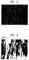
- Fig. 3 is an photographic image of defects of a fatty acid LB film obtained by use of an apparatus employing the method of the present invention.
- Fig. 4 is a polarizing microscopic image of the same part of a fatty acid LB film as in Fig.3.
- Fig. 5 illustrates schematically the principle of the detection of the structure at and around an interface of a thin film in the present invention.
- Fig. 1 illustrates schematically the principle of the detection of defects in structure of a thin film in the present invention.
- a flat thin film 1 in the drawing is made of an organic material.
- the organic thin film as the object of the present invention has generally a thickness of from several ten ⁇ to several thousand ⁇ . In particular in the case where the thin film is an LB film, the thickness is in the range of from several ⁇ to thousand ⁇ , preferably from 4 ⁇ to 1000 ⁇ , more preferably from 50 ⁇ to 100 ⁇ as the object of-evaluation of the film. Minute defects 1a like pinholes inside the organic thin film are also shown schematically in Fig. 1.
- a specimen 16 is constituted of a flat substrate 2 and an organic thin film 1 formed thereon.
- a light flux (a projected light) L is projected from a light source (not shown in the drawing) such as a laser source to the substrate 2 in a direction nearly parallel to the substrate 2. If the organic thin film 1 is uniform and has no defect in the internal structure the introduced light flux L is simply reflected by the organic thin film 1, or transmitted through the thin film 1 and then reflected by the substrate 2, thus the reflected light is ejected from the other end.
- the organic thin film involves a defect 1a like a pinhole inside
- the light flux L introduced to the defect 1a is scattered by the defect 1a. That is, the light flux L is scattered by the change of the refractive index resulting from the defect 1a, and the scattered light is ejected in various directions.
- the scattered light 17 directed precisely or nearly perpendicular to the substrate 2 is collected by a condensor lens (or an objective) 8, and an image of the thin film structure of the organic thin film 1 caused by the scattered light 17 is formed on a plane of an imaging means such as a CCD (not shown in the drawing).
- the light flux L is projected in a direction parallel or nearly parallel to the organic thin film 1, whereby the light which is transmitted simply through the thin film 1 and the regular reflection light 18 which is reflected regularly by the substrate 2 is not introduced to the condensor lens 8.
- the image of the scattered light caused by defects in the thin film structure and formed by an imaging means is subjected to image analysis with an image-processing means (not shown in the drawing), thereby the structural defects in organic thin films being detected.
- Fig. 2 illustrates schematically an apparatus for detecting a defect in structure of an organic thin film by the method of the present invention.
- an optical microscope system is applied to the present invention.
- the construction of this example does not interfere with the normal use of the optical microscope system such as a light source for observation, a polarizer plate, an analyzer plate, a camera, and so forth.
- the flat organic thin film 1 is formed on an optically flat substrate 2.
- a support 3 is constructed of an XYZ three-axis stage which is movable in an XY plane and in a Z axis direction.
- a substrate 2 having an organic thin film 1 is placed on the support.
- a light source means 4 comprises an LED or a laser source.
- a light-projecting means 5 converges the light flux from the light source means 4, and projects the light as fine flux to the organic thin film 1 in a direction parallel or nearly parallel to the substrate 2.
- the light source means 4 and the light-projecting means 5 are integrated into one body, and are provided with a position control device for projecting light flux in a direction nearly parallel to the organic thin film.
- the light source means 4 and the light-projecting means 5 are constructed in one body, for example, so as to be rotatable around the centor of the support 3.
- a photosensor 6 monitors the variation of light output from the light source means 4 by detecting the light flux having passed through the organic thin film 1, or the light flux of both having passed through the organic thin film and having been regularly reflected by the substrate 2.
- the light output from the light source means 4 is stabilized by inputting the output signal from the photosensor 6 to the stabilized power source 7.
- image information obtained by an optical area sensor 10, which is an imaging means described later, is standardized to facilitate comparison of organic thin films to be tested.
- An objective 8 concentrates the scattered light caused by a structural defect in a direction perpendicular or nearly perpendicular to the organic thin film 1, and introduces the light through a half mirror 9 to an optical area sensor 10 at a predetermined magnification to form image information thereon regarding the structural defects of the organic thin film 1.
- an image is formed as a bright spot caused by scattered light from the defect in the organic thin film 1 as shown in drawings shown later.
- the optical area sensor 10 converts image information regarding the organic thin film 1 into an electric image data.
- the sensitivity of the optical area sensor 10 is optimized by an optimizing circuit 15 so as to carry out digital treatment effectively.
- the image data from the optical area sensor 10 is digitalized by an A/D converter 11, and is inputted to an image-processing means 12.
- the image signal, after being processed by the image-processing means 12, is inputted to a computer 13.
- the computer 13 analyses the image signal from the image-processing means 12, thereby characterizing the structural defect of the organic thin film 1.
- the computer 13 controls the movement of the support 3 three-dimensionally (in XYZ directions), thereby enabling automatic observation such as automatic focusing, and automatic positional measurement of density of structural defects.
- the state of the structural defects is observed by utilizing the scattered light, which is caused by structural defects of the organic thin film 1, through the objective 8 and the half mirror 9.
- Fig. 3 is a photographic image of defects in a fatty acid LB film obtained by use of an apparatus employing the method of the present invention.
- Fig. 4 is a polarizing microscopic image of the same fatty acid LB film taken by means of a conventional optical microscope, for reference.
- the white spots show structural defects such as pinholes.
- the present invention enables clear detection of structural defects of an organic thin film as shown in Fig. 3, and allows detection of structural defect and evaluation of an organic thin film with high accuracy in comparison with the photograph obtained with a conventional optical microscope as shown in Fig. 4.
- Fig. 5 illustrates another evaluation method employing a method of detecting defects at the interface of a thin film with a second material with higher refractive index.
- a first medium 19 has a higher refractive index than a second medium 20, the film under investigation.
- the light flux that is introduced at an angle of incidence corresponding to the critical angle or smaller which depends on the refractive indexes of the both mediums 19 and 20 is totally reflected at the interface 19/20 without leaking into the film 20 more than a small fraction of the wavelength. If the refractive index changes at or around the interface, the light is not totally reflected at the interface any more but is scattered by the imperfection. Accordingly, in the same manner as described by reference to Fig.
- the present invention provides a method for detecting a structural defect such as a film-lacking portion (like a pinhole) in a simple manner.
- the method of the present invention is applicable not only to a defect which pierces through a film like the defect la at the left side in Fig. 1, but also to a defect which is localized near an interface like the defect la at the right side of Fig. 1.
- the present invention enables visualization of a structural defect of an organic thin film (structural change which causes change of refractive index to incident light) in a simple manner as with a conventional optical microscope in the air. Further the present invention enables image analysis to analyse a density of defect and the distribution thereof, a size of defect and the distribution thereof, further a correlation of a distribution of defect with that of domain, and so forth.
- the present invention provides a method for testing and evaluating the quality of a thin film structure, especially of an organic thin film quickly with high precision in a simple manner in the air by setting the elements as described above.
- the present invention also provides a method for testing the interfacial structure of a thin film.
- the testing method and the testing apparatus of the present invention are applicable widely to evaluation of the state of a film, such as an LB film and a liquid crystal film or similar organic films with molecular dimensions.
Landscapes
- Physics & Mathematics (AREA)
- General Physics & Mathematics (AREA)
- Pathology (AREA)
- Life Sciences & Earth Sciences (AREA)
- Chemical & Material Sciences (AREA)
- Analytical Chemistry (AREA)
- Biochemistry (AREA)
- Health & Medical Sciences (AREA)
- Immunology (AREA)
- General Health & Medical Sciences (AREA)
- Mathematical Physics (AREA)
- Investigating Materials By The Use Of Optical Means Adapted For Particular Applications (AREA)
- Investigating Or Analyzing Materials By The Use Of Electric Means (AREA)
- Testing Or Measuring Of Semiconductors Or The Like (AREA)
- Image Processing (AREA)
- Image Analysis (AREA)
Abstract
Description
Claims (5)
- Use of a method for detecting imperfections of a thin film formed on a substrate, said method comprisingto detect defects in the film structure of an organic thin film (1, 20) on top of a substrate (2), said film having a thickness in the range of from several 0.1 nm to 100 nm.projecting a visible light flux in a direction nearly parallel to the face of the substrate,separating light reflected from the thin film and the substrate from a light scattered in a direction perpendicular or nearly perpendicular to the face of the substrate, andreading information only of the scattered light,
- The use according to claim 1, whereinthe thickness of said film is in the range of from 0.4 nm to 100 nm.
- The use according to claim 2, whereinthe thickness of said film is in the range of from 5nm to 100 nm.
- The use according to claim 1, 2 or 3, whereinthe film (20) is a Langmuir-Blodgett film (20).
- The use according to claim 4, whereinthe Langmuir-Blodgett film (20) is covered by a second film (19) having a higher refractive index than the Langmuir-Blodgett film.
Applications Claiming Priority (2)
| Application Number | Priority Date | Filing Date | Title |
|---|---|---|---|
| JP3178686A JP3013519B2 (en) | 1991-06-24 | 1991-06-24 | Inspection method and inspection device for thin film structure |
| JP178686/91 | 1991-06-24 |
Publications (3)
| Publication Number | Publication Date |
|---|---|
| EP0522356A2 EP0522356A2 (en) | 1993-01-13 |
| EP0522356A3 EP0522356A3 (en) | 1993-06-30 |
| EP0522356B1 true EP0522356B1 (en) | 1998-09-09 |
Family
ID=16052779
Family Applications (1)
| Application Number | Title | Priority Date | Filing Date |
|---|---|---|---|
| EP92110633A Expired - Lifetime EP0522356B1 (en) | 1991-06-24 | 1992-06-24 | Method for detecting structural defect of film |
Country Status (5)
| Country | Link |
|---|---|
| US (1) | US5305079A (en) |
| EP (1) | EP0522356B1 (en) |
| JP (1) | JP3013519B2 (en) |
| AT (1) | ATE170978T1 (en) |
| DE (1) | DE69226911T2 (en) |
Families Citing this family (7)
| Publication number | Priority date | Publication date | Assignee | Title |
|---|---|---|---|---|
| US5625722A (en) * | 1994-12-21 | 1997-04-29 | Lucent Technologies Inc. | Method and apparatus for generating data encoded pulses in return-to-zero format |
| DE19716264C2 (en) | 1997-04-18 | 2002-07-25 | Fraunhofer Ges Forschung | Device and method for checking a surface of an object |
| US6166366A (en) * | 1997-07-23 | 2000-12-26 | Cc1, Inc. | System and method for monitoring and controlling the deposition of pattern and overall material coatings |
| JP2001004347A (en) * | 1999-06-22 | 2001-01-12 | Mitsubishi Electric Corp | Defect inspection equipment |
| JP2006041352A (en) * | 2004-07-29 | 2006-02-09 | Dainippon Screen Mfg Co Ltd | Coat inspection device, inspection system, program, coat inspection method and inspection method of printed circuit board |
| JP2010032265A (en) * | 2008-07-25 | 2010-02-12 | Canon Inc | Inspection device of foreign matter, exposure system and device manufacturing method |
| CN105738379B (en) * | 2014-12-12 | 2018-10-19 | 上海和辉光电有限公司 | A kind of detection device and detection method of polysilicon membrane |
Family Cites Families (10)
| Publication number | Priority date | Publication date | Assignee | Title |
|---|---|---|---|---|
| US3782836A (en) * | 1971-11-11 | 1974-01-01 | Texas Instruments Inc | Surface irregularity analyzing method |
| US4297032A (en) * | 1980-02-14 | 1981-10-27 | The United States Of America As Represented By The Secretary Of The Navy | Dark field surface inspection illumination technique |
| JPS57132044A (en) * | 1981-02-10 | 1982-08-16 | Hitachi Metals Ltd | Discriminating method of surface defect |
| US4456374A (en) * | 1981-12-11 | 1984-06-26 | Johnson & Johnson | Detecting the presence or absence of a coating on a substrate |
| US4469442A (en) * | 1982-01-11 | 1984-09-04 | Japan Crown Cork Co., Ltd. | Detecting irregularities in a coating on a substrate |
| US4679938A (en) * | 1985-06-03 | 1987-07-14 | International Business Machines Corporation | Defect detection in films on ceramic substrates |
| JPH0820371B2 (en) * | 1988-01-21 | 1996-03-04 | 株式会社ニコン | Defect inspection device and defect inspection method |
| JPH01185934A (en) * | 1988-01-21 | 1989-07-25 | Hitachi Ltd | Foreign matter detection device for thin film transistor substrates |
| US4966455A (en) * | 1988-12-05 | 1990-10-30 | Union Camp Corporation | Real time mottle measuring device and method |
| JPH04132942A (en) * | 1990-09-25 | 1992-05-07 | Rikagaku Kenkyusho | Light scattering tomography method |
-
1991
- 1991-06-24 JP JP3178686A patent/JP3013519B2/en not_active Expired - Fee Related
-
1992
- 1992-06-19 US US07/901,160 patent/US5305079A/en not_active Expired - Lifetime
- 1992-06-24 AT AT92110633T patent/ATE170978T1/en active
- 1992-06-24 EP EP92110633A patent/EP0522356B1/en not_active Expired - Lifetime
- 1992-06-24 DE DE69226911T patent/DE69226911T2/en not_active Expired - Fee Related
Also Published As
| Publication number | Publication date |
|---|---|
| JP3013519B2 (en) | 2000-02-28 |
| EP0522356A2 (en) | 1993-01-13 |
| EP0522356A3 (en) | 1993-06-30 |
| ATE170978T1 (en) | 1998-09-15 |
| US5305079A (en) | 1994-04-19 |
| DE69226911T2 (en) | 1999-01-28 |
| DE69226911D1 (en) | 1998-10-15 |
| JPH051997A (en) | 1993-01-08 |
Similar Documents
| Publication | Publication Date | Title |
|---|---|---|
| EP0633450B1 (en) | Scanning probe microscope | |
| JP3258385B2 (en) | Optical board inspection system | |
| JP4500641B2 (en) | Defect inspection method and apparatus | |
| US7724360B2 (en) | Method and apparatus for inspecting foreign particle defects | |
| US20020135755A1 (en) | Scanning probe microscope assembly | |
| US5859364A (en) | Scanning probe microscope | |
| WO1992009880A2 (en) | Method and apparatus for automatic optical inspection | |
| JPH04337403A (en) | Photointegration type displacement sensor | |
| JPS63193005A (en) | Device for inspecting surface | |
| CN1662811A (en) | Two-spot phase-sensitive detection | |
| US5305079A (en) | Nondestructive method for detecting defects in thin film using scattered light | |
| JP3196945B2 (en) | Scanning optical microscope | |
| US5894349A (en) | Manufacturing method including near-field optical microscopic examination of a semiconductor substrate | |
| KR0126250B1 (en) | Micro gap width measuring method | |
| WO2003060589A1 (en) | Auto focussing device and method | |
| JP3523754B2 (en) | Scanning probe microscope | |
| KR102622581B1 (en) | Optical Critical Dimension metrology apparatus equipped with microspot spectroscopic ellipsometer | |
| JP2010038868A (en) | Optical viscosity measuring system | |
| JPH07167793A (en) | Phase difference semiconductor inspection device and method of manufacturing semiconductor device | |
| JPH1151616A (en) | Defect inspection equipment | |
| Knollenberg | A polarization diversity surface analysis system | |
| JPH10293103A (en) | Optical measuring method and apparatus and optical measuring apparatus for patterned substrate | |
| Talim | The measurement of refractive index in the visible and infrared at NPL | |
| Takahashi et al. | PATTERNED WAFER DEFECTS INSPECTION BY LASER SCATTERING IMAGE | |
| JPH02157608A (en) | Focusing method |
Legal Events
| Date | Code | Title | Description |
|---|---|---|---|
| PUAI | Public reference made under article 153(3) epc to a published international application that has entered the european phase |
Free format text: ORIGINAL CODE: 0009012 |
|
| AK | Designated contracting states |
Kind code of ref document: A2 Designated state(s): AT BE CH DE DK ES FR GB GR IT LI LU NL PT SE |
|
| PUAL | Search report despatched |
Free format text: ORIGINAL CODE: 0009013 |
|
| AK | Designated contracting states |
Kind code of ref document: A3 Designated state(s): AT BE CH DE DK ES FR GB GR IT LI LU NL PT SE |
|
| 17P | Request for examination filed |
Effective date: 19931112 |
|
| 17Q | First examination report despatched |
Effective date: 19951222 |
|
| GRAG | Despatch of communication of intention to grant |
Free format text: ORIGINAL CODE: EPIDOS AGRA |
|
| GRAG | Despatch of communication of intention to grant |
Free format text: ORIGINAL CODE: EPIDOS AGRA |
|
| GRAH | Despatch of communication of intention to grant a patent |
Free format text: ORIGINAL CODE: EPIDOS IGRA |
|
| GRAH | Despatch of communication of intention to grant a patent |
Free format text: ORIGINAL CODE: EPIDOS IGRA |
|
| GRAA | (expected) grant |
Free format text: ORIGINAL CODE: 0009210 |
|
| AK | Designated contracting states |
Kind code of ref document: B1 Designated state(s): AT BE CH DE DK ES FR GB GR IT LI LU NL PT SE |
|
| PG25 | Lapsed in a contracting state [announced via postgrant information from national office to epo] |
Ref country code: BE Free format text: LAPSE BECAUSE OF FAILURE TO SUBMIT A TRANSLATION OF THE DESCRIPTION OR TO PAY THE FEE WITHIN THE PRESCRIBED TIME-LIMIT Effective date: 19980909 Ref country code: IT Free format text: LAPSE BECAUSE OF FAILURE TO SUBMIT A TRANSLATION OF THE DESCRIPTION OR TO PAY THE FEE WITHIN THE PRE;WARNING: LAPSES OF ITALIAN PATENTS WITH EFFECTIVE DATE BEFORE 2007 MAY HAVE OCCURRED AT ANY TIME BEFORE 2007. THE CORRECT EFFECTIVE DATE MAY BE DIFFERENT FROM THE ONE RECORDED.SCRIBED TIME-LIMIT Effective date: 19980909 Ref country code: GR Free format text: LAPSE BECAUSE OF NON-PAYMENT OF DUE FEES Effective date: 19980909 Ref country code: NL Free format text: LAPSE BECAUSE OF FAILURE TO SUBMIT A TRANSLATION OF THE DESCRIPTION OR TO PAY THE FEE WITHIN THE PRESCRIBED TIME-LIMIT Effective date: 19980909 Ref country code: CH Free format text: LAPSE BECAUSE OF FAILURE TO SUBMIT A TRANSLATION OF THE DESCRIPTION OR TO PAY THE FEE WITHIN THE PRESCRIBED TIME-LIMIT Effective date: 19980909 Ref country code: ES Free format text: THE PATENT HAS BEEN ANNULLED BY A DECISION OF A NATIONAL AUTHORITY Effective date: 19980909 Ref country code: AT Free format text: LAPSE BECAUSE OF FAILURE TO SUBMIT A TRANSLATION OF THE DESCRIPTION OR TO PAY THE FEE WITHIN THE PRESCRIBED TIME-LIMIT Effective date: 19980909 Ref country code: LI Free format text: LAPSE BECAUSE OF FAILURE TO SUBMIT A TRANSLATION OF THE DESCRIPTION OR TO PAY THE FEE WITHIN THE PRESCRIBED TIME-LIMIT Effective date: 19980909 |
|
| REF | Corresponds to: |
Ref document number: 170978 Country of ref document: AT Date of ref document: 19980915 Kind code of ref document: T |
|
| REG | Reference to a national code |
Ref country code: CH Ref legal event code: EP |
|
| REF | Corresponds to: |
Ref document number: 69226911 Country of ref document: DE Date of ref document: 19981015 |
|
| ET | Fr: translation filed | ||
| PG25 | Lapsed in a contracting state [announced via postgrant information from national office to epo] |
Ref country code: SE Free format text: LAPSE BECAUSE OF FAILURE TO SUBMIT A TRANSLATION OF THE DESCRIPTION OR TO PAY THE FEE WITHIN THE PRESCRIBED TIME-LIMIT Effective date: 19981209 Ref country code: DK Free format text: LAPSE BECAUSE OF FAILURE TO SUBMIT A TRANSLATION OF THE DESCRIPTION OR TO PAY THE FEE WITHIN THE PRESCRIBED TIME-LIMIT Effective date: 19981209 |
|
| PG25 | Lapsed in a contracting state [announced via postgrant information from national office to epo] |
Ref country code: PT Free format text: LAPSE BECAUSE OF FAILURE TO SUBMIT A TRANSLATION OF THE DESCRIPTION OR TO PAY THE FEE WITHIN THE PRESCRIBED TIME-LIMIT Effective date: 19981211 |
|
| NLV1 | Nl: lapsed or annulled due to failure to fulfill the requirements of art. 29p and 29m of the patents act | ||
| REG | Reference to a national code |
Ref country code: CH Ref legal event code: PL |
|
| PG25 | Lapsed in a contracting state [announced via postgrant information from national office to epo] |
Ref country code: LU Free format text: LAPSE BECAUSE OF NON-PAYMENT OF DUE FEES Effective date: 19990624 |
|
| PLBE | No opposition filed within time limit |
Free format text: ORIGINAL CODE: 0009261 |
|
| STAA | Information on the status of an ep patent application or granted ep patent |
Free format text: STATUS: NO OPPOSITION FILED WITHIN TIME LIMIT |
|
| 26N | No opposition filed | ||
| REG | Reference to a national code |
Ref country code: GB Ref legal event code: IF02 |
|
| PGFP | Annual fee paid to national office [announced via postgrant information from national office to epo] |
Ref country code: FR Payment date: 20050608 Year of fee payment: 14 |
|
| PGFP | Annual fee paid to national office [announced via postgrant information from national office to epo] |
Ref country code: DE Payment date: 20050616 Year of fee payment: 14 |
|
| PGFP | Annual fee paid to national office [announced via postgrant information from national office to epo] |
Ref country code: GB Payment date: 20050622 Year of fee payment: 14 |
|
| PG25 | Lapsed in a contracting state [announced via postgrant information from national office to epo] |
Ref country code: GB Free format text: LAPSE BECAUSE OF NON-PAYMENT OF DUE FEES Effective date: 20060624 |
|
| PG25 | Lapsed in a contracting state [announced via postgrant information from national office to epo] |
Ref country code: DE Free format text: LAPSE BECAUSE OF NON-PAYMENT OF DUE FEES Effective date: 20070103 |
|
| GBPC | Gb: european patent ceased through non-payment of renewal fee |
Effective date: 20060624 |
|
| REG | Reference to a national code |
Ref country code: FR Ref legal event code: ST Effective date: 20070228 |
|
| PG25 | Lapsed in a contracting state [announced via postgrant information from national office to epo] |
Ref country code: FR Free format text: LAPSE BECAUSE OF NON-PAYMENT OF DUE FEES Effective date: 20060630 |