EP0518362A1 - Dispositif d'affichage d'image utilisant un télé-projecteur à crystaux liquides et réseau d'éléments optiques coniques utilisés dans un tel dispositif - Google Patents
Dispositif d'affichage d'image utilisant un télé-projecteur à crystaux liquides et réseau d'éléments optiques coniques utilisés dans un tel dispositif Download PDFInfo
- Publication number
- EP0518362A1 EP0518362A1 EP92109929A EP92109929A EP0518362A1 EP 0518362 A1 EP0518362 A1 EP 0518362A1 EP 92109929 A EP92109929 A EP 92109929A EP 92109929 A EP92109929 A EP 92109929A EP 0518362 A1 EP0518362 A1 EP 0518362A1
- Authority
- EP
- European Patent Office
- Prior art keywords
- light
- liquid
- aperture
- condensing
- crystal
- Prior art date
- Legal status (The legal status is an assumption and is not a legal conclusion. Google has not performed a legal analysis and makes no representation as to the accuracy of the status listed.)
- Granted
Links
Images


Classifications
-
- G—PHYSICS
- G02—OPTICS
- G02F—OPTICAL DEVICES OR ARRANGEMENTS FOR THE CONTROL OF LIGHT BY MODIFICATION OF THE OPTICAL PROPERTIES OF THE MEDIA OF THE ELEMENTS INVOLVED THEREIN; NON-LINEAR OPTICS; FREQUENCY-CHANGING OF LIGHT; OPTICAL LOGIC ELEMENTS; OPTICAL ANALOGUE/DIGITAL CONVERTERS
- G02F1/00—Devices or arrangements for the control of the intensity, colour, phase, polarisation or direction of light arriving from an independent light source, e.g. switching, gating or modulating; Non-linear optics
- G02F1/01—Devices or arrangements for the control of the intensity, colour, phase, polarisation or direction of light arriving from an independent light source, e.g. switching, gating or modulating; Non-linear optics for the control of the intensity, phase, polarisation or colour
- G02F1/13—Devices or arrangements for the control of the intensity, colour, phase, polarisation or direction of light arriving from an independent light source, e.g. switching, gating or modulating; Non-linear optics for the control of the intensity, phase, polarisation or colour based on liquid crystals, e.g. single liquid crystal display cells
- G02F1/133—Constructional arrangements; Operation of liquid crystal cells; Circuit arrangements
- G02F1/1333—Constructional arrangements; Manufacturing methods
- G02F1/1335—Structural association of cells with optical devices, e.g. polarisers or reflectors
- G02F1/133526—Lenses, e.g. microlenses or Fresnel lenses
-
- G—PHYSICS
- G02—OPTICS
- G02B—OPTICAL ELEMENTS, SYSTEMS OR APPARATUS
- G02B6/00—Light guides; Structural details of arrangements comprising light guides and other optical elements, e.g. couplings
- G02B6/04—Light guides; Structural details of arrangements comprising light guides and other optical elements, e.g. couplings formed by bundles of fibres
- G02B6/06—Light guides; Structural details of arrangements comprising light guides and other optical elements, e.g. couplings formed by bundles of fibres the relative position of the fibres being the same at both ends, e.g. for transporting images
- G02B6/08—Light guides; Structural details of arrangements comprising light guides and other optical elements, e.g. couplings formed by bundles of fibres the relative position of the fibres being the same at both ends, e.g. for transporting images with fibre bundle in form of plate
Definitions
- This invention relates to an image display device using a liquid-crystal panel, a liquid-crystal TV projector, and an array of conical optical elements used by the display device and the TV projector.
- Fig. 1 illustrates the overall optical arrangement of a liquid-crystal TV (television) projector.
- Light emitted by a light source 11 is reflected by a parabolic mirror 12 placed in back of the light source 11, whereby the light is rendered substantially parallel.
- the reflected light is condensed by a condenser lens 13.
- a liquid-crystal panel 14 is disposed on the optical path of the light condensed by the condenser lens 13.
- Two polarizers 15, 16 whose directions of polarization perpendicularly intersect each other are provided, one (15) in back of the liquid-crystal panel 14 and one (16) in front, respectively.
- the liquid-crystal panel 14 has a multiplicity of pixels the optical transmittance of which is controlled by an externally applied video signal and by the cooperation of the polarizers 15 and 16. As a result, an image represented by the video signal appears on the surface of the liquid-crystal panel 14. The image represented by the light that has passed through the liquid-crystal 14 and the polarizers 15, 16 is formed on a distant screen 18 through an image-forming lens (projecting lens) 17.
- Fig. 2 schematically illustrates a portion of an enlarged cross section of the liquid-crystal panel 14. An insulating film and the internal structure of switching elements are not illustrated.
- Fig. 3 shows an equivalent circuit of pixel electrodes, switching elements and conductive wiring patterns formed on the surface of one of two glass substrates constructing the liquid-crystal panel 14.
- the liquid-crystal panel 14 basically comprises two glass substrates 21, 22 arranged with a small spacing (e.g., on the order of 2 ⁇ m) between them, and a liquid crystal 23 filling the gap between the glass substrates 21 and 22.
- a number of uniformly spaced, horizontally extending scanning electrodes 24A and a number of uniformly spaced, vertically extending signal electrodes 24B are formed on the inner surface of one glass substrate 21.
- the scanning electrodes 24A and the signal electrodes 24B are insulated from each other (the signal electrodes 24B are omitted from the drawing of Fig. 2).
- the scanning electrodes 24A and the signal electrodes 24B shall be called a conductive wiring pattern 24 when referred to collectively.
- Pixel electrodes 26 are formed in a matrix configuration and in a mutually insulated state in the areas delimited by the scanning electrodes 24A and signal electrodes 24B. Each pixel electrode 26 is connected to the corresponding adjacent signal electrode 24B via a three-terminal switching element (a thin-film transistor comprising a FET, by way of example). Each switching element 27 has a control terminal (e.g., a gate terminal) connected to the corresponding adjacent scanning electrode 24A. Furthermore, an alignment film 28 is formed on the entire inner surface of the glass substrate 21 so as to cover the the electrodes 24A, 24B and 26.
- R, G and B color filters 31 are Formed on the inner surface of the other glass substrate 22 .
- R, G and B color filters 31 are Formed on the inner surface of the other glass substrate 22 .
- the array of the color filters 31 may be a triangular array, a mosaic array, a stripe array, etc.
- a common electrode 33 is formed on the entire inner surface of the glass substrate 22 so as to cover the color filters 31, and an alignment film 34 is formed on the common electrode 33.
- the pixels electrodes 26 and the common electrode 33 consist of a transparent electrically conductive film (e.g., an ITO film).
- the scanning electrodes 24A, the signal electrodes 24B and the light-shielding film 32 are opaque films consisting of metal or the like. Accordingly, the only areas through which incident light is capable of being transmitted are the areas of the pixel electrodes 26 delimited by the scanning electrodes 24A and the signal electrodes 24B (these areas coincide with the areas not covered by the light-shielding film 32).
- the areas through which light is capable of passing shall be referred to as apertures A.
- One pixel is an area demarcated by the center lines of the scanning electrodes 24A and the center lines of the signal electrodes 24B (this area coincides with the area demarcated by the center lines of the light-shielding films 32). Each such area shall be referred to as pixel E.
- a scanning voltage is successively applied to the scanning electrodes 24A.
- the switching elements 27 of the corresponding pixels are turned on scan by scan and, hence, the scanning electrodes 24B and the pixel electrodes 26 are connected.
- a voltage equivalent to the video signal representing the image to be displayed is successively impressed across the signal electrodes 24B and the common electrode 33. Accordingly, a voltage conforming to the video signal is applied across the pixel electrode 26 and common electrode 33 in each pixel.
- the liquid crystal 23 within the liquid-crystal 14 is aligned in one direction in the absence of applied voltage across a pixel electrode 26 and the common electrode 33.
- the direction of this alignment agrees with the direction of polarization of the polarizer 15 disposed on the side of the incident light.
- the incident light of random polarization from the light source 11 is converted into linearly polarized light by the polarizer 15.
- the linearly polarized light passes through the liquid-crystal panel 14 while the direction of polarization thereof is preserved.
- the light which has passed through the liquid-crystal 14 does pass through the polarizer 16 on the side of the exiting light.
- the rotational angle of the direction of alignment of liquid crystal 23 is dependent upon the voltage impressed across the pixel electrode 26 and common electrode 33 of the liquid-crystal panel 14.
- the amount of light transmitted varies in dependence upon the voltage corresponding to the video signal applied across the electrodes 26 and 33 pixel by pixel, and an image represented by the video signal appears by virtue of the liquid-crystal panel 14 and polarizers 15, 16.
- each pixel E of the liquid-crystal panel 14 described above the only portion which transmits the incident light is the aperture A.
- the microlens array 37 comprises a substrate 39 and a number of microlenses (convex lenses) 38 arrayed in two dimensions on the substrate 39.
- the microlenses 38 are arrayed at positions corresponding to the apertures A of the liquid-crystal panel 14.
- the microlenses 38 are provided for the purpose of collecting light at the corresponding apertures A by condensing the incident light.
- the actual light source in a liquid-crystal TV projection does not emit coherent light, and the light possesses a certain spread rather than being perfectly parallel. As a consequence, the incident light cannot be condensed by the microlens 38 in such a manner that the beam spot becomes smaller than the aperture A.
- Fig. 5 illustrates an equivalent optical system from the light source to the liquid-crystal panel of the liquid-crystal TV projector depicted in Fig. 1.
- the parabolic mirror 12 is replaced by a collimator lens 12A.
- the optical effects of the parabolic mirror 12 placed in back of the light source 11 and the collimator lens 12A placed in front of the light source 11 are equivalent.
- the light source 11 is indicated by the arrow ab in Fig. 5.
- the polarizers 15, 16 are omitted.
- the light source 11 has finite size (2 mm, for example, as set forth earlier).
- the light which has exited from one end a of the light source 11 has its image formed at a1 through the lenses 12A, 13, as indicated by L1.
- the light which has exited from the other end b of the light source 11 has its image formed at b1, as indicated by L2.
- an image a1b1 of the light source is formed in front of the lens 13.
- Fig. 6 illustrates, in enlarged form, the optical relationship between the liquid-crystal panel 14 and the microlens array 37 disposed on the light-incident side. Only the conductive wiring pattern 24 is illustrated as shown in Fig. of liquid-crystal panel 14; other components are deleted from the drawing.
- the light L1 emitted from the end a of the light source 11 and the light L2 emitted from the other end b of the light source is not parallel but has a spread angle ⁇ .
- the light incident upon the microlens 38 forms a fairly large spot on the conductive wiring pattern 24 within the liquid-crystal panel 14.
- the intensity distribution of this spot is shown on the right side of Fig. 6.
- the spot has a size large enough to fully cover more than one pixel E. A fair amount of light is blocked by the conductive wiring pattern 24 and does not reach the light-emergent side.
- An object of the present invention is to provide a liquid-crystal TV projector capable of projecting an image which is a bright as possible.
- Another object of the present invention is to provide an image display device which employs a liquid-crystal panel capable of displaying an image which is as bright as possible.
- a further object of the present invention is to provide an array of conical optical elements capable of being used ideally in the above-mentioned liquid-crystal TV projector and image display device.
- a liquid-crystal TV projector comprises a light source, a liquid-crystal display device controlled by a video signal for controlling, on a pixel-by-pixel basis, an amount of incident light transmitted, a first optical system for condensing light from the light source and projecting the light upon the liquid-crystal display device, and a second optical system for projecting light, which has been transmitted by the liquid-crystal device, upon a screen.
- the liquid-crystal device has a liquid-crystal panel which includes two transparent plates and a liquid crystal filled between the transparent plates, one transparent plate of the liquid-crystal panel having formed thereon a number of conductive patterns which apply a signal for controlling a voltage applied to a pixel electrode provided for each pixel.
- the first optical system has a condensing optical system for condensing the light from the light source, a virtual light-source forming device for forming a plurality of virtual light sources corresponding to apertures, which are delimited by the conductive patterns, at positions of the pixel electrodes of the liquid-crystal device, wherein the light condensed by the condensing optical system serves as incident light, and a condensing optical device for condensing light, which diverges from the virtual light sources, on respective ones of the apertures.
- the image display device comprises a liquid-crystal panel having two transparent plates and a liquid crystal filled between the transparent plates, one transparent plate of the liquid-crystal panel having formed thereon a number of conductive patterns which apply a signal for controlling a voltage applied to a pixel electrode provided for each pixel, a virtual light-source forming device for forming a plurality of virtual light sources corresponding to apertures, which are delimited by the conductive pattern, at positions of the pixel electrodes of the liquid-crystal panel, wherein light obtained from a light source serves as incident light, and a condensing optical device for condensing light, which diverges from the virtual light sources, on respective ones of the apertures.
- the virtual light-source forming device comprises a plurality of two-dimensionally arrayed conical optical elements.
- Each conical optical element has an aperture on a light-incident side and an aperture on a light-emergent side smaller than the aperture on the light-incident side, wherein light incident upon the aperture on the light-incident side emerges from the aperture on the light-emergent side.
- Each conical optical element may introduce the light incident upon the aperture on the light-incident side to the aperture on the light-emergent side by total reflection at the peripheral side surface of the element.
- the inner side of the peripheral side surface may have a specular reflector surface, and the conical optical element may introduce the light incident upon the aperture on the light-incident side to the aperture on the light-emergent side by reflection at the specular reflector surface.
- the conical optical element is constituted by a conical transparent body, a distal end of the transparent body being sectioned so as to form the aperture on the light-emergent side.
- the virtual light-source forming device comprises a plurality of two-dimensionally arrayed condensing elements.
- the condensing optical device comprises a plurality of two-dimensionally arrayed condensing elements.
- the virtual light-source forming device comprises a plurality of two-dimensionally arrayed conical optical elements or condensing elements
- the condensing optical device comprises a plurality of two-dimensionally arrayed condensing elements.
- the virtual light-source forming device may form a plurality of linear virtual light sources corresponding to the plurality of apertures. Further, the condensing optical device may condense the incident light into a plurality of lines in such a manner that the lines correspond to the plurality of apertures.
- two polarizers whose directions of polarization perpendicularly intersect each other are provided, one placed in back of the liquid-crystal panel and one placed in front of the liquid-crystal panel.
- one of the polarizers is disposed between the condensing optical device and the liquid-crystal panel.
- the array of conical optical elements according to the invention comprises a plurality of two-dimensionally arrayed conical optical elements.
- Each conical optical element has an aperture on a light-incident side and an aperture on a light-emergent side smaller than the aperture on the light-incident side, wherein light incident upon the aperture on the light-incident side emerges from the aperture on the light-emergent side.
- a plurality of virtual light sources corresponding to the apertures in the liquid-crystal panel are formed on the light-incident side of the liquid-crystal panel by the virtual light-source forming device provided on the light-incident side of the liquid-crystal panel.
- the virtual light-sources are in one-to-one correspondence with the apertures within the liquid-crystal panel, and the virtual light sources are of the same size as the apertures, though this depends upon the image-forming magnification of the condensing optical device.
- the virtual light sources formed by the virtual light-source forming device are extremely small, and the light beams emitted by the virtual light sources are condensed by the condensing elements of the condensing optical device to such a degree that they fall substantially within the apertures of the liquid-crystal panel.
- the array of conical optical element according to the invention is used in order to form a number of the above-mentioned virtual light sources.
- the image display device according to the invention is applicable not only to a liquid-crystal TV projector but also to the display device of an ordinary television and to other display devices as well.
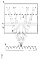
- Fig. 7 illustrates a microlens array 37 and a conical optical-element array 40 disposed on the entrant-light side of the liquid-crystal panel 14.
- the conical optical-element array 40, the microlens array 37 and the liquid-crystal panel 14 are arranged in the order mentioned along the traveling direction of the incident light.
- the conical optical-element array 40 and the microlens array 37 are provided between the condenser lens 13 and the liquid-crystal panel 14. The position of the polarizer 15 will be described later.
- the conical optical-element array 40 is constituted by a transparent body and comprises a substrate 42 and a multiplicity of conical optical elements 41 fixedly arrayed in two dimensions on the substrate 42.
- the conical optical elements 41, microlenses 38 and pixels E (apertures A) are in one-to-one correspondence, and mutually corresponding ones of these elements, lenses and pixels are arrayed on a straight line lying parallel to the optic axis of the optical system shown in Fig. 1.
- each conical element 41 has a shape obtained by sectioning the apex of a quadrangular cone (pyramid) by a plane parallel to the base of the cone.
- the face which is the base of the quadrangular cone is an aperture 41b on the side at which the incident light enters
- the face formed by cutting off the apex is an aperture 41a on the side from which light exits.
- the area of the aperture 41a on the emergent-light side is smaller than the area of the aperture 41b on the light-incident side.
- Light rays L1, L2 incident upon the conical optical element 41 from the aperture 41b on the light-incident side are totally reflected at the side surfaces of the conical optical element 41 and emerge from the emergent-side aperture 41a while diverging.
- the shape of the conical optical element 41 is so designed that the incident light rays L1, L2 will emerge upon being total reflected only one time at the side surfaces of the element.
- the aperture 41a on the light-emergent side of the conical optical element serves as a virtual light source.
- the light emerges from the aperture 41a just as if the aperture 41a were a light source.
- the size of the aperture 41a on the light-emergent side of the conical optical element 41 should be the same as that of the aperture A inside the liquid-crystal panel 14, through this depends also upon the image-forming magnification of the optical system constituted by the microlens 38. The reason is that if the image-forming magnification of the optical system is 1, a spot having a size the same as that of the light source can be formed.
- the conical optical-element array 40 described above can be fabricated by EB (electron-beam) lithography, a light exposure method or grinding method. Mass production is possible using a molding method that employs a mold (an injection molding method or a molding method using a resin that is hardened by infrared radiation).
- the shape of the conical optical element 41 is not limited to a quadrangular cone. Other shapes that can be adopted are a circular cone, a hexagonal cone and the like.
- Fig. 8b illustrates another example of a conical optical element.
- a conical optical element 43 is hollow and conical in shape and includes an aperture 43b on the light-incident side and an aperture 43a on the light-emergent side, with the area of the latter aperture being smaller than that of the former aperture.
- a reflecting film (e.g., a reflecting film made of metal) 44 is formed on the inner peripheral surface of the conical optical element 43.
- Light rays L1, L2 which impinge upon the interior of the conical optical element 43 from the aperture 43b on the light-incident side emerge from the aperture 43a on the light-emergent side upon being mirrored by the reflecting film 44, preferably only one time.
- microlenses 38 constructing the microlens array 37 are a double-convex lens, a Fresnel lens, a meniscus lens, a cylindrical lens and the like. The details will be set forth later.
- the microlens array 37 also can be fabricated by the methods mentioned above.
- Fig. 9 shows the positional relationship among the conical optical-element array 40, the microlens array 37 and the liquid-crystal panel 14, as well as the manner in which light is emitted from the conical optical-element array 40.
- Figs. 10 and 11 illustrated below only the conductive wiring pattern 24 is shown on the liquid-crystal panel 14.
- Fig. 10 illustrates the manner in which the light which has emerged from one conical optical element 41 of the conical optical-element array 40 has its image formed on the liquid-crystal panel 14 through the microlens array 37.
- the polarizer 15 is disposed on the light-incident side of the conical optical-element array 40.
- d1 represent the distance between the conical optical-element array 40 and the microlens array 37
- n1 the refractive index of the material (generally air) between the two arrays
- d2 the thickness of the microlens array 37 (the substrate thereof)
- n2 the refractive index of the microlens array
- d2 the thickness of the glass substrate 21 of the liquid-crystal panel 14 on the light-incident side
- n3 the refractive index of this glass substrate.
- the light which has emerged from the conical optical-element array 41 will have its image formed exactly on the apertures A within the liquid-crystal panel 14 through respective ones of several microlenses 38 of the microlens array 37.
- the size of the spot formed on the aperture A becomes approximately equal to the size of the aperture 41a on the light-emergent side of the conical optical-element array 41 (the size of the virtual light source).
- the size of the spot formed on the aperture A becomes smaller than the size of the aperture 41a on the light-emergent side when C/D is set to be equal to 2, 3, etc.
- the light which has exited from the conical optical element 41 is condensed at least by the microlens 38 corresponding thereto and the image of the light source is focused within the aperture A corresponding to this optical element. Since it is considered that the light intensity of the image of this light source is the greatest and that the light intensities of the images produced by the peripheral microlenses 38 are smaller, loss of light is not that great and the brightness of the image can be assured to a certain extent.
- the conical optical-element array 40 or microlens array 37 is fabricated using a resin material (e.g., polycarbonate or the like), the arrays 40, 37 will possess a birefringence characteristic.
- a resin material e.g., polycarbonate or the like
- the polarizer 15 is disposed on the light-incident side of the arrays 40, 37, an unfortunate consequence is that the light that has been converted into linearly polarized light by the polarizer 15 is converted into elliptically polarized light owing to the birefringence characteristic of the arrays when the light passes through them. When this occurs, some of the light unfortunately passes through the liquid-crystal panel 14 and the polarizer 16 even in a state in which no voltage is applied to the liquid-crystal panel 14.
- FIG. 11 A modification depicted in Fig. 11 illustrates an arrangement in which the above-mentioned problem is solved.
- the polarizer 15 is placed between the microlens array 37 and the liquid-crystal panel 14.
- the incident light which is natural light (randomly polarized light)
- the conical optical-element array 40 or microlens array 37 possesses a birefringence characteristic, the birefringence characteristic has no effect. Accordingly, a clear image in which the difference in brightness between dark and bright portions is large is obtained.
- d4/n4 should be added to the denominator on the left side of Eq. 1, in which d4 represents the thickness of the polarizer 15 and n4 the refractive index thereof.
- the need for the polarizer 15 can be eliminated. It is permissible to affix a polarizing film to the glass substrate 21.
- the substrate of the microlens array 37 can be made a polarizing plate.
- a number of the microlenses 38 can be formed on a polarizing film.
- Fig. 12 illustrates another embodiment of the invention.
- a microlens array 50 is provided on the light-incident side of the microlens array 37 instead of the conical optical-element array as the device for forming the virtual light sources.
- the microlens array 50 may have a construction the same as that of the microlens array 37.
- the microlens array 50 comprises a substrate 52 and a number of microlenses 51 arrayed two-dimensionally on the substrate 52.
- the microlenses 51 of the microlens array 50 and the microlenses 38 of the microlens array 37 are in one-to-one correspondence.
- Mutually corresponding ones of the microlenses 51, 38 and apertures A of the liquid-crystal panel 14 lie on a straight line that is parallel to the optic axis.
- Fig. 13 shows the positional relationship among the microlens array 50, the microlens array 37 and the liquid-crystal panel 14, as well as the manner in which a virtual light source a2b2 is formed by a microlens 51 of the microlens array 50.
- the polarizer 15 is omitted, but it goes without saying that the polarizer 15 can be disposed in the manner shown in Fig. 10 or Fig. 11.
- only the conductive wiring pattern 24 is shown in the liquid-crystal panel.
- the light source a2b2 has its image formed in front of the microlens 51 owing to impingement of light rays L1, L2 on the microlens 51 of the microlens array 50.
- the light source a2b2 serves as a virtual light source.
- the size of the light source a2b2 preferably is the same as that of the aperture A, as mentioned earlier.
- Virtual light sources of the kind a2b2 are formed in front of all of the microlenses 51.
- Fig. 14 illustrates the manner in which the virtual light source a2b2 has its image formed at the position of the aperture A of the liquid-crystal panel 14 by the microlens 38 of microlens array 37. Since a large amount of light emerges from the liquid-crystal panel 14 through the aperture A, in exactly the same manner as described earlier with reference to Figs. 10 and 11, a bright image can be obtained.
- Figs. 15a and 15b illustrate an example of the unified structure of the liquid-crystal panel 14 and microlens arrays 37, 50.
- the microlenses 38 are secured directly to the glass substrate (or polarizer) on the light-incident side of the liquid-crystal panel 14.
- the microlens array 50 is attached to the liquid-crystal panel 14 via a spacer 55.
- the substrate 39 of the microlens array 37 is secured to the liquid-crystal panel 14, and the microlens array 50 is secured to the liquid-crystal panel 14 via the spacer 55.
- Fig. 16 illustrates other examples of the microlens array 37 or 50.
- Figs. 16a and 16b illustrate a microlens array in which the microlenses are realized by double-convex lenses.
- Figs. 16c and 16d illustrate examples of cylindrical lenses.
- the conical optical-element array also may be replaced by an array of optical elements having an inclined surface in one direction only. In such case, linear virtual light sources would be formed.
Applications Claiming Priority (2)
| Application Number | Priority Date | Filing Date | Title |
|---|---|---|---|
| JP3169130A JP2959202B2 (ja) | 1991-06-14 | 1991-06-14 | 液晶パネルを用いた画像表示装置および液晶tvプロジェクタ |
| JP169130/91 | 1991-06-14 |
Publications (2)
| Publication Number | Publication Date |
|---|---|
| EP0518362A1 true EP0518362A1 (fr) | 1992-12-16 |
| EP0518362B1 EP0518362B1 (fr) | 1996-09-04 |
Family
ID=15880839
Family Applications (1)
| Application Number | Title | Priority Date | Filing Date |
|---|---|---|---|
| EP92109929A Expired - Lifetime EP0518362B1 (fr) | 1991-06-14 | 1992-06-12 | Dispositif d'affichage d'image utilisant un télé-projecteur à crystaux liquides et réseau d'éléments optiques coniques utilisés dans un tel dispositif |
Country Status (4)
| Country | Link |
|---|---|
| EP (1) | EP0518362B1 (fr) |
| JP (1) | JP2959202B2 (fr) |
| AT (1) | ATE142353T1 (fr) |
| DE (1) | DE69213339T2 (fr) |
Cited By (11)
| Publication number | Priority date | Publication date | Assignee | Title |
|---|---|---|---|---|
| WO1995014256A1 (fr) * | 1993-11-15 | 1995-05-26 | Alliedsignal Inc. | Element optique constituant d'un reseau d'elements optiques dans un agencement d'affichage |
| WO1995014255A1 (fr) * | 1993-11-19 | 1995-05-26 | Alliedsignal Inc. | Systeme d'eclairage par l'arriere pour affichage electro-optique |
| GB2289345A (en) * | 1994-05-06 | 1995-11-15 | Secretary Trade Ind Brit | An array of microlenses each assosciated with two pinholes |
| WO1996007115A1 (fr) * | 1994-08-26 | 1996-03-07 | Alliedsignal Inc. | Polariseur ameliore |
| WO1996021884A1 (fr) * | 1995-01-12 | 1996-07-18 | Alliedsignal Inc. | Ecran de visualisation a reseau de guides d'ondes coniques |
| US5689315A (en) * | 1992-07-15 | 1997-11-18 | Matsushita Electric Industrial Co., Ltd. | Light valve apparatus which is employed in a projection display system and in a view-finder system |
| US5748374A (en) * | 1995-12-01 | 1998-05-05 | U.S. Philips Corporation | Picture display device |
| EP0864897A2 (fr) * | 1997-02-27 | 1998-09-16 | Canon Kabushiki Kaisha | Dispositif de source de lumière, système d'éclairage et projecteur d'images |
| WO2002095489A1 (fr) * | 2001-05-23 | 2002-11-28 | Koninklijke Philips Electronics N.V. | Ecran cinematographique a cristaux liquides pourvu d'un collimateur |
| WO2002099772A2 (fr) * | 2001-06-01 | 2002-12-12 | Opto - System Gmbh | Procede permettant de modifier le comportement de rayonnement dans un element transparent plat de guidage de la lumiere et dispositifs equipes d'elements de ce type |
| US6545653B1 (en) | 1994-07-14 | 2003-04-08 | Matsushita Electric Industrial Co., Ltd. | Method and device for displaying image signals and viewfinder |
Families Citing this family (3)
| Publication number | Priority date | Publication date | Assignee | Title |
|---|---|---|---|---|
| JPH08114770A (ja) * | 1994-08-26 | 1996-05-07 | Omron Corp | 光学的ローパスフィルタおよびそれを利用したドットマトリクス表示装置 |
| EP0698804A3 (fr) | 1994-08-26 | 1998-09-02 | Omron Corporation | Dispositifs à cristaux liquides utilisant un filtre optique passe-bas et un polariseur |
| JP4089371B2 (ja) * | 2002-09-24 | 2008-05-28 | セイコーエプソン株式会社 | 透過型スクリーン及びリア型プロジェクタ |
Citations (2)
| Publication number | Priority date | Publication date | Assignee | Title |
|---|---|---|---|---|
| EP0267686A1 (fr) * | 1986-10-23 | 1988-05-18 | Litton Systems Canada Limited | Affichage à cristal liquide en couleur |
| EP0357070A2 (fr) * | 1988-09-01 | 1990-03-07 | Hughes Aircraft Company | Ecran de diffusion courbé à fibre optique avec contraste élevé |
-
1991
- 1991-06-14 JP JP3169130A patent/JP2959202B2/ja not_active Expired - Fee Related
-
1992
- 1992-06-12 EP EP92109929A patent/EP0518362B1/fr not_active Expired - Lifetime
- 1992-06-12 AT AT92109929T patent/ATE142353T1/de not_active IP Right Cessation
- 1992-06-12 DE DE69213339T patent/DE69213339T2/de not_active Expired - Fee Related
Patent Citations (2)
| Publication number | Priority date | Publication date | Assignee | Title |
|---|---|---|---|---|
| EP0267686A1 (fr) * | 1986-10-23 | 1988-05-18 | Litton Systems Canada Limited | Affichage à cristal liquide en couleur |
| EP0357070A2 (fr) * | 1988-09-01 | 1990-03-07 | Hughes Aircraft Company | Ecran de diffusion courbé à fibre optique avec contraste élevé |
Non-Patent Citations (2)
| Title |
|---|
| ELECTRONICS. DE 1984 A 1985 : ELECTRONICS WEEK vol. 58, no. 16, 22 April 1985, NEW YORK US pages 56 - 60 H.BIERMAN AND D.M.WEBER 'new display formats give users better show for fewer bucks' * |
| PATENT ABSTRACTS OF JAPAN vol. 14, no. 289 (P-1065)21 June 1990 & JP-A-20 89 025 ( NIPPON SHEET GLASS CO LTD ) * |
Cited By (17)
| Publication number | Priority date | Publication date | Assignee | Title |
|---|---|---|---|---|
| US5689315A (en) * | 1992-07-15 | 1997-11-18 | Matsushita Electric Industrial Co., Ltd. | Light valve apparatus which is employed in a projection display system and in a view-finder system |
| WO1995014256A1 (fr) * | 1993-11-15 | 1995-05-26 | Alliedsignal Inc. | Element optique constituant d'un reseau d'elements optiques dans un agencement d'affichage |
| KR100359532B1 (ko) * | 1993-11-15 | 2003-06-09 | 알라이드시그날 인코포레이티드 | 디스플레이배열에사용되는광학요소 |
| WO1995014255A1 (fr) * | 1993-11-19 | 1995-05-26 | Alliedsignal Inc. | Systeme d'eclairage par l'arriere pour affichage electro-optique |
| US5598281A (en) * | 1993-11-19 | 1997-01-28 | Alliedsignal Inc. | Backlight assembly for improved illumination employing tapered optical elements |
| GB2289345A (en) * | 1994-05-06 | 1995-11-15 | Secretary Trade Ind Brit | An array of microlenses each assosciated with two pinholes |
| GB2289345B (en) * | 1994-05-06 | 1998-02-18 | Secretary Trade Ind Brit | Array of microlenses each associated with two pinholes |
| US6545653B1 (en) | 1994-07-14 | 2003-04-08 | Matsushita Electric Industrial Co., Ltd. | Method and device for displaying image signals and viewfinder |
| WO1996007115A1 (fr) * | 1994-08-26 | 1996-03-07 | Alliedsignal Inc. | Polariseur ameliore |
| WO1996021884A1 (fr) * | 1995-01-12 | 1996-07-18 | Alliedsignal Inc. | Ecran de visualisation a reseau de guides d'ondes coniques |
| US5748374A (en) * | 1995-12-01 | 1998-05-05 | U.S. Philips Corporation | Picture display device |
| US6231193B1 (en) | 1997-02-27 | 2001-05-15 | Canon Kabushiki Kaisha | Light source device, illuminating system and image projecting apparatus |
| EP0864897A3 (fr) * | 1997-02-27 | 1998-10-28 | Canon Kabushiki Kaisha | Dispositif de source de lumière, système d'éclairage et projecteur d'images |
| EP0864897A2 (fr) * | 1997-02-27 | 1998-09-16 | Canon Kabushiki Kaisha | Dispositif de source de lumière, système d'éclairage et projecteur d'images |
| WO2002095489A1 (fr) * | 2001-05-23 | 2002-11-28 | Koninklijke Philips Electronics N.V. | Ecran cinematographique a cristaux liquides pourvu d'un collimateur |
| WO2002099772A2 (fr) * | 2001-06-01 | 2002-12-12 | Opto - System Gmbh | Procede permettant de modifier le comportement de rayonnement dans un element transparent plat de guidage de la lumiere et dispositifs equipes d'elements de ce type |
| WO2002099772A3 (fr) * | 2001-06-01 | 2003-04-03 | Opto System Gmbh | Procede permettant de modifier le comportement de rayonnement dans un element transparent plat de guidage de la lumiere et dispositifs equipes d'elements de ce type |
Also Published As
| Publication number | Publication date |
|---|---|
| ATE142353T1 (de) | 1996-09-15 |
| JPH04366917A (ja) | 1992-12-18 |
| DE69213339D1 (de) | 1996-10-10 |
| JP2959202B2 (ja) | 1999-10-06 |
| DE69213339T2 (de) | 1997-04-24 |
| EP0518362B1 (fr) | 1996-09-04 |
Similar Documents
| Publication | Publication Date | Title |
|---|---|---|
| EP0366462B1 (fr) | Appareil d'affichage d'image par projection | |
| KR0181725B1 (ko) | 통합 광을 제한하는 활성 매트릭스 액정 감색 디스플레이 | |
| US5150138A (en) | Projection type image display apparatus | |
| US5098184A (en) | Optical illumination system and projection apparatus comprising such a system | |
| US6147732A (en) | Dot matrix-type display device with optical low-pass filter fixed to a member via an adhesive bonding | |
| KR100381827B1 (ko) | 컬러액정투사디스플레이시스템 | |
| KR950006359B1 (ko) | 컬러액정 표시장치 | |
| EP0518362B1 (fr) | Dispositif d'affichage d'image utilisant un télé-projecteur à crystaux liquides et réseau d'éléments optiques coniques utilisés dans un tel dispositif | |
| KR100262044B1 (ko) | 화상표시장치 | |
| EP0644450A1 (fr) | Appareil d'affichage d'image | |
| US5455694A (en) | Liquid crystal display with pixel shape same as image of light source through microlens | |
| US5359440A (en) | Image display apparatus with microlens plate having mutually fused together lenses resulting in hexagonal shaped microlenses | |
| JPH06102509A (ja) | 光カップリング・レンズアレイ付きフルカラー表示装置 | |
| KR19990008170A (ko) | 광변조 디바이스, 표시 장치 및 전자 기기 | |
| JPH0351882A (ja) | 投影形画像表示装置 | |
| WO1996002113A1 (fr) | Systemes d'affichage par projection a cristaux liquides en couleur | |
| KR100231979B1 (ko) | 표시장치, 액정표시패널 및 이를 사용한 투사형 표시장치 | |
| US5430562A (en) | Liquid crystal light valve including between light and light valve microlenses and two reflecting layers with a matrix of openings | |
| KR940006985B1 (ko) | 영상표시장치 | |
| US5990993A (en) | Display device having a backlighting system supplying collimated light | |
| JP3331238B2 (ja) | 直視型表示装置 | |
| JPH04251221A (ja) | 液晶表示装置及びこれを用いる投写型表示装置 | |
| JP3146607B2 (ja) | 液晶tvプロジェクタ | |
| JPH03278026A (ja) | 反射型液晶表示素子 | |
| JPH02302726A (ja) | 液晶表示素子 |
Legal Events
| Date | Code | Title | Description |
|---|---|---|---|
| PUAI | Public reference made under article 153(3) epc to a published international application that has entered the european phase |
Free format text: ORIGINAL CODE: 0009012 |
|
| 17P | Request for examination filed |
Effective date: 19920709 |
|
| AK | Designated contracting states |
Kind code of ref document: A1 Designated state(s): AT BE CH DE DK ES FR GB GR IT LI LU MC NL PT SE |
|
| 17Q | First examination report despatched |
Effective date: 19941118 |
|
| GRAH | Despatch of communication of intention to grant a patent |
Free format text: ORIGINAL CODE: EPIDOS IGRA |
|
| GRAH | Despatch of communication of intention to grant a patent |
Free format text: ORIGINAL CODE: EPIDOS IGRA |
|
| GRAA | (expected) grant |
Free format text: ORIGINAL CODE: 0009210 |
|
| AK | Designated contracting states |
Kind code of ref document: B1 Designated state(s): AT BE CH DE DK ES FR GB GR IT LI LU MC NL PT SE |
|
| PG25 | Lapsed in a contracting state [announced via postgrant information from national office to epo] |
Ref country code: DK Effective date: 19960904 Ref country code: CH Effective date: 19960904 Ref country code: ES Free format text: THE PATENT HAS BEEN ANNULLED BY A DECISION OF A NATIONAL AUTHORITY Effective date: 19960904 Ref country code: LI Effective date: 19960904 Ref country code: AT Effective date: 19960904 Ref country code: BE Effective date: 19960904 Ref country code: GR Free format text: LAPSE BECAUSE OF FAILURE TO SUBMIT A TRANSLATION OF THE DESCRIPTION OR TO PAY THE FEE WITHIN THE PRESCRIBED TIME-LIMIT Effective date: 19960904 |
|
| REF | Corresponds to: |
Ref document number: 142353 Country of ref document: AT Date of ref document: 19960915 Kind code of ref document: T |
|
| REF | Corresponds to: |
Ref document number: 69213339 Country of ref document: DE Date of ref document: 19961010 |
|
| ITF | It: translation for a ep patent filed |
Owner name: STUDIO TORTA SOCIETA' SEMPLICE |
|
| ET | Fr: translation filed | ||
| PG25 | Lapsed in a contracting state [announced via postgrant information from national office to epo] |
Ref country code: PT Effective date: 19961204 Ref country code: SE Effective date: 19961204 |
|
| REG | Reference to a national code |
Ref country code: CH Ref legal event code: PL |
|
| PG25 | Lapsed in a contracting state [announced via postgrant information from national office to epo] |
Ref country code: LU Free format text: LAPSE BECAUSE OF NON-PAYMENT OF DUE FEES Effective date: 19970630 |
|
| PLBE | No opposition filed within time limit |
Free format text: ORIGINAL CODE: 0009261 |
|
| STAA | Information on the status of an ep patent application or granted ep patent |
Free format text: STATUS: NO OPPOSITION FILED WITHIN TIME LIMIT |
|
| 26N | No opposition filed | ||
| PG25 | Lapsed in a contracting state [announced via postgrant information from national office to epo] |
Ref country code: MC Effective date: 19971231 |
|
| PGFP | Annual fee paid to national office [announced via postgrant information from national office to epo] |
Ref country code: NL Payment date: 19980619 Year of fee payment: 7 |
|
| PG25 | Lapsed in a contracting state [announced via postgrant information from national office to epo] |
Ref country code: NL Free format text: LAPSE BECAUSE OF NON-PAYMENT OF DUE FEES Effective date: 20000101 |
|
| NLV4 | Nl: lapsed or anulled due to non-payment of the annual fee |
Effective date: 20000101 |
|
| REG | Reference to a national code |
Ref country code: GB Ref legal event code: IF02 |
|
| PG25 | Lapsed in a contracting state [announced via postgrant information from national office to epo] |
Ref country code: IT Free format text: LAPSE BECAUSE OF NON-PAYMENT OF DUE FEES;WARNING: LAPSES OF ITALIAN PATENTS WITH EFFECTIVE DATE BEFORE 2007 MAY HAVE OCCURRED AT ANY TIME BEFORE 2007. THE CORRECT EFFECTIVE DATE MAY BE DIFFERENT FROM THE ONE RECORDED. Effective date: 20050612 |
|
| PGFP | Annual fee paid to national office [announced via postgrant information from national office to epo] |
Ref country code: DE Payment date: 20080630 Year of fee payment: 17 |
|
| PGFP | Annual fee paid to national office [announced via postgrant information from national office to epo] |
Ref country code: FR Payment date: 20080613 Year of fee payment: 17 |
|
| PGFP | Annual fee paid to national office [announced via postgrant information from national office to epo] |
Ref country code: GB Payment date: 20080612 Year of fee payment: 17 |
|
| GBPC | Gb: european patent ceased through non-payment of renewal fee |
Effective date: 20090612 |
|
| REG | Reference to a national code |
Ref country code: FR Ref legal event code: ST Effective date: 20100226 |
|
| PG25 | Lapsed in a contracting state [announced via postgrant information from national office to epo] |
Ref country code: FR Free format text: LAPSE BECAUSE OF NON-PAYMENT OF DUE FEES Effective date: 20090630 |
|
| PGFP | Annual fee paid to national office [announced via postgrant information from national office to epo] |
Ref country code: IT Payment date: 20080625 Year of fee payment: 17 |
|
| PGRI | Patent reinstated in contracting state [announced from national office to epo] |
Ref country code: IT Effective date: 20091201 |
|
| PG25 | Lapsed in a contracting state [announced via postgrant information from national office to epo] |
Ref country code: GB Free format text: LAPSE BECAUSE OF NON-PAYMENT OF DUE FEES Effective date: 20090612 |
|
| PG25 | Lapsed in a contracting state [announced via postgrant information from national office to epo] |
Ref country code: DE Free format text: LAPSE BECAUSE OF NON-PAYMENT OF DUE FEES Effective date: 20100101 |
|
| PGRI | Patent reinstated in contracting state [announced from national office to epo] |
Ref country code: IT Effective date: 20091201 |
|
| REG | Reference to a national code |
Ref country code: DE Ref legal event code: R082 Ref document number: 69213339 Country of ref document: DE Representative=s name: KILIAN KILIAN & PARTNER, DE |