EP0517727B1 - Process for producing an insulated monocrystalline silicon island - Google Patents
Process for producing an insulated monocrystalline silicon island Download PDFInfo
- Publication number
- EP0517727B1 EP0517727B1 EP91904136A EP91904136A EP0517727B1 EP 0517727 B1 EP0517727 B1 EP 0517727B1 EP 91904136 A EP91904136 A EP 91904136A EP 91904136 A EP91904136 A EP 91904136A EP 0517727 B1 EP0517727 B1 EP 0517727B1
- Authority
- EP
- European Patent Office
- Prior art keywords
- layer
- silicon
- process according
- doping
- mask
- Prior art date
- Legal status (The legal status is an assumption and is not a legal conclusion. Google has not performed a legal analysis and makes no representation as to the accuracy of the status listed.)
- Expired - Lifetime
Links
Images


Classifications
-
- H—ELECTRICITY
- H01—ELECTRIC ELEMENTS
- H01L—SEMICONDUCTOR DEVICES NOT COVERED BY CLASS H10
- H01L21/00—Processes or apparatus adapted for the manufacture or treatment of semiconductor or solid state devices or of parts thereof
- H01L21/02—Manufacture or treatment of semiconductor devices or of parts thereof
- H01L21/04—Manufacture or treatment of semiconductor devices or of parts thereof the devices having at least one potential-jump barrier or surface barrier, e.g. PN junction, depletion layer or carrier concentration layer
- H01L21/18—Manufacture or treatment of semiconductor devices or of parts thereof the devices having at least one potential-jump barrier or surface barrier, e.g. PN junction, depletion layer or carrier concentration layer the devices having semiconductor bodies comprising elements of Group IV of the Periodic System or AIIIBV compounds with or without impurities, e.g. doping materials
- H01L21/26—Bombardment with radiation
- H01L21/263—Bombardment with radiation with high-energy radiation
- H01L21/265—Bombardment with radiation with high-energy radiation producing ion implantation
- H01L21/26506—Bombardment with radiation with high-energy radiation producing ion implantation in group IV semiconductors
- H01L21/26533—Bombardment with radiation with high-energy radiation producing ion implantation in group IV semiconductors of electrically inactive species in silicon to make buried insulating layers
-
- H—ELECTRICITY
- H01—ELECTRIC ELEMENTS
- H01L—SEMICONDUCTOR DEVICES NOT COVERED BY CLASS H10
- H01L21/00—Processes or apparatus adapted for the manufacture or treatment of semiconductor or solid state devices or of parts thereof
- H01L21/70—Manufacture or treatment of devices consisting of a plurality of solid state components formed in or on a common substrate or of parts thereof; Manufacture of integrated circuit devices or of parts thereof
- H01L21/71—Manufacture of specific parts of devices defined in group H01L21/70
- H01L21/76—Making of isolation regions between components
- H01L21/762—Dielectric regions, e.g. EPIC dielectric isolation, LOCOS; Trench refilling techniques, SOI technology, use of channel stoppers
- H01L21/7624—Dielectric regions, e.g. EPIC dielectric isolation, LOCOS; Trench refilling techniques, SOI technology, use of channel stoppers using semiconductor on insulator [SOI] technology
- H01L21/76264—SOI together with lateral isolation, e.g. using local oxidation of silicon, or dielectric or polycristalline material refilled trench or air gap isolation regions, e.g. completely isolated semiconductor islands
- H01L21/76267—Vertical isolation by silicon implanted buried insulating layers, e.g. oxide layers, i.e. SIMOX techniques
-
- H—ELECTRICITY
- H01—ELECTRIC ELEMENTS
- H01L—SEMICONDUCTOR DEVICES NOT COVERED BY CLASS H10
- H01L21/00—Processes or apparatus adapted for the manufacture or treatment of semiconductor or solid state devices or of parts thereof
- H01L21/70—Manufacture or treatment of devices consisting of a plurality of solid state components formed in or on a common substrate or of parts thereof; Manufacture of integrated circuit devices or of parts thereof
- H01L21/71—Manufacture of specific parts of devices defined in group H01L21/70
- H01L21/76—Making of isolation regions between components
- H01L21/762—Dielectric regions, e.g. EPIC dielectric isolation, LOCOS; Trench refilling techniques, SOI technology, use of channel stoppers
- H01L21/7624—Dielectric regions, e.g. EPIC dielectric isolation, LOCOS; Trench refilling techniques, SOI technology, use of channel stoppers using semiconductor on insulator [SOI] technology
- H01L21/76264—SOI together with lateral isolation, e.g. using local oxidation of silicon, or dielectric or polycristalline material refilled trench or air gap isolation regions, e.g. completely isolated semiconductor islands
- H01L21/76281—Lateral isolation by selective oxidation of silicon
-
- H—ELECTRICITY
- H01—ELECTRIC ELEMENTS
- H01L—SEMICONDUCTOR DEVICES NOT COVERED BY CLASS H10
- H01L21/00—Processes or apparatus adapted for the manufacture or treatment of semiconductor or solid state devices or of parts thereof
- H01L21/70—Manufacture or treatment of devices consisting of a plurality of solid state components formed in or on a common substrate or of parts thereof; Manufacture of integrated circuit devices or of parts thereof
- H01L21/71—Manufacture of specific parts of devices defined in group H01L21/70
- H01L21/76—Making of isolation regions between components
- H01L21/762—Dielectric regions, e.g. EPIC dielectric isolation, LOCOS; Trench refilling techniques, SOI technology, use of channel stoppers
- H01L21/7624—Dielectric regions, e.g. EPIC dielectric isolation, LOCOS; Trench refilling techniques, SOI technology, use of channel stoppers using semiconductor on insulator [SOI] technology
- H01L21/76264—SOI together with lateral isolation, e.g. using local oxidation of silicon, or dielectric or polycristalline material refilled trench or air gap isolation regions, e.g. completely isolated semiconductor islands
- H01L21/76283—Lateral isolation by refilling of trenches with dielectric material
-
- H—ELECTRICITY
- H01—ELECTRIC ELEMENTS
- H01L—SEMICONDUCTOR DEVICES NOT COVERED BY CLASS H10
- H01L21/00—Processes or apparatus adapted for the manufacture or treatment of semiconductor or solid state devices or of parts thereof
- H01L21/70—Manufacture or treatment of devices consisting of a plurality of solid state components formed in or on a common substrate or of parts thereof; Manufacture of integrated circuit devices or of parts thereof
- H01L21/71—Manufacture of specific parts of devices defined in group H01L21/70
- H01L21/76—Making of isolation regions between components
- H01L21/762—Dielectric regions, e.g. EPIC dielectric isolation, LOCOS; Trench refilling techniques, SOI technology, use of channel stoppers
- H01L21/7624—Dielectric regions, e.g. EPIC dielectric isolation, LOCOS; Trench refilling techniques, SOI technology, use of channel stoppers using semiconductor on insulator [SOI] technology
- H01L21/76264—SOI together with lateral isolation, e.g. using local oxidation of silicon, or dielectric or polycristalline material refilled trench or air gap isolation regions, e.g. completely isolated semiconductor islands
- H01L21/76286—Lateral isolation by refilling of trenches with polycristalline material
-
- H—ELECTRICITY
- H01—ELECTRIC ELEMENTS
- H01L—SEMICONDUCTOR DEVICES NOT COVERED BY CLASS H10
- H01L21/00—Processes or apparatus adapted for the manufacture or treatment of semiconductor or solid state devices or of parts thereof
- H01L21/70—Manufacture or treatment of devices consisting of a plurality of solid state components formed in or on a common substrate or of parts thereof; Manufacture of integrated circuit devices or of parts thereof
- H01L21/71—Manufacture of specific parts of devices defined in group H01L21/70
- H01L21/76—Making of isolation regions between components
- H01L21/762—Dielectric regions, e.g. EPIC dielectric isolation, LOCOS; Trench refilling techniques, SOI technology, use of channel stoppers
- H01L21/7624—Dielectric regions, e.g. EPIC dielectric isolation, LOCOS; Trench refilling techniques, SOI technology, use of channel stoppers using semiconductor on insulator [SOI] technology
- H01L21/76264—SOI together with lateral isolation, e.g. using local oxidation of silicon, or dielectric or polycristalline material refilled trench or air gap isolation regions, e.g. completely isolated semiconductor islands
- H01L21/76289—Lateral isolation by air gap
Definitions
- the present invention relates to a method for producing an isolated, single-crystal silicon island.
- the subject of the invention is thus a procedural part of the manufacturing process of an integrated microelectronic circuit.
- the oxygen implantation is carried out within the epitaxially grown layers, so that a subsequent high-temperature annealing process is required, in which the doping of the different layers runs into one another, so that one can choose the desired ones Doping sequences are severely restricted.
- DE-A1-24 51 861 already discloses a method for producing an insulated, single-crystalline silicon island within a silicon substrate, in which the silicon island is separated from the substrate by a dielectric insulation layer.
- essentially V-shaped trenches are first produced using anisotropic etching. If desired, an n ein layer can now be diffused in.
- An insulating oxide layer is then grown.
- a polysilicon layer is now deposited with a layer thickness of approximately 250 micrometers, which forms the subsequent substrate layer.
- the single-crystalline silicon layer is then mechanically ground down until the islands are isolated. Lateral low-voltage components or power components can be integrated into these islands.
- the US-A-3976511 shows a method for producing an isolated, single-crystalline silicon layer, in which a buried, electrically insulating SiO2 layer is first generated starting from a substrate with a doping of approximately 2 x 10¹⁶ atoms / cm3 by oxygen implantation. After the resulting layer structure has been thermally healed, a monocrystalline epitaxial layer is grown. After this process step, the silicon wafer is turned over, whereupon the former substrate layer is removed by etching. The buried insulator serves as an etch stop. The result is isolated, single-crystalline silicon islands. This method is not adapted to the standard manufacturing process for integrated electronic circuits.
- the present invention has for its object to provide a method for producing an isolated, single-crystalline silicon island, which can be easily inserted into the manufacturing process for integrated electronic circuits on the one hand and which results in improved electrical insulation of the silicon island produced on the other hand.
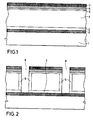
- the process sequence for producing the isolated, single-crystal silicon island begins with the choice of a highly doped, single-crystal substrate 1.
- a highly doped substrate In the case of an n+ substrate 1, this can be done with arsenic or antimony be endowed.
- a p+-doped Substrate can include the dopants boron.
- a highly doped substrate is not desired, a low-doped substrate can also be used, the layer close to the surface of which is heavily doped by ion implantation and is subsequently cured. In this case, the doping of the layer close to the surface must be carried out before the oxygen implantation explained below, since a silicon layer lying on a buried insulator is amorphized during the dopant implantation and no longer heals in a single crystal.
- the layer system 1, 2, 3 produced in this way is now thermally cured, so that the n+-silicon layer 3 becomes a high-quality, single-crystal layer with low resistance.
- a silicon epitaxial layer 4 with low n or p doping is then deposited with a preferred thickness of 1 to 10 micrometers.
- a pad oxide layer 5 with a thickness of approximately 8 to 25 nm is deposited on this 4 or produced by thermal growth.
- a nitride layer 6 with a thickness of 100 to 200 nm is deposited on the pad oxide layer 5 and serves as a diffusion barrier in later diffusion steps.
- a final oxide layer 7 with a thickness of approximately 1 micron is deposited on the nitride layer 6.
- the width of the later trench trenches provided in the preferred embodiment is 1 to 1.5 micrometers.
- the trenches 8 are etched up to the buried SiO 2 layer serving as an etching stop mask, as is illustrated in FIG. 2.
- the nitride layer 6 serves as a diffusion barrier to protect the semiconductor wafer surface covered by it.
- the trench side walls 9 are now insulated by thermal oxidation to produce a thermal side wall oxide layer 10.
- thermal oxidation oxide deposition can of course also be used to produce a deposited sidewall oxide layer.
- the trenches 8 are now filled with polysilicon. It is also possible to fill the trenches 8 with TEOS oxide.
- the final oxide layer 7 is removed.
- the polysilicon 11 is locally oxidized in the region of the surface of the trenches 8 on the upper side of the semiconductor wafer (see reference number 12 in FIG. 3) in order to isolate the trenches 8.
- the nitride layer 6 serves as a mask.
- the nitride layer 6 is now removed. This completes the actual process for producing the isolated, single-crystalline silicon island.
- the desired components can now be introduced into the silicon islands. These components can be NMOS, PMOS or bipolar transistors, quasi-vertical power transistors, lateral high-voltage transistors or other elements.
- a lightly doped substrate with a highly doped near-surface layer which is produced by ion implantation and annealing, can be used.
- This doping implantation can be limited locally by first creating a doping implantation mask by photolithography before the high doping of the layer near the surface is carried out.
- a mask can be used in the oxygen implantation to produce the buried SiO2 layer, so that the silicon epitaxial layer is connected directly to the substrate 1 outside the region of the buried SiO2 layer 2, as is, inter alia, in the exemplary embodiment explained below according to FIG 4 is the case.
- the structure described with reference to FIGS. 1 to 3 is limited in its dielectric strength due to the breakdown voltage of the buried SiO2 layer 2. With a thickness of this layer of 0.35 micrometers, as chosen in the preferred embodiment, a breakdown voltage of approximately 250 V results. For reasons of the trench etching technique, the trench depth and thus the thickness of the epitaxially grown layer 4 should be less than 10 micrometers lie.
- the breakdown voltage of vertical components integrated outside the silicon islands is thus limited to less than 150 V. If if it is desired to give breakdown voltages of above 150 V to these vertical components integrated outside the silicon islands, the breakdown voltage can be increased in the exemplary embodiment of FIG. 4 to be explained, depending on the choice of the oxide breakdown voltage technique used, which is yet to be explained SiO2 layer 2 correspond or which are almost arbitrarily high, as is the case in the embodiment of FIG. 5.
- a single-crystalline silicon epitaxial layer 4a with a first layer thickness is first grown on the highly doped substrate 1. This process step is followed by the local high doping of this first silicon epitaxial layer 4a by means of ion implantation using a doping mask. After this doping, the layer system 1, 4a produced in this way is healed. Now the oxygen implantation into the doped silicon epitaxial layer 4a for producing the buried, insulated SiO2 layer 2 is carried out using the aforementioned doping mask. The structure produced is then thermally healed. A second silicon epitaxial layer 4b is then grown with a second layer thickness. The layer thickness of the second silicon epitaxial layer 4b is 1 to 10 micrometers.
- the thickness of the first-mentioned silicon epitaxial layer is below the total thickness required for the dielectric strength by the thickness of the second silicon epitaxial layer.
- the epitaxial layer thickness on the buried oxide 2 is therefore at a value suitable for carrying out the trench insulation of 1 to 10 micrometers, while the total thickness of the two epitaxial layers 4a, 4b is adapted outside the region of the SiO2 layer 2 to the desired breakdown voltage.
- the embodiment according to FIG. 4 thus has a dielectric strength of the silicon islands up to the breakdown voltage of the, while maintaining a trench depth of at most 10 micrometers buried oxide or the SiO2 layer of about 250 V.
- FIG. 5 can be considered.
- a deep implantation of dopants under the SiO2 layer 2 is carried out before the growth of the second epitaxial silicon layer 4b using a doping mask in order to produce the structure according to FIG. 5, so that below the insulating SiO2 layer 2 forms a layer 13 doped opposite to substrate 1.
- This layer 13, which is doped in opposition to the substrate 1, is guided to the semiconductor wafer surface by means of a contacting region 14.
- the contacting region 14 can either be produced by deep diffusion after the epitaxial growth of the second silicon layer 4b.
- doping of the trench side wall 9 can also be considered for producing a conductive connection between the opposite substrate 1 doped layer 13 and the wafer surface.
- the silicon islands have a dielectric strength of more than 1000 V. This high dielectric strength is achieved by applying a fixed potential to the layer 13, which leads to a polarity of the pn junction adjacent to the layer 13 in Blocking direction leads. Most of the voltage drops at the pn junction formed in the substrate.
- FIGS. 6 to 8 are formed according to the invention, which are explained below together with their production method.
- Thermal insulation of components is of interest, for example, when these components are, for example, transistors in gas sensors that are used in over 150 ° C are to be operated. If such components can be arranged in a thermally insulated manner, the remaining circuit area remains cool compared to the heated circuit area, so that a low heating power is sufficient.
- the starting structure used is one such as that shown in FIGS. 1 to 3 and explained at the outset with regard to its production method.
- the highly doped silicon epitaxial layer 3 or the doping of the side wall 9 can be omitted.
- the silicon region 1, 4 can also be a low-doped region. Both full-area and partial oxygen implantations are also possible.
- the following additional steps are carried out:
- the back of the semiconductor wafer is provided with a back mask, which can consist of silicon nitride or oxide.
- the mask on the back of the pane is opened locally by means of photolithographic measures.
- the etching mask produced in this way serves to mask the subsequent anisotropic etching of the silicon wafer from its rear side, the buried SiO 2 layer 2 serving as an etching stop in this etching process.
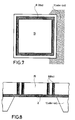
- a silicon membrane 15 is generated, the thickness of which corresponds to the sum of the thicknesses of the buried SiO2 layer, the n+-silicon layer 3, insofar as this is provided, and the silicon epitaxial layer 4.
- the thickness of the silicon membrane 15 produced is 2 to 10 micrometers. Their doping is determined by the epitaxy. The size of the membrane is determined from the mask opening on the back of the pane and the etching angle of the anisotropic etching solution, which is, for example, 54.7 ° in the case of a 100 silicon substrate.
- the semiconductor structure produced in this way has a thermally insulated silicon membrane 15, since the membrane layer 15 is insulated upwards and downwards by air, and the lateral insulation is formed by at least one trench 8 which surrounds the silicon island and lies on the etched-off surface itself .
- a heat transfer can now only take place via the air or the trench 8, which is at least partially filled with oxide, which has a high thermal resistance due to the low thermal conductivity of oxide.
- oxide which has a high thermal resistance due to the low thermal conductivity of oxide.
- it is either filled with oxide and polysilicon or completely filled with a CVD oxide, as can be the case, for example, with TEOS.
- the heat transfer can now only take place laterally via the trench.
- a trench filled with a deposited oxide or thermal oxide or polysilicon with an effective oxide thickness of 1 micron has a thermal insulation effect which corresponds to that of a silicon membrane with a width of 100 microns, since the thermal conductivity of oxide corresponds to only one 100th of that of silicon.
- FIG. 7 The top view of the resulting membrane structure is shown in FIG. 7.
- trenches 8 can be thermally connected in series, as can be seen in the embodiment of FIG. 8.
- two or more trenches are concentric with each other around the silicon island, with all trenches lying on the etched-off surface.
- the result is a very compact and therefore stable thermal insulation of a thin silicon membrane 15.
- This is single-crystalline due to the method according to the invention. It can therefore be integrated, for example, for the integration of a sensor element with heating and temperature measurement.
Abstract
Description
Die vorliegende Erfindung befaßt sich mit einem Verfahren zum Erzeugen einer isolierten, einkristallinen Siliziuminsel. Der Erfindungsgegenstand ist somit ein verfahrensmäßiger Bestandteil des Herstellungsprozesses einer integrierten mikroelektronischen Schaltung.The present invention relates to a method for producing an isolated, single-crystal silicon island. The subject of the invention is thus a procedural part of the manufacturing process of an integrated microelectronic circuit.
Aus der Fachzeitschrift Electronics, 26. November 1987, Seiten 127 bis 129 sowie aus der US-A-38 97 274 sind bereits Verfahren zum Erzeugen isolierter Siliziuminseln bekannt, bei denen eine vergrabene Siliziumdioxidschicht zur Isolation der Siliziuminsel durch Ionenimplantation erzeugt wird, woraufhin eine Trenchätzmaske zur Definition der Trenches zur lateralen Begrenzung der Siliziuminsel gebildet wird, mit deren Hilfe Trenches bis zu der vergrabenen Siliziumdioxidschicht geätzt werden, welche anschließend mit einem Dielektrikum aufgefüllt werden. Bei dem Verfahren nach der US-A-38 97 274 wird die Sauerstoffimplantation innerhalb der epitaxial aufgewachsenen Schichten durchgeführt, so daß ein anschließendes Hochtemperatur-Ausheilverfahren erforderlich wird, bei dem die Dotierungen der verschiedenen Schichten ineinander verlaufen, so daß man in der Wahl der gewünschten Dotierfolgen stark eingeschränkt ist. Alternativ ist es für den Fall von niedrigen gewünschten Beschleunigungsspannungen beschrieben, ausgehend von einem hochdotierten Substrat zunächst die Sauerstoffimplantation vorzunehmen, um sodann epitaxial aufgewachsene Schichten zu erzeugen. Wenn eine niedrige Dotierung des Substrates gefordert ist, ist diese Verfahrensalternative nicht anwendbar.Methods for producing isolated silicon islands are already known from the trade journal Electronics, November 26, 1987, pages 127 to 129 and from US-A-38 97 274, in which a buried silicon dioxide layer for isolating the silicon island is produced by ion implantation, whereupon a trench etching mask to define the trenches for the lateral delimitation of the silicon island, with the help of which trenches are etched up to the buried silicon dioxide layer, which are then filled with a dielectric. In the method according to US-A-38 97 274, the oxygen implantation is carried out within the epitaxially grown layers, so that a subsequent high-temperature annealing process is required, in which the doping of the different layers runs into one another, so that one can choose the desired ones Doping sequences are severely restricted. Alternatively, in the case of low desired acceleration voltages, it is described first to carry out the oxygen implantation starting from a heavily doped substrate, in order then to produce epitaxially grown layers. If a low doping of the substrate is required, this alternative method cannot be used.
Aus der EP-A-03 28 331 A2 ist es bekannt, bei dem Ätzen von Trenches eine Trenchätzmaske vorzusehen, die Trenches bis zu einer vergrabenen Oxidschicht zu ätzen, eine hohe Dotierung in die Trenchseitenwände einzubringen, um sodann die Trenches zu isolieren und aufzufüllen.From EP-A-03 28 331 A2 it is known to provide a trench etching mask when etching trenches, to etch the trenches up to a buried oxide layer, to introduce a high level of doping into the trench side walls, in order then to apply the trenches to isolate and replenish.
Aus der EP-A-03 25 161 A2 ist es bekannt, zum Auffüllen der Trenches Polysilizium zu verwenden.From EP-A-03 25 161 A2 it is known to use polysilicon to fill the trenches.
Aus der DE-A1-24 51 861 ist bereits ein Verfahren zum Erzeugen einer isolierten, einkristallinen Siliziuminsel innerhalb eines Siliziumsubstrates bekannt, bei dem die Siliziuminsel gegenüber dem Substrat durch eine dielektrische Isolationsschicht getrennt ist. Für die Erzeugung einer derartigen Struktur werden zunächst im wesentlichen V-förmige Gräben mittels anisotropen Ätzens erzeugt. Nunmehr kann, wenn dies gewünscht ist, eine n⁺-Schicht eindiffundiert werden. Anschließend wird eine isolierende Oxidschicht aufgewachsen. Nunmehr wird eine Polysiliziumschicht mit einer Schichtdicke von ungefähr 250 Mikrometer abgeschieden, die die spätere Substratschicht bildet. Die einkristalline Siliziumschicht wird nun mechanisch abgeschliffen, bis die Inseln isoliert sind. In diese Inseln können laterale Niederspannungsbauelemente oder Leistungsbauelemente integriert werden. Das Erzeugen vertikaler Bauelemente ist nicht möglich, da das durch Abscheiden von Polysilizium gemäß dem oben beschriebenen Verfahrensschritt erzeugte Substrat eine polykristalline Struktur hat. Ein weiterer Nachteil dieses bekannten Verfahrens zum Erzeugen von isolierten, einkristallinen Siliziuminseln besteht darin, daß zu seiner Durchführung Prozeßschritte erforderlich sind, die sich nur schwer in ein übliches Fertigungsverfahren für integrierte Schaltungen eingliedern lassen. Ferner ist diese bekannte Technologie sehr kostenaufwendig.DE-A1-24 51 861 already discloses a method for producing an insulated, single-crystalline silicon island within a silicon substrate, in which the silicon island is separated from the substrate by a dielectric insulation layer. To produce such a structure, essentially V-shaped trenches are first produced using anisotropic etching. If desired, an n eine layer can now be diffused in. An insulating oxide layer is then grown. A polysilicon layer is now deposited with a layer thickness of approximately 250 micrometers, which forms the subsequent substrate layer. The single-crystalline silicon layer is then mechanically ground down until the islands are isolated. Lateral low-voltage components or power components can be integrated into these islands. The generation of vertical components is not possible since the substrate produced by deposition of polysilicon according to the method step described above has a polycrystalline structure. Another disadvantage of this known method for producing isolated, single-crystalline silicon islands is that it requires process steps to be carried out which are difficult to integrate into a conventional manufacturing process for integrated circuits. Furthermore, this known technology is very expensive.
Aus der Fachveröffentlichung Y. Ohata, T. Izumita: "Dielectrically Isolated Intelligent Power Switch", IEEE Cust. Int. Circ. Conf. 1987, Seiten 443 bis 446 ist ein weiteres Verfahren zum Erzeugen isolierter Siliziuminseln bekannt. Bei diesem Verfahren erfolgt die Isolation mittels Trenches. Für die Herstellung eines Leistungsschalters mit der in dieser Fachveröffentlichung dargestellten Struktur bedarf es der Verfahrensschritte des Waferbondens, des Ätzens der epitaxialen Schicht sowie der Oxidschicht über dem später auszubildenden vertikalen Leistungstransistor sowie der anschließenden Epitaxie eines n-Gebietes des Leistungstransistors. Der für dieses bekannte Verfahren wesentliche, nunmehr folgende Verfahrensschritt des Schleifens und Läppens der Waferoberfläche ist in einer Fertigung für integrierte Schaltungen unüblich, so daß das dort beschriebene Herstellungsverfahren unter dem Gesichtspunkt der fehlenden Kompatibilität zu anderen Herstellungsschritten innerhalb der Gesamtfertigung einer integrierten Schaltung nicht zu befriedigen vermag.From the specialist publication Y. Ohata, T. Izumita: "Dielectrically Isolated Intelligent Power Switch", IEEE Cust. Int. Circ. Conf. 1987, pages 443 to 446 a further method for producing isolated silicon islands is known. In this process, isolation is carried out using trenches. The manufacture of a circuit breaker with the structure shown in this technical publication requires the Process steps of wafer bonding, etching the epitaxial layer and the oxide layer over the vertical power transistor to be formed later and the subsequent epitaxy of an n-region of the power transistor. The process step of grinding and lapping the wafer surface, which is essential for this known process, is now unusual in production for integrated circuits, so that the production process described there is unsatisfactory from the point of view of the lack of compatibility with other production steps within the overall production of an integrated circuit .
Aus der Fachveröffentlichung I.G. Stoev et al., "Formation Of Etch-Stop Structures Utilizing Ion-Beam Synthesized Buried Oxide And Nitride Layers In Silicon", Sensors and Actuators, Band 19, 1989, Seiten 183 bis 197 ist es bekannt, implantierte Oxidschichten als Ätzstopp beim Ätzen von Membranen zu verwenden.From the specialist publication I.G. Stoev et al., "Formation Of Etch-Stop Structures Utilizing Ion-Beam Synthesized Buried Oxide And Nitride Layers In Silicon", Sensors and Actuators, Volume 19, 1989, pages 183 to 197, it is known to implant oxide layers as an etch stop when etching To use membranes.
Aus der Fachveröffentlichung F. S. Becker et al., "Low Pressure Deposition Of TEOS Arsenosilicateglass (AsSG) For Trench Doping", ECS Ext. Abstr. Proc., Band 86-2, 1986, Seiten 396 ff. ist eine Dotierstoffbelegung von Trenches mit Arsen bekannt. Ebenso ist in dieser Fachveröffentlichung das Auffüllen von Trenches mit Polysilizium oder abgeschiedenem Oxid (TEOS) beschrieben.From the specialist publication F.S. Becker et al., "Low Pressure Deposition Of TEOS Arsenosilicate Glass (AsSG) For Trench Doping", ECS Ext. Abstr. Proc., Vol. 86-2, 1986, pages 396 ff., A doping of trenches with arsenic is known. The filling of trenches with polysilicon or deposited oxide (TEOS) is also described in this technical publication.
Aus der Fachveröffentlichung A. Andreini et al., "A New Integrated Silicon Gate Technology Combining Bipolar Linear, CMOS Logic, and DMOS Power Parts", IEEE Tr. Elec. Dev., Band ED-33, Nummer 12, 1986, Seiten 2025 bis 2030 ist ein BCDMOS-Verfahren zum Herstellen von integrierten Schaltungen mit mittels BCDMOS-Isolation isolierten Bereichen bekannt, bei dem mittels drei getrennter Masken zunächst eine mittels Implantation vergrabene n⁺-Schicht erzeugt wird, woraufhin eine p⁺-Trenndiffusion durchgeführt wird, auf die eine n⁺-Anschlußdiffusion folgt. Die BCDMOS-Isolation hat einen hohen Platzbedarf und bewirkt keine dielektrische Trennung. Es können Einflüsse von parasitären pn-Übergängen auftreten. Ferner kann im BCDMOS-Prozeß kein vertikaler Hochleistungstransistor integriert werden.From the technical publication A. Andreini et al., "A New Integrated Silicon Gate Technology Combining Bipolar Linear, CMOS Logic, and DMOS Power Parts", IEEE Tr. Elec. Dev., Volume ED-33,
Die US-A-3976511 zeigt ein Verfahren zum Erzeugen einer isolierten, einkristallinen Siliziumschicht, bei dem zunächst ausgehend von einem Substrat mit einer Dotierung von ungefähr 2 x 10¹⁶ Atomen/cm³ durch Sauerstoffimplantation eine vergrabene, elektrisch isolierende SiO₂-Schicht erzeugt wird. Nach einem thermischen Ausheilen der sich ergebenen Schichtstruktur wird eine monokristalline Epitaxieschicht aufgewachsen. Nach diesem Verfahrensschritt wird die Siliziumscheibe umgedreht, woraufhin die ehemalige Substratschicht durch Ätzen entfernt wird. Hierbei dient der vergrabene Isolator als Ätzstopp. Es ergeben sich isolierte, einkristalline Siliziuminseln. Dieses Verfahren ist nicht an den standardmäßigen Herstellungsprozeß für integrierte elektronische Schaltungen angepaßt.The US-A-3976511 shows a method for producing an isolated, single-crystalline silicon layer, in which a buried, electrically insulating SiO₂ layer is first generated starting from a substrate with a doping of approximately 2 x 10¹⁶ atoms / cm³ by oxygen implantation. After the resulting layer structure has been thermally healed, a monocrystalline epitaxial layer is grown. After this process step, the silicon wafer is turned over, whereupon the former substrate layer is removed by etching. The buried insulator serves as an etch stop. The result is isolated, single-crystalline silicon islands. This method is not adapted to the standard manufacturing process for integrated electronic circuits.
Ausgehend von diesem Stand der Technik liegt der vorliegenden Erfindung die Aufgabe zugrunde, ein Verfahren zum Erzeugen einer isolierten, einkristallinen Siliziuminsel anzugeben, das sich einerseits in den Herstellungsprozeß für integrierte elektronische Schaltungen problemlos einfügen läßt und das andererseits eine verbesserte elektrische Isolation der erzeugten Siliziuminsel ergibt.Based on this prior art, the present invention has for its object to provide a method for producing an isolated, single-crystalline silicon island, which can be easily inserted into the manufacturing process for integrated electronic circuits on the one hand and which results in improved electrical insulation of the silicon island produced on the other hand.
Diese Aufgabe wird bei einem Verfahren zum Erzeugen einer isolierten, einkristallinen Siliziuminsel mit den in den Patentansprüchen 1 bzw. 2 angegebenen Verfahrensschritten gelöst.This object is achieved in a method for producing an isolated, single-crystalline silicon island with the method steps specified in
Bevorzugte Ausgestaltungen und Weiterbildungen des erfindungsgemäßen Verfahrens sind in den Unteransprüchen angegeben.Preferred refinements and developments of the method according to the invention are specified in the subclaims.
Nachfolgend werden unter Bezugnahme auf die beiliegenden Zeichnungen Ausführungsbeispiele des erfindungsgemäßen Verfahrens und mittels des erfindungsgemäßen Verfahrens erzeugte Schaltungsstrukturen näher erläutert. Es zeigen:
- Fig. 1 bis 3
- Schnittdarstellungen durch eine erste Halbleiterscheibe im Verlaufe eines ersten Ausführungsbeispiels des erfindungsgemäßen Verfahrens zum Erzeugen der isolierten Siliziuminsel;
- Fig. 4
- eine Schnittdarstellung durch eine zweite Halbleiterscheibe, bei der die Siliziuminsel mittels eines zweiten Ausführungsbeispieles des erfindungsgemäßen Verfahrens erzeugt wird;
- Fig. 5
- eine Schnittdarstellung durch eine dritte Halbleiterscheibe, bei der die Siliziuminsel mittels eines dritten Ausführungsbeispieles des erfindungsgemäßen Verfahrens erzeugt wird;
- Fig. 6
- eine Schnittdarstellung durch eine vierte Halbleiterscheibe, bei der die Siliziuminsel mittels eines vierten Ausführungsbeispieles des erfindungsgemäßen Verfahrens erzeugt wird;
- Fig. 7
- eine Draufsicht auf die vierte Halbleiterscheibe mit der Siliziuminsel gemäß Fig. 6; und
- Fig. 8
- eine Schnittdarstellung durch eine fünfte Halbleiterscheibe, bei der die Siliziuminsel mittels eines fünften Ausführungsbeispieles des erfindungsgemäßen Verfahrens erzeugt wird.
- 1 to 3
- Sectional representations through a first semiconductor wafer in the course of a first exemplary embodiment of the method according to the invention for producing the insulated silicon island;
- Fig. 4
- a sectional view through a second semiconductor wafer, in which the silicon island is generated by means of a second embodiment of the method according to the invention;
- Fig. 5
- a sectional view through a third semiconductor wafer, in which the silicon island is generated by means of a third embodiment of the method according to the invention;
- Fig. 6
- a sectional view through a fourth semiconductor wafer, in which the silicon island is generated by means of a fourth embodiment of the method according to the invention;
- Fig. 7
- a plan view of the fourth semiconductor wafer with the silicon island of FIG. 6; and
- Fig. 8
- a sectional view through a fifth semiconductor wafer, in which the silicon island is generated by means of a fifth embodiment of the method according to the invention.
Bei der in den Figuren 1 bis 3 gezeigten, ersten bevorzugten Ausführungsform des erfindungsgemäßen Verfahrens beginnt der Prozeßablauf zum Herstellen der isolierten, einkristallinen Siliziuminsel mit der Wahl eines hochdotierten, einkristallinen Substrates 1. Im Fall eines n⁺-Substrates 1 kann dieses mit Arsen oder Antimon dotiert sein. Im Falle eines p⁺-dotierten Substrates können die Dotierstoffe Bor umfassen. Falls ein hochdotiertes Substrat nicht erwünscht ist, kann auch ein niedrigdotiertes Substrat verwendet werden, dessen oberflächennahe Schicht durch Ionenimplantation hochdotiert wird und anschließend ausgeheilt wird. In diesem Fall ist die Dotierung der oberflächennahen Schicht vor der nachfolgend erläuterten Sauerstoffimplantation durchzuführen, da eine auf einem vergrabenen Isolator liegende Siliziumschicht während der Dotierstoffimplantation amorphisiert wird und nicht mehr einkristallin ausheilt.In the first preferred embodiment of the method according to the invention shown in FIGS. 1 to 3, the process sequence for producing the isolated, single-crystal silicon island begins with the choice of a highly doped, single-
Ausgehend von diesem hochdotierten Substrat 1 bei der in Fig. 1 gezeigten Ausführungsform oder ausgehend von dem niedrigdotierten Substrat mit hochdotierter oberflächennaher Schicht (nicht dargestellt) wird nunmehr eine Sauerstoffimplantation zum Erzeugen einer vergrabenen, isolierenden SiO₂-Schicht 2 vorgenommen. Hierdurch wird die durch die vergrabene, isolierende SiO₂-Schicht 2 isolierte, n⁺-Siliziumschicht 3 definiert.Starting from this highly doped
Nunmehr erfolgt ein thermisches Ausheilen des auf diese Weise erzeugten Schichtensystemes 1, 2, 3, so daß die n⁺-Siliziumschicht 3 zu einer hochwertigen, einkristallinen Schicht mit niedrigem Widerstand wird.The
Nun wird eine Siliziumepitaxieschicht 4 mit niedriger n-oder p-Dotierung mit einer bevorzugten Dicke von 1 bis 10 Mikrometer abgeschieden. Auf dieser 4 wird eine Padoxidschicht 5 mit einer Dicke von etwa 8 bis 25 nm abgeschieden oder durch thermisches Aufwachsen erzeugt. Auf die Padoxidschicht 5 wird eine Nitridschicht 6 mit einer Dicke von 100 bis 200 nm abgeschieden, die bei späteren Diffusionsschritten als Diffusionsbarriere dient. Auf die Nitridschicht 6 wird letztlich eine abschließende Oxidschicht 7 mit einer Dicke von etwa 1 Mikrometer abgeschieden.A
Mittels an sich üblicher fotolithographischer Schritte wird eine Trenchätzmaske 5, 6, 7, die durch die Padoxidschicht 5, die Nitridschicht 6 und die abschließende Oxidschicht 7 gebildet wird, zur Definition der späteren Trenchgräben strukturiert. Die bei dem bevorzugten Ausführungsbeispiel vorgesehene Breite der späteren Trenchgräben liegt bei 1 bis 1,5 Mikrometer.Using conventional photolithographic steps, a
Mittels dieser Trenchätzmaske 5, 6, 7 werden die Trenches 8 bis zu der als Ätzstoppmaske dienenden, vergrabenen SiO₂-Schicht geätzt, wie dies in Fig. 2 verdeutlicht wird.By means of this
Nach dem Ätzen der Trenches 8 erfolgt eine Eindiffusion von Phosphor oder Arsen oder Bor in die Trenchseitenwände 9, wodurch die vergrabene SiO₂-Schicht 2 über die hochdotierten Trenchseitenwände 9 zur Halbleiterscheibenoberfläche hin kontaktiert wird. Bei diesem Diffusionsprozeß dient die Nitridschicht 6 als Diffusionsbarriere zum Schutz der durch sie überdeckten Halbleiterscheibenoberfläche.After the etching of the
Wie in Fig. 3 zu erkennen ist, wird bei dem hier gezeigten Ausführungsbeispiel nunmehr eine Isolation der Trenchseitenwände 9 durch thermische Oxidation zum Erzeugen einer thermischen Seitenwandoxidschicht 10 vorgenommen. Anstelle der thermischen Oxidation kommt selbstverständlich auch ein Oxidabscheiden zum Erzeugen einer abgeschiedenen Seitenwandoxidschicht in Betracht.As can be seen in FIG. 3, in the exemplary embodiment shown here, the
Nunmehr werden die Trenches 8 mit Polysilizium aufgefüllt. Gleichfalls ist es möglich, die Trenches 8 durch TEOS-Oxid aufzufüllen.The
Nach dem Auffüllen der Trenches 8 mit Polysilizium 11 wird die abschließende Oxidschicht 7 entfernt.After the
In einem folgenden Verfahrensschritt wird eine lokale Oxidation des Polysiliziums 11 im Bereich der Oberfläche der Trenches 8 an der Halbleiterscheibenoberseite vorgenommen, (vgl. Bezugszeichen 12 in Fig. 3) um die Trenches 8 zu isolieren. Hierbei dient die Nitridschicht 6 als Maske.In a subsequent process step, the
Es erfolgt nun das Entfernen der Nitridschicht 6. Damit ist das eigentliche Verfahren zum Erzeugen der isolierten, einkristallinen Siliziuminsel abgeschlossen. In die Siliziuminseln können nun die gewünschten Bauelemente eingebracht werden. Bei diesen Bauelementen kann es sich um NMOS- PMOS- oder Bipolar-Transistoren, quasivertikale Leistungstransistoren, laterale Hochspannungstransistoren oder andere Elemente handeln.The
Wie oben erwähnt ist, kann anstelle der Verwendung des bei dem gezeigten Ausführungsbeispiel eingesetzten hochdotierten Substrates 1 ein niedrigdotiertes Substrat mit einer hochdotierten oberflächennahen Schicht, die durch Ionenimplantation und Ausheilen erzeugt ist, verwendet werden. Diese Dotierimplantation kann lokal begrenzt werden, indem zunächst auf fotolithographischem Weg eine Dotierimplantationsmaske erzeugt wird, bevor das Hochdotieren der oberflächennahen Schicht durchgeführt wird.As mentioned above, instead of using the highly doped
Ebenfalls kann bei der Sauerstoffimplantation zum Erzeugen der vergrabenen SiO₂-Schicht eine Maske verwendet werden, so daß die Siliziumepitaxieschicht außerhalb des Bereiches der vergrabenen SiO₂-Schicht 2 direkt mit dem Substrat 1 in Verbindung steht, wie dies unter anderem bei dem nachfolgend erläuterten Ausführungsbeispiel gemäß Fig. 4 der Fall ist.Likewise, a mask can be used in the oxygen implantation to produce the buried SiO₂ layer, so that the silicon epitaxial layer is connected directly to the
Die unter Bezugnahme auf die Fig. 1 bis 3 beschriebene Struktur ist in ihrer Spannungsfestigkeit aufgrund der Durchbruchspannung der vergrabenen SiO₂-Schicht 2 beschränkt. Bei einer Dicke dieser Schicht von 0,35 Mikrometer, wie sie bei dem bevorzugten Ausführungsbeispiel gewählt ist, ergibt sich eine Durchbruchspannung von etwa 250 V. Aus Gründen der Trenchätztechnik sollte die Trenchtiefe und damit die Dicke der epitaktisch aufgewachsenen Schicht 4 bei weniger als 10 Mikrometer liegen. Damit ist die Durchbruchspannung von außerhalb der Siliziuminseln integrierten vertikalen Bauelemente auf weniger als 150 V beschränkt. Falls es gewünscht ist, diesen außerhalb der Siliziuminseln integrierten vertikalen Bauelementen Durchbruchspannungen von oberhalb 150 V zu verleihen, kann die Durchbruchspannung bei dem zu erläuternden Ausführungsbeispiel der Fig. 4 auf Werte erhöht werden, die je nach Wahl der eingesetzten, noch zu erläuternden Technik der Oxiddurchbruchspannung der SiO₂-Schicht 2 entsprechen oder die nahezu beliebig hoch sind, wie dies bei dem Ausführungsbeispiel der Fig. 5 der Fall ist.The structure described with reference to FIGS. 1 to 3 is limited in its dielectric strength due to the breakdown voltage of the buried
Bei der Ausführungsform gemäß Fig. 4 wird zunächst auf das hochdotierte Substrat 1 eine einkristalline Siliziumepitaxieschicht 4a mit einer ersten Schichtdicke aufgewachsen. Auf diesen Prozeßschritt folgt das lokale hohe Dotieren dieser ersten Siliziumepitaxieschicht 4a mittels Ionenimplantation unter Verwenden einer Dotiermaske. Nach diesem Dotieren erfolgt das Ausheilen des auf diese Weise erzeugten Schichtsystemes 1, 4a. Nunmehr wird die Sauerstoffimplantation in die dotierte Siliziumepitaxieschicht 4a zum Erzeugen der vergrabenen, isolierten SiO₂-Schicht 2 unter Verwenden der genannten Dotiermaske vorgenommen. Daraufhin wird die erzeugte Struktur thermisch ausgeheilt. Anschließend wird eine zweite Siliziumepitaxieschicht 4b mit einer zweiten Schichtdicke aufgewachsen. Die Schichtdicke der zweiten Siliziumepitaxieschicht 4b liegt bei 1 bis 10 Mikrometer. Die Dicke der erstgenannten Siliziumepitaxieschicht liegt um die Dicke der zweiten Siliziumepitaxieschicht unter der für die Spannungsfestigkeit erforderlichen Gesamtdicke. Die epitaxiale Schichtdicke auf dem vergrabenen Oxid 2 liegt also bei einem für die Durchführung der Trenchisolation geeigneten Wert von 1 bis 10 Mikrometer, während die Gesamtdicke der beiden epitaxialen Schichten 4a, 4b außerhalb des Bereiches der SiO₂-Schicht 2 der gewünschten Durchbruchspannung angepaßt ist.In the embodiment according to FIG. 4, a single-crystalline
Die Ausführungsform nach Fig. 4 hat also unter Beibehaltung einer Trenchtiefe von maximal 10 Mikrometer eine Spannungsfestigkeit der Siliziuminseln bis zur Durchbruchspannung des vergrabenen Oxids bzw. der SiO₂-Schicht von etwa 250 V.The embodiment according to FIG. 4 thus has a dielectric strength of the silicon islands up to the breakdown voltage of the, while maintaining a trench depth of at most 10 micrometers buried oxide or the SiO₂ layer of about 250 V.
Falls auch diese Spannungsfestigkeit nicht ausreichend ist, kommt die in Fig. 5 gezeigte Ausführungsform in Betracht. Zusätzlich zu den unter Bezugnahme auf Fig. 4 erläuterten Prozeßschritten wird zum Erzeugen der Struktur nach Fig. 5 vor dem Aufwachsen der zweiten epitaktischen Siliziumschicht 4b unter Verwenden einer Dotiermaske ein tiefes Implantieren von Dotierstoffen unter die SiO₂-Schicht 2 vorgenommen, so daß sich unterhalb der isolierenden SiO₂-Schicht 2 eine entgegengesetzt zum Substrat 1 dotierte Schicht 13 bildet. Diese entgegengesetzt zum Substrat 1 dotierte Schicht 13 wird mittels eines Kontaktierungsbereiches 14 zur Halbleiterscheibenoberfläche geführt. Der Kontaktierungsbereich 14 kann entweder nach dem epitaktischen Aufwachsen der zweiten Siliziumschicht 4b durch Tiefdiffusion hergestellt werden. Alternativ hierzu kommt auch eine Dotierung der Trenchseitenwand 9 für die Herstellung einer leitenden Verbindung zwischen der entgegengesetzten Substrat 1 dotierten Schicht 13 und der Scheibenoberfläche in Betracht.If this dielectric strength is also insufficient, the embodiment shown in FIG. 5 can be considered. In addition to the process steps explained with reference to FIG. 4, a deep implantation of dopants under the
Bei dem in Fig. 5 gezeigten Ausführungsbeispiel haben die Siliziuminseln eine Spannungsfestigkeit von über 1000 V. Diese hohe Spannungsfestigkeit wird dadurch erzielt, daß die Schicht 13 mit einem festen Potential beaufschlagt wird, das zu einer Polung des an der Schicht 13 angrenzenden pn-Überganges in Sperrichtung führt. Damit fällt der größte Teil der Spannung an dem im Substrat gebildeten pn-Übergang ab.In the exemplary embodiment shown in FIG. 5, the silicon islands have a dielectric strength of more than 1000 V. This high dielectric strength is achieved by applying a fixed potential to the
Um neben einer elektrischen Isolation auch eine thermische Isolation von auf den Halbleiterinseln ausgeführten Bauelementen zu erzielen, werden erfindungsgemäß die Strukturen nach den Fig. 6 bis 8 ausgebildet, die zusammen mit ihrem Herstellungsverfahren nachfolgend erläutert werden.In order to achieve not only electrical insulation but also thermal insulation of components embodied on the semiconductor islands, the structures according to FIGS. 6 to 8 are formed according to the invention, which are explained below together with their production method.
Eine thermische Isolation von Bauelementen ist beispielsweise dann von Interesse, wenn es sich bei diesen Bauelementen zum Beispiel um Transistoren bei Gassensoren, die bei über 150° C betrieben werden sollen, handelt. Wenn derartige Bauelemente thermisch isoliert angeordnet werden können, bleibt der übrige Schaltungsbereich verglichen mit dem geheizten Schaltungsbereich kühl, so daß eine geringe Heizleistung ausreichend ist.Thermal insulation of components is of interest, for example, when these components are, for example, transistors in gas sensors that are used in over 150 ° C are to be operated. If such components can be arranged in a thermally insulated manner, the remaining circuit area remains cool compared to the heated circuit area, so that a low heating power is sufficient.
Zur Herstellung der in Fig. 6 gezeigten Struktur bedient man sich als Ausgangsstruktur einer solchen, wie sie in den Fig. 1 bis 3 gezeigt und bezüglich ihres Herstellungsverfahrens eingangs erläutert ist. Je nach Anwendungsfall kann die hochdotierte Siliziumepitaxieschicht 3 oder die Dotierung der Seitenwand 9 entfallen. Ebenfalls kann bei dieser Variante des erfindungsgemäßen Verfahrens der Siliziumbereich 1, 4 auch ein niedrigdotierter Bereich sein. Ferner sind sowohl ganzflächige als auch partielle Sauerstoffimplantationen möglich. Zusätzlich zu den unter Bezugnahme auf die Fig. 1 bis 3 beschriebenen Verfahrensschritten werden folgende zusätzlichen Schritte ausgeführt:To produce the structure shown in FIG. 6, the starting structure used is one such as that shown in FIGS. 1 to 3 and explained at the outset with regard to its production method. Depending on the application, the highly doped
Die Rückseite der Halbleiterscheibe wird mit einer rückseitigen Maske versehen, die aus Siliziumnitrid oder Oxid bestehen kann. Mittels fotolithographischer Maßnahmen wird die Maske auf der Scheibenrückseite lokal geöffnet. Die so erzeugte Ätzmaske dient zum maskierenden Begrenzen des anschließenden anisotropen Ätzens der Siliziumscheibe von ihrer Rückseite her, wobei bei diesem Ätzvorgang die vergrabene SiO₂-Schicht 2 als Ätzstopp dient. Auf diese Weise wird eine Siliziummembran 15 erzeugt, deren Dicke der Summe der Dicken der vergrabenen SiO₂-Schicht, der n⁺-Siliziumschicht 3, soweit diese vorgesehen ist, und der Siliziumepitaxieschicht 4 entspricht.The back of the semiconductor wafer is provided with a back mask, which can consist of silicon nitride or oxide. The mask on the back of the pane is opened locally by means of photolithographic measures. The etching mask produced in this way serves to mask the subsequent anisotropic etching of the silicon wafer from its rear side, the buried
Die Dicke der erzeugten Siliziummembran 15 liegt bei 2 bis 10 Mikrometer. Ihre Dotierung ist durch die Epitaxie festgelegt. Die Größe der Membran bestimmt sich aus der Maskenöffnung auf der Scheibenrückseite und dem Ätzwinkel der anisotropen Ätzlösung, der zum Beispiel 54,7° bei einem 100-Siliziumsubstrat beträgt.The thickness of the
Die auf diese Weise erzeugte Halbleiterstruktur weist eine thermisch isolierte Siliziummembran 15 auf, da die Membranschicht 15 nach oben und unten durch Luft isoliert ist, und die seitliche Isolation durch wenigstens einen Trench 8 gebildet wird, der die Siliziuminsel umgibt und selbst auf der freigeätzten Fläche liegt.The semiconductor structure produced in this way has a thermally insulated
Ein Wärmeübergang kann nun nur über die Luft oder den zumindest teilweise mit Oxid gefüllten Trench 8 erfolgen, der wegen der geringen Wärmeleitfähigkeit von Oxid einen hohen Wärmewiderstand hat. Je nach Wahl der für die Auffüllung des Trenches 8 verwendeten Materialien ist dieser entweder mit Oxid und Polysilizium aufgefüllt oder komplett mit einem CVD-Oxid gefüllt, wie dies zum Beispiel TEOS sein kann. Der Wärmeübergang kann nun seitlich nur über den Trench erfolgen. Ein mit einem abgeschiedenen Oxid oder thermischen Oxid oder Polysilizium gefüllter Trench mit einer effektiven Oxiddicke von 1 Mikrometer hat eine thermische Isolationswirkung, die derjenigen einer Siliziummembran mit 100 Mikrometer Weite entspricht, da die Wärmeleitfähigkeit von Oxid nur einem 100stel von derjenigen des Silizium entspricht.A heat transfer can now only take place via the air or the
Die Draufsicht der sich ergebenden Membranstruktur ist in Fig. 7 wiedergegeben.The top view of the resulting membrane structure is shown in FIG. 7.
Falls eine gegenüber dem Ausführungsbeispiel der Fig. 6 und 7 weiter erhöhte Isolationswirkung benötigt wird, können mehrere Trenches 8 thermisch in Reihe geschaltet werden, wie dies bei dem Ausführungsbeispiel gemäß Fig. 8 zu sehen ist. Hier liegen zwei oder mehr Trenches konzentrisch zueinander um die Siliziuminsel herum, wobei sämtliche Trenches auf der freigeätzten Fläche liegen. Es ergibt sich eine sehr kompakte und damit stabile thermische Isolation einer dünnen Siliziummembran 15. Diese ist aufgrund des erfindungsgemäßen Verfahrens einkristallin. Sie kann daher beispielsweise zur Integration eines Sensorelementes mit Heizung und Temperaturmessung integriert werden.If a further increased insulation effect is required compared to the embodiment of FIGS. 6 and 7,
Claims (25)
- A process for producing an insulated monocrystalline silicon island, comprising the following process steps:- implantation of oxygen in a highly doped monocrystalline silicon region (1; 4a) in order to produce a buried insulated SiO₂ layer (2);- annealing of the layer structure (1, 2, 3) produced;- deposition of a monocrystalline silicon epitaxial layer (4, 4a, 4b) the doping of which is low in comparison with that of the highly doped silicon region;
characterized in
that in the process step of implantation of oxygen, the highly doped monocrystalline silicon region is produced by high doping of a layer near the surface of a low-doped substrate by means of ion implantation and subsequent annealing, and the ion implantation is carried out before the implantation of oxygen for producing the buried insulating SiO₂ layer (2),
that the process further comprises the following process steps;- production of a trench etching mask (5, 6, 7) containing a dopant diffusion barrier (6) on the silicon epitaxial layer (4, 4b);- definition of the trenches (8) by means of photolithography;- etching of the trenches (8) as far as the buried insulated SiO₂ layer (2) which acts as an etching stop mask;- introduction of a high doping into the trench sidewalls (9);- insulation (10) of the trench sidewalls (9); and- filling (11) of the trenches (8) with a material containing silicon. - A process for producing an insulated monocrystalline silicon island, comprising the following process steps:- implantation of oxygen in a monocrystalline silicon region (1; 4a) in order to produce a buried insulated SiO₂ layer (2);- annealing of the layer structure (1, 4a, 2, 3) produced;- deposition of a monocrystalline silicon epitaxial layer (4, 4a, 4b) the doping of which is low in comparison with that of the highly doped silicon region;characterized by the following process steps- production of a trench etching mask (5, 6, 7) containing a dopant diffusion barrier (6) on the silicon epitaxial layer (4, 4b);- definition of the trenches (8) by means of photolithography;- etching of the trenches (8) as far as the buried insulated SiO₂ layer (2) which acts as an etching stop mask;- insulation (10) of the trench sidewalls (9);- filling (11) of the trenches (8) with a material containing silicon;- production of a rear side mask on the silicon wafer back;- local opening of the rear side mask by means of photolithography; and- anisotropic etching of the silicon (1) from the silicon wafer back through the local opening of the mask as far as the buried insulating SiO₂ layer (2) acting as an etching stop.
- A process according to claim 2, characterized in
that the rear side mask consists of silicon nitride or silicon oxide. - A process according to any one of claims 1 to 3, characterized in
that at least two trenches (8) are arranged concentrically, and
that the local opening of the rear side mask is arranged such that the silicon membrane portion produced within the silicon wafer by anisotropic etching is surrounded by the concentrically extending trenches (8). - A process according to any one of claims 1 to 4, characterized in
that the trench (8) constitutes a boundary of the silicon island that is closed in itself. - A process according to any one of claims 1 to 5, characterized in
that the trenches (8) are filled with polysilicon, whereafter the polysilicon for insulation of the trenches (8) is locally oxidized in the region (12) of the semiconductor wafer surface, before the trench etching mask (5, 6, 7) is removed finally at least in part (6, 7). - A process according to any one of claims 1 to 6, characterized in
that the highly doped monocrystalline silicon region is constituted by a highly doped silicon substrate (1). - A process according to any one of claims 1 to 7, characterized in
that the dopants in case of an n⁺ doping of the silicon region comprise arsenic or antimony. - A process according to any one of claims 1 to 8, characterized in
that the dopants in case of a p⁺ doping of the silicon region comprise boron. - A process according to any one of claims 1 to 9, characterized in
that the deposited monocrystalline silicon epitaxial layer (4, 4a, 4b) has a thickness between 1 and 10 micrometers. - A process according to any one of claims 1 to 10, characterized in
that the process step of producing a trench etching mask (5, 6, 7) comprises the following partial steps:- deposition or thermal growth of an oxide layer (5);- deposition of a nitride layer (6); and- deposition of an oxide layer (7). - A process according to claim 11, characterized in
that the deposited or thermally grown oxide layer (5) has a thickness of 8 to 25 nm. - A process according to claim 11 or 12, characterized in
that the nitride layer (6) has a thickness of 100 to 200 nm. - A process according to any one of claims 11 to 13, characterized in
that the oxide layer (7) deposited on the nitride layer (6) has a thickness of approximately 1 micrometer. - A process according to any one of claims 1 to 14, characterized in
that the width of the trenches (8) is 1 to 1.5 micrometers. - A process according to any one of claims 1 to 15, characterized in
that the dopants for doping by diffusion of the trench sidewalls (9) comprise phosphorous or arsenic or boron. - A process according to any one of claims 1 to 16, characterized in
that the insulation (10) of the trench sidewalls (9) is effected by thermal oxidation or oxide deposition. - A process according to any one of claims 3 to 17, characterized in
that the oxide layer (7) deposited on the nitride layer (6) is removed after filling of the trenches (8) with polysilicon (11). - A process according to any one of claims 11 to 18 as directly or indirectly dependent on claim 11, characterized in
that the nitride layer (6) serves as a mask in the local oxidation (12) of the polysilicon (11) for insulation of the trenches (8), the nitride layer (6) being removed upon conclusion of the local oxidation (12) of the polysilicon (11). - A process according to any one of claims 1 to 19, characterized by
- the production of components in the silicon island. - A process according to any one of claims 1 to 20, characterized by
the process step of producing by photolithographic means a doping implantation mask for local limitation of the doping implantation region prior to the highdoping of the layer near the surface. - A process according to any one of claims 1 to 21, characterized by
the process step of producing an oxygen implantation mask for local limitation of the buried insulating SiO₂ layer. - A process according to any one of claims 1 to 22, characterized in
that the process steps of the implantation of oxygen in a highly doped monocrystalline silicon region and of the deposition of the monocrystalline silicon layer comprise the following partial steps:- deposition of a first monocrystalline silicon epitaxial layer (4a) having a first layer thickness on a highly doped silicon substrate (1);- local high doping of the first silicon epitaxial layer (4a) by means of ion implantation using a doping mask;- annealing of the layer system (1, 4a) produced;- local implantation of oxygen in the doped first silicon epitaxial layer (4a) for producing the buried insulating SiO₂ layer (2) using the doping mask;- annealing of the oxygen implantation; and- growing of a second silicon epitaxial layer (4b) having a second layer thickness. - A process according to claim 23, characterized in
that the second layer thickness is 1 to 10 micrometers; and
that the first layer thickness results from the necessary layer thickness due to the demanded electric strength of the silicon island, reduced by the second layer thickness. - A process according to claim 23 or 24, characterized by
the process step of deep implantation of dopants in the first silicon epitaxial layer (4a), underneath the buried insulating SiO₂ layer (2) prior to the process step of growing of the second silicon epitaxial layer (4b) for producing a layer (13) doped oppositely to the substrate; and
the process step of producing a contacting portion (14) for the layer (13) doped oppositely to the substrate, by means of deep diffusion or doping of the sidewall (9) of the trench (8) such that contacting of the layer doped oppositely to the substrate with the surface is produced.
Applications Claiming Priority (3)
| Application Number | Priority Date | Filing Date | Title |
|---|---|---|---|
| DE4006158 | 1990-02-27 | ||
| DE4006158A DE4006158A1 (en) | 1990-02-27 | 1990-02-27 | METHOD FOR PRODUCING AN INSULATED, SINGLE-CRYSTAL SILICON ISLAND |
| PCT/DE1991/000162 WO1991013463A1 (en) | 1990-02-27 | 1991-02-26 | Process for producing an insulated monocrystalline silicon island |
Publications (2)
| Publication Number | Publication Date |
|---|---|
| EP0517727A1 EP0517727A1 (en) | 1992-12-16 |
| EP0517727B1 true EP0517727B1 (en) | 1994-10-26 |
Family
ID=6401063
Family Applications (1)
| Application Number | Title | Priority Date | Filing Date |
|---|---|---|---|
| EP91904136A Expired - Lifetime EP0517727B1 (en) | 1990-02-27 | 1991-02-26 | Process for producing an insulated monocrystalline silicon island |
Country Status (4)
| Country | Link |
|---|---|
| EP (1) | EP0517727B1 (en) |
| JP (1) | JPH07105440B2 (en) |
| DE (2) | DE4006158A1 (en) |
| WO (1) | WO1991013463A1 (en) |
Families Citing this family (5)
| Publication number | Priority date | Publication date | Assignee | Title |
|---|---|---|---|---|
| DE4201910C2 (en) * | 1991-11-29 | 1995-05-11 | Fraunhofer Ges Forschung | Method for producing a semiconductor structure for an integrated power circuit with a vertical power component |
| US5457068A (en) * | 1992-11-30 | 1995-10-10 | Texas Instruments Incorporated | Monolithic integration of microwave silicon devices and low loss transmission lines |
| GB2327146A (en) * | 1997-07-10 | 1999-01-13 | Ericsson Telefon Ab L M | Thermal insulation of integrated circuit components |
| DE102010028044B4 (en) * | 2010-04-21 | 2017-08-31 | Fraunhofer-Gesellschaft zur Förderung der angewandten Forschung e.V. | Pressure sensor and method for its production |
| DE102017212437B3 (en) | 2017-07-20 | 2018-12-20 | Infineon Technologies Ag | Method for producing a buried cavity structure |
Family Cites Families (9)
| Publication number | Priority date | Publication date | Assignee | Title |
|---|---|---|---|---|
| US3897274A (en) * | 1971-06-01 | 1975-07-29 | Texas Instruments Inc | Method of fabricating dielectrically isolated semiconductor structures |
| DE2451861A1 (en) * | 1973-11-02 | 1975-05-15 | Hitachi Ltd | Integrated circuit module with dielectric insulation - has low resistance zones in substrate of opposite type conductivity with earth electrodes |
| US3976511A (en) * | 1975-06-30 | 1976-08-24 | Ibm Corporation | Method for fabricating integrated circuit structures with full dielectric isolation by ion bombardment |
| FR2566179B1 (en) * | 1984-06-14 | 1986-08-22 | Commissariat Energie Atomique | METHOD FOR SELF-POSITIONING OF A LOCALIZED FIELD OXIDE WITH RESPECT TO AN ISOLATION TRENCH |
| JPS62266875A (en) * | 1986-05-14 | 1987-11-19 | Nippon Denso Co Ltd | Semiconductor pressure sensor |
| KR910009318B1 (en) * | 1987-09-08 | 1991-11-09 | 미쓰비시 뎅끼 가부시기가이샤 | Manufacturing and insulating film forming method of semiconductor device |
| JPS6467935A (en) * | 1987-09-08 | 1989-03-14 | Mitsubishi Electric Corp | Manufacture of semiconductor device |
| JPH01185936A (en) * | 1988-01-21 | 1989-07-25 | Fujitsu Ltd | Semiconductor device |
| JP2788269B2 (en) * | 1988-02-08 | 1998-08-20 | 株式会社東芝 | Semiconductor device and manufacturing method thereof |
-
1990
- 1990-02-27 DE DE4006158A patent/DE4006158A1/en active Granted
-
1991
- 1991-02-26 JP JP3504178A patent/JPH07105440B2/en not_active Expired - Lifetime
- 1991-02-26 WO PCT/DE1991/000162 patent/WO1991013463A1/en active IP Right Grant
- 1991-02-26 EP EP91904136A patent/EP0517727B1/en not_active Expired - Lifetime
- 1991-02-26 DE DE59103366T patent/DE59103366D1/en not_active Expired - Fee Related
Also Published As
| Publication number | Publication date |
|---|---|
| DE4006158C2 (en) | 1992-03-12 |
| DE4006158A1 (en) | 1991-09-12 |
| JPH07105440B2 (en) | 1995-11-13 |
| JPH05506749A (en) | 1993-09-30 |
| EP0517727A1 (en) | 1992-12-16 |
| DE59103366D1 (en) | 1994-12-01 |
| WO1991013463A1 (en) | 1991-09-05 |
Similar Documents
| Publication | Publication Date | Title |
|---|---|---|
| DE102015108832B4 (en) | Method for producing a bipolar transistor structure | |
| DE69909205T2 (en) | Method of manufacturing vertical transistors | |
| DE69931890T2 (en) | Integrated power circuit with vertical current flow and its manufacturing process | |
| EP0001574B1 (en) | Semiconductor device for resistance structures in high-density integrated circuits and method for making it | |
| DE102012206478A1 (en) | Extremely thin semiconductor on insulator (ETSOI) FET with a back gate and reduced parasitic capacitance, and method of making same | |
| DE3618000A1 (en) | METHOD FOR PRODUCING TRANSISTORS ON A SILICON SUBSTRATE | |
| EP0293641B1 (en) | Process for the manufacture of a full self-aligned bipolar transistor | |
| EP0010624A1 (en) | Process for the realization of very narrow mask openings for the manufacture of semiconductor integrated circuits | |
| DE2335799A1 (en) | BARRIER LAYER FIELD EFFECT TRANSISTORS IN DIELECTRICALLY ISOLATED MESAS | |
| DE2744059A1 (en) | METHOD FOR THE COMMON INTEGRATED PRODUCTION OF FIELD EFFECT AND BIPOLAR TRANSISTORS | |
| DE3043913A1 (en) | SEMICONDUCTOR ARRANGEMENT AND METHOD FOR THEIR PRODUCTION | |
| DE4444776C2 (en) | Method of manufacturing a bipolar transistor with a self-adjusting vertical structure | |
| DE3825701A1 (en) | METHOD FOR PRODUCING A BIPOLAR TRANSISTOR | |
| DE4041050A1 (en) | INTEGRATED CIRCUIT | |
| DE10324433A1 (en) | Method for producing a substrate contact for an SOI semiconductor component | |
| EP0062725B1 (en) | Method of making an integrated planar transistor | |
| DE112010004205T5 (en) | MOSFET with high operating current | |
| EP0517727B1 (en) | Process for producing an insulated monocrystalline silicon island | |
| DE2738961A1 (en) | METHOD FOR PRODUCING AN INTEGRATED SEMI-CONDUCTOR CIRCUIT WITH AIR INSULATION | |
| DE4042334C2 (en) | Process for producing an isolated, single-crystalline silicon island | |
| DE19706789C2 (en) | CMOS circuit with partially dielectrically isolated source-drain regions and method for their production | |
| DE69937106T2 (en) | Method for producing structures with buried oxide regions in a semiconductor substrate | |
| DE4445344A1 (en) | Method of manufacturing a semiconductor device | |
| DE2600375C3 (en) | Semiconductor arrangement with at least two complementary transistors and method for their production | |
| DE10159414A1 (en) | Bipolar transistor and method of manufacturing the same |
Legal Events
| Date | Code | Title | Description |
|---|---|---|---|
| PUAI | Public reference made under article 153(3) epc to a published international application that has entered the european phase |
Free format text: ORIGINAL CODE: 0009012 |
|
| 17P | Request for examination filed |
Effective date: 19920730 |
|
| AK | Designated contracting states |
Kind code of ref document: A1 Designated state(s): DE FR GB IT |
|
| 17Q | First examination report despatched |
Effective date: 19940211 |
|
| GRAA | (expected) grant |
Free format text: ORIGINAL CODE: 0009210 |
|
| AK | Designated contracting states |
Kind code of ref document: B1 Designated state(s): DE FR GB IT |
|
| ITF | It: translation for a ep patent filed |
Owner name: JACOBACCI CASETTA & PERANI S.P.A. |
|
| REF | Corresponds to: |
Ref document number: 59103366 Country of ref document: DE Date of ref document: 19941201 |
|
| GBT | Gb: translation of ep patent filed (gb section 77(6)(a)/1977) |
Effective date: 19941103 |
|
| ET | Fr: translation filed | ||
| PLBE | No opposition filed within time limit |
Free format text: ORIGINAL CODE: 0009261 |
|
| STAA | Information on the status of an ep patent application or granted ep patent |
Free format text: STATUS: NO OPPOSITION FILED WITHIN TIME LIMIT |
|
| 26N | No opposition filed | ||
| PGFP | Annual fee paid to national office [announced via postgrant information from national office to epo] |
Ref country code: GB Payment date: 19980216 Year of fee payment: 8 |
|
| PGFP | Annual fee paid to national office [announced via postgrant information from national office to epo] |
Ref country code: FR Payment date: 19980225 Year of fee payment: 8 |
|
| PGFP | Annual fee paid to national office [announced via postgrant information from national office to epo] |
Ref country code: DE Payment date: 19980423 Year of fee payment: 8 |
|
| PG25 | Lapsed in a contracting state [announced via postgrant information from national office to epo] |
Ref country code: GB Free format text: LAPSE BECAUSE OF NON-PAYMENT OF DUE FEES Effective date: 19990226 |
|
| GBPC | Gb: european patent ceased through non-payment of renewal fee |
Effective date: 19990226 |
|
| PG25 | Lapsed in a contracting state [announced via postgrant information from national office to epo] |
Ref country code: FR Free format text: LAPSE BECAUSE OF NON-PAYMENT OF DUE FEES Effective date: 19991029 |
|
| PG25 | Lapsed in a contracting state [announced via postgrant information from national office to epo] |
Ref country code: DE Free format text: LAPSE BECAUSE OF NON-PAYMENT OF DUE FEES Effective date: 19991201 |
|
| REG | Reference to a national code |
Ref country code: FR Ref legal event code: ST |
|
| PG25 | Lapsed in a contracting state [announced via postgrant information from national office to epo] |
Ref country code: IT Free format text: LAPSE BECAUSE OF NON-PAYMENT OF DUE FEES;WARNING: LAPSES OF ITALIAN PATENTS WITH EFFECTIVE DATE BEFORE 2007 MAY HAVE OCCURRED AT ANY TIME BEFORE 2007. THE CORRECT EFFECTIVE DATE MAY BE DIFFERENT FROM THE ONE RECORDED. Effective date: 20050226 |