EP0517509A1 - A computer including a storage controller - Google Patents
A computer including a storage controller Download PDFInfo
- Publication number
- EP0517509A1 EP0517509A1 EP92305095A EP92305095A EP0517509A1 EP 0517509 A1 EP0517509 A1 EP 0517509A1 EP 92305095 A EP92305095 A EP 92305095A EP 92305095 A EP92305095 A EP 92305095A EP 0517509 A1 EP0517509 A1 EP 0517509A1
- Authority
- EP
- European Patent Office
- Prior art keywords
- data
- local processor
- processor bus
- blocks
- fifo memory
- Prior art date
- Legal status (The legal status is an assumption and is not a legal conclusion. Google has not performed a legal analysis and makes no representation as to the accuracy of the status listed.)
- Withdrawn
Links
Images


Classifications
-
- G—PHYSICS
- G06—COMPUTING; CALCULATING OR COUNTING
- G06F—ELECTRIC DIGITAL DATA PROCESSING
- G06F13/00—Interconnection of, or transfer of information or other signals between, memories, input/output devices or central processing units
- G06F13/14—Handling requests for interconnection or transfer
- G06F13/20—Handling requests for interconnection or transfer for access to input/output bus
- G06F13/28—Handling requests for interconnection or transfer for access to input/output bus using burst mode transfer, e.g. direct memory access DMA, cycle steal
Definitions
- This invention relates to computers, and more particularly to a storage controller for a computer.
- the small computer systems interface (SCSI) controller is coupled directly to a local processor bus for controlling data transfer with storage devices such as fixed or removable media electromagnetic storage devices.
- Personal computer systems can usually be defined as desk top, floor standing, or portable microcomputers that consist of a system unit having a single system processor and associated volatile and non-volatile memory, a display monitor, a keyboard, one or more diskette drives, a fixed disk storage, and an optional printer.
- One of the distinguishing characteristics of these systems is the use of a motherboard or system planar to electrically connect these components together.
- Such personal computer systems are IBM's PERSONAL COMPUTER AT and IBM's PERSONAL SYSTEM/2 Models 25, 30, L40SX, 50, 55, 65, 70, 80, 90 and 95 (IBM, Personal Computer AT and Personal System/2 are registered trademarks of International Business Machines Corporation).
- the first family usually referred to as Family I Models, use a bus architecture exemplified by the IBM PERSONAL COMPUTER AT and other "IBM compatible" machines.
- the second family referred to as Family II Models, use IBM's MICRO CHANNEL (registered trademark of IBM) bus architecture exemplified by IBM's PERSONAL SYSTEM/2 Models 50 through 95.
- the Family I models typically have used the popular INTEL 8088 or 8086 microprocessor as the system processor. These processors have the ability to address one megabyte of memory.
- the Family II models typically use the high speed INTEL 80286, 80386, and 80486 microprocessors which can operate in a real mode to emulate the slower speed INTEL 8086 microprocessor or a protected mode which extends the addressing range from 1 megabyte to 4 Gigabytes for some models.
- the real mode feature of the 80286, 80386, and 80486 processors provide hardware compatibility with software written for the 8086 and 8088 microprocessors.
- SCSI small computer systems interface
- storage memory devices is defined broadly to include all devices capable of storing data in digital form, with particular emphasis on such devices as fixed or removable media electromagnetic storage devices (also known as hard and floppy disk drives), electro-optical, tape and other storage devices.
- SCSI controllers have been known and user prior to this invention, and will be familiar to the knowledgeable reader.
- SCSI controllers have typically been arranged as option or accessory devices, accessed by the system through the accessory or input/output or I/O bus. It is now contemplated to provide a SCSI controller as a single very large scale integrated (VLSI) device or application specific integrated circuit (ASIC) chip, and to provide for connection of that controller with a local processor bus. The purpose of so providing such a controller is to achieve enhanced performance in terms of expedited data transfers.
- VLSI very large scale integrated
- ASIC application specific integrated circuit
- Prior SCSI controllers have used a type of memory known as first in, first out (or FIFO), which may be provided by a series of registers. Communication with FIFO memory has been accomplished by a variety of arrangements such as moving a set of bytes of data at a time, or using acknowledge signals as data is moved. Such communication is complicated by direct coupling of a SCSI controller to a local processor bus, where new demands for data transfer control arise.
- first in, first out or FIFO
- the invention provides a computer comprising a high speed local processor data bus; at least one logical processor device coupled directly to the local processor bus, the processor device being capable of signalling through the local processor bus an occurrence of the transfer of blocks of data; and a storage controller coupled directly to the local processor bus for regulating communications between the processor device and storage memory devices, the storage controller having FIFO memory for transitory storage of blocks of data being exchanged with the local processor bus and being capable of signalling through the local processor bus the state of the FIFO memory; the processor device and the storage controller cooperating for exchange of blocks of data between the local processor bus and the FIFO memory when the FIFO memory has available one of data to be transferred and space for reception of data and for emptying of the FIFO memory through the local processor bus as necessary.
- the storage controller is capable of signalling through the local processor bus the availability of one of blocks of data stored in the FIFO memory for transfer and space in the FIFO memory for reception of blocks of data to be transferred and is capable of recognising signals passed through the local processor bus and indicative of an occurrence of the transfer of data and of which portion of a block of data is to be considered valid and is also capable of recognising signals passed through the local processor bus and indicative of an occurrence of the transfer of data and of which portion of a block of data is to be considered valid and of signalling through the local processor bus occurrences of storage of at least two predetermined different numbers of blocks of data to be delivered to the local processor bus.
- the processor device is capable of signalling through the local processor bus which portion of a block of data is to be considered valid and is capable of distinguishing between signals from the storage controller indicative of numbers of blocks of data to be delivered and of adapting the processing of data to the numbers of blocks indicated as to be delivered.
- the processor device and the storage controller are capable of distinguishing among signalled validity of the entirety of a block of data, a first half of a block of data, and a second half of a block of data.
- FIG 1 shows a microcomputer 10 embodying the present invention.
- the microcomputer 10 may have an associated monitor 11, keyboard 12 and printer or plotter 14.
- the microcomputer 10 in Figure 2 has a cover 15 which cooperates with a chassis 19 in defining an enclosed, shielded volume for receiving electrically powered data processing and storage components for processing and storing digital data. At least certain of these components are mounted on a multilayer planar 20 or motherhoard which is mounted on the chassis 19 and provides a means for electrically interconnecting the components of the microcomputer 10 including those identified above and such other associated elements as floppy disk drives, various forms of direct access storage devices, accessory cards or boards, and the like.
- the chassis 19 has a base and a rear panel ( Figure 2) and defines at least one open bag for receiving a data storage device such as a disk drive for magnetic or optical disks, a tape backup drive, or the like.
- a data storage device such as a disk drive for magnetic or optical disks, a tape backup drive, or the like.
- an upper bag 22 is adapted to receive peripheral drives of a first size (such as those known as 3.5 inch drives).
- a floppy disk drive, a removable media direct access storage device capable of receiving a diskette inserted thereinto and using the diskette to receive, store and deliver data as is generally known, may be provided in the upper bag 22.
- FIG. 3 is a block diagram of a microcomputer 10 illustrating the various components, including components mounted on the planar 20 and the connection of the planar to the I/O slots and other hardware of the personal computer system.
- the system processor also known as CPU
- any appropriate microprocessor can be used as the CPU 32, one suitable microprocessor is the 80386 which is sold by INTEL.
- Other suitable microprocessor include the INTEL 80286 or 80486 microprocessors.
- the CPU 32 is connected by a high speed CPU local bus 34 to a bus interface control unit 35, to volatile random access memory (RAM) 36 here shown as Single Inline Memory Modules (SIMMs) and to BIOS ROM 38 in which is stored instructions for basic input/output operations to the CPU 32.
- RAM volatile random access memory
- SIMMs Single Inline Memory Modules
- BIOS ROM 38 includes the BIOS that is used to interface between the I/O devices and the operating system of the microprocessor 32. Instructions stored in ROM 38 can be copied into RAM 36 to decrease the execution time of BIOS.
- the CPU local bus 34 (comprising data, address and control components) also provides for the connection of the microprocessor 32 with a math coprocessor 39 and a storage controller 40.
- the storage controller 40 used in the embodiment of Figure 3 is a Small Computer Systems Interface (SCSI) controller which may, as is known to persons skilled in the arts of computer design and operation, be connected or connectable with Read Only Memory (ROM) 41, RAM 42, and suitable external devices of a variety of types as facilitated by the I/O connection indicated to the right in the Figure 3.
- the SCSI controller 40 functions as a storage controller in controlling storage memory devices such as fixed or removable media electromagnetic storage devices (also known as hard and floppy disk drives), electro-optical, tape and other storage devices.
- the bus interface controller (BIC) 35 couples the CPU local bus 34 with an I/O bus 44.
- the bus 44 is coupled with an optional feature bus as a MICRO CHANNEL bus having a plurality of I/O slots for receiving MICRO CHANNEL adapter cards 45 which may be further connected to an I/O device or memory (not shown).
- the I/O bus 44 includes address, data, and control components.
- Coupled along the I/O bus 44 are a variety of I/O components such as a video signal processor 46 which is associated with video RAM (VRAM) for storing graphic information (indicated at 48) and for storing image information (indicated at 49). Video signals exchanged with the processor 46 may be passed through a Digital to Analog Converter (DAC) 50 to a monitor or other display device. Provision is also made for connecting the VSP 46 directly with what is here referred to as a natural image input/output, which may take the form of a video recorder/player, camera, etc.
- the I/O bus 44 is also coupled with a Digital Signal Processor (DSP) 51 which has associated instruction RAM 52 and data RAM 54 available to store software instructions for the processing of signals by the DSP 51 and data involved in such processing.
- DSP Digital Signal Processor
- the DSP 51 provides for processing of audio inputs and outputs by the provision of an audio controller 55, and for handling of other signals by provision of an analog interface controller 56.
- the I/O bus 44 is coupled with a input/output controller 58 with associated Electrical Erasable Programmable Read Only Memory (EEPROM) 59 by which inputs and outputs are exchanged with conventional peripherals including floppy disk drives, a printer or plotter 14, keyboard 12, a mouse or pointing device (not shown), and by means of a serial port.
- EEPROM Electrical Erasable Programmable Read Only Memory
- the present invention defines certain handshaking protocol signals.
- the exchange of these signals over the local processor bus 34 prevents overrun of the FIFO memory and underrun to the local processor bus, and allow the local processor bus to go into pipeline operation mode without the loss of data integrity and the FIFO memory to pass data while avoiding corruption of the data.
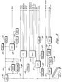
- the states of the signals under certain operating conditions are illustrated in accompanying Figures 4 and 5, which reference will be made.
- the signals originating from the storage controller 40 are known here as ACCEPT, FLUSH, ONE, TWO, and THREE.
- ACCEPT informs logical processors directly coupled to the local processor bus 34 (such as the microprocessor 32, maths coprocessor 39 and the bus interface controller 35) that there is either data or space available in the FIFO memory and that transfers can begin.
- ACCEPT is inactive (high in the accompanying Figures) where there is either not enough data or space to allow transfers.
- the storage controller 40 thus has the capability of signalling through the local processor bus 4 the availability of one of the blocks of data stored in the FIFO memory for transfer and space in the FIFO memory for reception of blocks of data to be transmitted.
- FLUSH informs the local processor bus logic that there is a need to remove all data stored in the FIFO memory, and is used only when data is being transferred from the FIFO memory to the local processor bus. FLUSH will remain active (low in the accompanying Figures) until all data is transferred out of the FIFO memory.
- the storage controller also has the capability of signalling through the local processor bus occurrences of storage of at least two predetermined different numbers of blocks of data to be delivered to said local processor bus. This capability is provided by the signals ONE, TWO and THREE. ONE informs the local processor bus logic that there is one byte of data left in the FIFO memory. ONE is used when data is transferred from the FIFO memory to the system, and allows the system to determine if a byte transfer only is required. TWO informs the local processor bus logic that there are two bytes of data left in the FIFO memory and is used when data is transferrd from the FIFO memory to the system.
- the TWO signal allows the local processor bus logic to determine whether enough data exits for a word transfer (a "word" being two bytes) or if pipelining operation can continue for one more cycle.
- THREE is used similarly to ONE and TWO, to indicate that there are three bytes of data in the FIFO memory for transfer to the system. If THREE is active, then the local processor bus logic allows pipelining operation to continue.
- the signals originating from the local processor bus logic are here known as ACK, HBV and LBV.
- the ACK signal is an acknowledgement, and informs the FIFO memory that data is being transferred.
- the HBV and LBV signals are used to signal through the local processor bus which portion of a block of data is to be considered valid. Assuming for present purposes that the block of data is a word of two bytes, then the HBV and LBV signals are indicative of the validity (or usefulness) of the entirety of a block of data (a word), a first half of a block of data (a byte), and a second half of a block of data (a byte).
- ACK goes active indicating a data transfer (as it will at the beginning of each transfer)
- the storage controller 40 must determined from HBV and LBV the amount of data to be transferred and which portion is to be deemed valid.
- Transfer of data from the FIFO memory to the system will begin either with ACCEPT going active or with FLUSH going active ( Figure 5).
- ACK will go active at the beginning of each transfer.
- HBV and LBV will indicate word or byte transfers, and which portion (if less than a word) is to be considered valid.
- the signals ONE, TWO and THREE are used to determine the transfer of data and whether pipelining can be continued.
- FLUSH goes inactive. If ACCEPT initiates the transfer rather than FLUSH, then ACCEPT will become inactive once a threshold level of fill has been reached, and the transfer of data will stop with the last cycle started.
Abstract
This invention relates to computers, and more particularly to a storage controller for a computer. The small computer systems interface (SCSI) controller is coupled directly to the local processor bus for controlling data transfer with storage memory devices such as fixed or removable media electromagnetic storage devices. The personal computer 10 system has a high speed local processor data bus 34, at least one logical processor device 32 coupled directly to the local processor bus 34 and capable of signalling through the local processor bus 34 an occurrence of the transfer of blocks of data, and a storage controller 40 coupled directly to the local processor bus 34 for regulating communications between the processor device 32 and storage memory devices 36. The storage controller 40 has a FIFO memory for transitory storage of blocks of data being exchanged with the local processor bus 34 and is capable of signalling through the local processor bus 34 the state of the FIFO memory. The processor device 32 and storage controller 40 cooperate for exchange of blocks of data between the local processor bus 34 and FIFO memory when the FIFO memory has available one of data to be transferred and space for reception of data and for emptying of the FIFO memory through the local processor bus 34 as necessary.
Description
- This invention relates to computers, and more particularly to a storage controller for a computer. The small computer systems interface (SCSI) controller is coupled directly to a local processor bus for controlling data transfer with storage devices such as fixed or removable media electromagnetic storage devices.
- Personal computer systems in general, and IBM personal computers in particular, have attained widespread use for providing computer power to many segments of today's modern society. Personal computer systems can usually be defined as desk top, floor standing, or portable microcomputers that consist of a system unit having a single system processor and associated volatile and non-volatile memory, a display monitor, a keyboard, one or more diskette drives, a fixed disk storage, and an optional printer. One of the distinguishing characteristics of these systems is the use of a motherboard or system planar to electrically connect these components together. These systems are designed primarily to give independent computing power to a single user and are inexpensively priced for purchase by individuals or small businesses. Examples of such personal computer systems are IBM's PERSONAL COMPUTER AT and IBM's PERSONAL SYSTEM/2 Models 25, 30, L40SX, 50, 55, 65, 70, 80, 90 and 95 (IBM, Personal Computer AT and Personal System/2 are registered trademarks of International Business Machines Corporation).
- These systems can be classified into two general families. The first family, usually referred to as Family I Models, use a bus architecture exemplified by the IBM PERSONAL COMPUTER AT and other "IBM compatible" machines. The second family, referred to as Family II Models, use IBM's MICRO CHANNEL (registered trademark of IBM) bus architecture exemplified by IBM's PERSONAL SYSTEM/2
Models 50 through 95. The Family I models typically have used the popular INTEL 8088 or 8086 microprocessor as the system processor. These processors have the ability to address one megabyte of memory. The Family II models typically use the high speed INTEL 80286, 80386, and 80486 microprocessors which can operate in a real mode to emulate the slower speed INTEL 8086 microprocessor or a protected mode which extends the addressing range from 1 megabyte to 4 Gigabytes for some models. In essence, the real mode feature of the 80286, 80386, and 80486 processors provide hardware compatibility with software written for the 8086 and 8088 microprocessors. - As the development of personal computer has advanced, there have been proposals for certain standards to be established among makers and users of such apparatus for the purpose of enabling greater exchangeability of components and the like. One such standard which has achieved some broad acceptance is the small computer systems interface (SCSI) standard for data communication to and from storage memory devices. For the present purposes, "storage memory devices" is defined broadly to include all devices capable of storing data in digital form, with particular emphasis on such devices as fixed or removable media electromagnetic storage devices (also known as hard and floppy disk drives), electro-optical, tape and other storage devices. SCSI controllers have been known and user prior to this invention, and will be familiar to the knowledgeable reader.
- In prior personal computer systems, SCSI controllers have typically been arranged as option or accessory devices, accessed by the system through the accessory or input/output or I/O bus. It is now contemplated to provide a SCSI controller as a single very large scale integrated (VLSI) device or application specific integrated circuit (ASIC) chip, and to provide for connection of that controller with a local processor bus. The purpose of so providing such a controller is to achieve enhanced performance in terms of expedited data transfers.
- Prior SCSI controllers have used a type of memory known as first in, first out (or FIFO), which may be provided by a series of registers. Communication with FIFO memory has been accomplished by a variety of arrangements such as moving a set of bytes of data at a time, or using acknowledge signals as data is moved. Such communication is complicated by direct coupling of a SCSI controller to a local processor bus, where new demands for data transfer control arise.
- The invention provides a computer comprising a high speed local processor data bus; at least one logical processor device coupled directly to the local processor bus, the processor device being capable of signalling through the local processor bus an occurrence of the transfer of blocks of data; and a storage controller coupled directly to the local processor bus for regulating communications between the processor device and storage memory devices, the storage controller having FIFO memory for transitory storage of blocks of data being exchanged with the local processor bus and being capable of signalling through the local processor bus the state of the FIFO memory; the processor device and the storage controller cooperating for exchange of blocks of data between the local processor bus and the FIFO memory when the FIFO memory has available one of data to be transferred and space for reception of data and for emptying of the FIFO memory through the local processor bus as necessary.
- Preferably the storage controller is capable of signalling through the local processor bus the availability of one of blocks of data stored in the FIFO memory for transfer and space in the FIFO memory for reception of blocks of data to be transferred and is capable of recognising signals passed through the local processor bus and indicative of an occurrence of the transfer of data and of which portion of a block of data is to be considered valid and is also capable of recognising signals passed through the local processor bus and indicative of an occurrence of the transfer of data and of which portion of a block of data is to be considered valid and of signalling through the local processor bus occurrences of storage of at least two predetermined different numbers of blocks of data to be delivered to the local processor bus.
- Preferably the processor device is capable of signalling through the local processor bus which portion of a block of data is to be considered valid and is capable of distinguishing between signals from the storage controller indicative of numbers of blocks of data to be delivered and of adapting the processing of data to the numbers of blocks indicated as to be delivered.
- Preferably the processor device and the storage controller are capable of distinguishing among signalled validity of the entirety of a block of data, a first half of a block of data, and a second half of a block of data.
- The invention will now be described, by way of example only, with reference to the accompanying drawings, in which:
- Figure 1 is a perspective view of a personal computer system embodying this invention;
- Figure 2 is an exploded perspective view of the microcomputer of the personal computer system of Figure 1;
- Figure 3 is a schematic view of the microcomputer of Figure 2;
- Figure 4 is a diagram of certain signals exchanged between a local processor bus and SCSI controller in the microcomputer of Figure 3; and
- Figure 5 is a diagram similar to Figure 4 illustrating certain other signals exchanged between a local processor bus and SCSI controller in the microcomputer of Figure 3.
- Figure 1 shows a
microcomputer 10 embodying the present invention. Themicrocomputer 10 may have an associated monitor 11,keyboard 12 and printer or plotter 14. Themicrocomputer 10 in Figure 2 has acover 15 which cooperates with achassis 19 in defining an enclosed, shielded volume for receiving electrically powered data processing and storage components for processing and storing digital data. At least certain of these components are mounted on amultilayer planar 20 or motherhoard which is mounted on thechassis 19 and provides a means for electrically interconnecting the components of themicrocomputer 10 including those identified above and such other associated elements as floppy disk drives, various forms of direct access storage devices, accessory cards or boards, and the like. - The
chassis 19 has a base and a rear panel (Figure 2) and defines at least one open bag for receiving a data storage device such as a disk drive for magnetic or optical disks, a tape backup drive, or the like. In the illustrated form, anupper bag 22 is adapted to receive peripheral drives of a first size (such as those known as 3.5 inch drives). A floppy disk drive, a removable media direct access storage device capable of receiving a diskette inserted thereinto and using the diskette to receive, store and deliver data as is generally known, may be provided in theupper bag 22. - Figure 3 is a block diagram of a
microcomputer 10 illustrating the various components, including components mounted on theplanar 20 and the connection of the planar to the I/O slots and other hardware of the personal computer system. Connected to the planar is the system processor (also known as CPU) 32. While any appropriate microprocessor can be used as theCPU 32, one suitable microprocessor is the 80386 which is sold by INTEL. Other suitable microprocessor include the INTEL 80286 or 80486 microprocessors. TheCPU 32 is connected by a high speed CPUlocal bus 34 to a businterface control unit 35, to volatile random access memory (RAM) 36 here shown as Single Inline Memory Modules (SIMMs) and toBIOS ROM 38 in which is stored instructions for basic input/output operations to theCPU 32. TheBIOS ROM 38 includes the BIOS that is used to interface between the I/O devices and the operating system of themicroprocessor 32. Instructions stored inROM 38 can be copied intoRAM 36 to decrease the execution time of BIOS. - The CPU local bus 34 (comprising data, address and control components) also provides for the connection of the
microprocessor 32 with amath coprocessor 39 and a storage controller 40. The storage controller 40 used in the embodiment of Figure 3 is a Small Computer Systems Interface (SCSI) controller which may, as is known to persons skilled in the arts of computer design and operation, be connected or connectable with Read Only Memory (ROM) 41,RAM 42, and suitable external devices of a variety of types as facilitated by the I/O connection indicated to the right in the Figure 3. The SCSI controller 40 functions as a storage controller in controlling storage memory devices such as fixed or removable media electromagnetic storage devices (also known as hard and floppy disk drives), electro-optical, tape and other storage devices. - The bus interface controller (BIC) 35 couples the CPU
local bus 34 with an I/O bus 44. By means of thebus 44, the BIG 35 is coupled with an optional feature bus as a MICRO CHANNEL bus having a plurality of I/O slots for receiving MICRO CHANNELadapter cards 45 which may be further connected to an I/O device or memory (not shown). The I/O bus 44 includes address, data, and control components. - Coupled along the I/
O bus 44 are a variety of I/O components such as avideo signal processor 46 which is associated with video RAM (VRAM) for storing graphic information (indicated at 48) and for storing image information (indicated at 49). Video signals exchanged with theprocessor 46 may be passed through a Digital to Analog Converter (DAC) 50 to a monitor or other display device. Provision is also made for connecting theVSP 46 directly with what is here referred to as a natural image input/output, which may take the form of a video recorder/player, camera, etc. The I/O bus 44 is also coupled with a Digital Signal Processor (DSP) 51 which has associatedinstruction RAM 52 anddata RAM 54 available to store software instructions for the processing of signals by the DSP 51 and data involved in such processing. The DSP 51 provides for processing of audio inputs and outputs by the provision of anaudio controller 55, and for handling of other signals by provision of ananalog interface controller 56. Lastly, the I/O bus 44 is coupled with a input/output controller 58 with associated Electrical Erasable Programmable Read Only Memory (EEPROM) 59 by which inputs and outputs are exchanged with conventional peripherals including floppy disk drives, a printer or plotter 14,keyboard 12, a mouse or pointing device (not shown), and by means of a serial port. - In order to provide for effective data transfer between the
local processor bus 34 and the storage controller 40 and particularly a FIFO memory included within the controller 40, the present invention defines certain handshaking protocol signals. The exchange of these signals over thelocal processor bus 34 prevents overrun of the FIFO memory and underrun to the local processor bus, and allow the local processor bus to go into pipeline operation mode without the loss of data integrity and the FIFO memory to pass data while avoiding corruption of the data. The states of the signals under certain operating conditions are illustrated in accompanying Figures 4 and 5, which reference will be made. - The signals originating from the storage controller 40 are known here as ACCEPT, FLUSH, ONE, TWO, and THREE. ACCEPT informs logical processors directly coupled to the local processor bus 34 (such as the
microprocessor 32,maths coprocessor 39 and the bus interface controller 35) that there is either data or space available in the FIFO memory and that transfers can begin. ACCEPT is inactive (high in the accompanying Figures) where there is either not enough data or space to allow transfers. The storage controller 40 thus has the capability of signalling through the local processor bus 4 the availability of one of the blocks of data stored in the FIFO memory for transfer and space in the FIFO memory for reception of blocks of data to be transmitted. FLUSH informs the local processor bus logic that there is a need to remove all data stored in the FIFO memory, and is used only when data is being transferred from the FIFO memory to the local processor bus. FLUSH will remain active (low in the accompanying Figures) until all data is transferred out of the FIFO memory. - The storage controller also has the capability of signalling through the local processor bus occurrences of storage of at least two predetermined different numbers of blocks of data to be delivered to said local processor bus. This capability is provided by the signals ONE, TWO and THREE. ONE informs the local processor bus logic that there is one byte of data left in the FIFO memory. ONE is used when data is transferred from the FIFO memory to the system, and allows the system to determine if a byte transfer only is required. TWO informs the local processor bus logic that there are two bytes of data left in the FIFO memory and is used when data is transferrd from the FIFO memory to the system. The TWO signal allows the local processor bus logic to determine whether enough data exits for a word transfer (a "word" being two bytes) or if pipelining operation can continue for one more cycle. THREE is used similarly to ONE and TWO, to indicate that there are three bytes of data in the FIFO memory for transfer to the system. If THREE is active, then the local processor bus logic allows pipelining operation to continue.
- The signals originating from the local processor bus logic are here known as ACK, HBV and LBV. The ACK signal is an acknowledgement, and informs the FIFO memory that data is being transferred. The HBV and LBV signals are used to signal through the local processor bus which portion of a block of data is to be considered valid. Assuming for present purposes that the block of data is a word of two bytes, then the HBV and LBV signals are indicative of the validity (or usefulness) of the entirety of a block of data (a word), a first half of a block of data (a byte), and a second half of a block of data (a byte). When ACK goes active indicating a data transfer (as it will at the beginning of each transfer), the storage controller 40 must determined from HBV and LBV the amount of data to be transferred and which portion is to be deemed valid.
- Transfer of data to the FIFO memory from the system will begin with ACCEPT going active (Figure 4). ACK will go active at the beginning of each transfer, while HBV and LBV will indicate a word or byte transfer. Once the FIFO memory has reached a threshold level of fill, ACCEPT will be made inactive and the transfer of data will stop with the last cycle started.
- Transfer of data from the FIFO memory to the system will begin either with ACCEPT going active or with FLUSH going active (Figure 5). ACK will go active at the beginning of each transfer. HBV and LBV will indicate word or byte transfers, and which portion (if less than a word) is to be considered valid. The signals ONE, TWO and THREE are used to determine the transfer of data and whether pipelining can be continued. Once the last byte is transferred, FLUSH goes inactive. If ACCEPT initiates the transfer rather than FLUSH, then ACCEPT will become inactive once a threshold level of fill has been reached, and the transfer of data will stop with the last cycle started.
Claims (9)
- A computer 10 comprising:
a high speed local processor data bus 34;
at least one logical processor device 32 coupled directly to said local processor bus, said processor device being capable of signalling through said local processor bus 34 an occurrence of the transfer of blocks of data; and
a storage controller 40 coupled directly to said local processor bus 34 for regulating communications between said processor device 32 and storage memory devices 36, said storage controller having FIFO memory for transitory storage of blocks of data being exchanged with said local processor bus and being capable of signalling through said local processor bus the state of the FIFO memory;
said processor device 32 and said storage controller 40 cooperating for exchange of blocks of data between said local processor bus 34 and said FIFO memory when said FIFO memory has available one of data to be transferred and space for reception of data and for emptying of said FIFO memory through said local processor bus as necessary. - A computer 10 as claimed in claim 1 wherein said storage controller 40 is capable of signalling through said local processor bus 34 the availability of one of blocks of data stored in the FIFO memory for transfer and space, in the FIFO memory for reception of blocks of data to be transferred.
- A computer 10 as claimed in any preceding claim wherein said processor device 32 is capable of signalling through said local processor bus 34 which portion of a block of data is to be considered valid.
- A computer 10 as claimed in any preceding claim wherein said storage controller 40 is capable of recognising signals passes through said local processor bus 34 and indicative of an occurrence of the transfer of data and of which portion of a block of data is to be considered valid.
- A computer 10 as claimed in any preceding claim wherein said processor device 32 and said storage controller 40 are capable of distinguishing among signalled validity of the entirety of a block of data, a first half of a block of data, and a second half of a block of data.
- A computer 10 as claimed in any preceding claim wherein said storage controller 40 is capable of signalling through said local processor bus 34 occurrences of storage of at least two predetermined different numbers of blocks of data to be delivered to said local processor bus.
- A computer 10 as claimed in claim 6 wherein said processor device 32 is capable of distinguishing between signals from said storage controller 40 indicative of numbers of blocks of data to be delivered and of adapting the processing of data to the numbers of blocks indicated to be delivered.
- A computer 10 comprising:
a high speed local processor data bus 34;
at least one logical processor device 32 coupled directly to said local processor bus 34, said processor device being capable of signalling through said local processor bus an occurrence of the transfer of blocks of data and which portion of a block of data is to be considered valid; and
a storage controller 40 coupled directly to said local processor bus 34 for regulating communications between said processor device 32 and storage memory devices 36, said storage controller having FIFO memory for transitory storage of blocks of data being exchanged with said local processor bus and being capable of signalling through said local processor bus the availability of one of blocks of data stored in the FIFO memory for transfer and space in the FIFO memory for reception of blocks of data to be transferred, said storage controller also being capable of recognising signals passed through said local processor bus and indicative of an occurrence of the transfer of data and of which portion of a block of data is to be considered valid;
said processor device 32 and said storage controller 40 being capable of distinguishing among signalled validity of the entirety of a block of data, a first half of a block of data, and a second half of a block of data, and cooperating for exchange of blocks of data between said local processor bus and said FIFO memory when said FIFO memory has available one of data to be transferred and space for reception of data and for emptying of said FIFO memory through said local processor bus 34 as necessary. - A computer 10 as claimed in claim 8 wherein said storage controller 40 is capable of signalling through said local processor bus 34 occurrences of storage of at least two predetermined numbers of blocks of data to be delivered to said processor bus and wherein said processor device 32 is capable of distinguishing between signals from said storage controller indicative of numbers of blocks of data to be delivered and of adapting the processing of data to the numbers of blocks indicated to be delivered.
Applications Claiming Priority (2)
| Application Number | Priority Date | Filing Date | Title |
|---|---|---|---|
| US71223391A | 1991-06-07 | 1991-06-07 | |
| US712233 | 1991-06-07 |
Publications (1)
| Publication Number | Publication Date |
|---|---|
| EP0517509A1 true EP0517509A1 (en) | 1992-12-09 |
Family
ID=24861287
Family Applications (1)
| Application Number | Title | Priority Date | Filing Date |
|---|---|---|---|
| EP92305095A Withdrawn EP0517509A1 (en) | 1991-06-07 | 1992-06-03 | A computer including a storage controller |
Country Status (4)
| Country | Link |
|---|---|
| US (1) | US5550991A (en) |
| EP (1) | EP0517509A1 (en) |
| JP (1) | JPH05173954A (en) |
| CA (1) | CA2065989C (en) |
Families Citing this family (6)
| Publication number | Priority date | Publication date | Assignee | Title |
|---|---|---|---|---|
| US5649162A (en) * | 1993-05-24 | 1997-07-15 | Micron Electronics, Inc. | Local bus interface |
| US5719920A (en) * | 1995-03-31 | 1998-02-17 | The Messenger Group Llc | Method and apparatus for processing and downloading sound messages onto a permanent memory of a communication package |
| US5768162A (en) * | 1995-07-26 | 1998-06-16 | Comptek Federal Systems, Inc. | Data bus recorder |
| US6038620A (en) * | 1996-09-09 | 2000-03-14 | International Business Machines Corporation | Method and system for optimal high speed match in a high performance controller which ensures an input/output interface stays ahead of a host interface |
| US6006344A (en) * | 1997-01-21 | 1999-12-21 | Dell Usa, L.P., A Texas Limited Partnership | Keyboard controlled diagnostic system |
| US7716437B2 (en) * | 2007-07-31 | 2010-05-11 | International Business Machines Corporation | Dynamic timer configuration for task monitoring in a remote mirror and copy environment |
Citations (3)
| Publication number | Priority date | Publication date | Assignee | Title |
|---|---|---|---|---|
| EP0113683A2 (en) * | 1983-01-11 | 1984-07-18 | Unisys Corporation | Burst mode data block transfer system |
| EP0321157A2 (en) * | 1987-12-15 | 1989-06-21 | Advanced Micro Devices, Inc. | Direct memory access apparatus and methods |
| EP0410566A2 (en) * | 1989-06-19 | 1991-01-30 | International Business Machines Corporation | Data processing system with means to convert burst operations into pipelined operations |
Family Cites Families (16)
| Publication number | Priority date | Publication date | Assignee | Title |
|---|---|---|---|---|
| US4288860A (en) * | 1979-08-02 | 1981-09-08 | Sperry Corporation | Dynamic storage synchronizer using variable oscillator and FIFO buffer |
| US4344132A (en) * | 1979-12-14 | 1982-08-10 | International Business Machines Corporation | Serial storage interface apparatus for coupling a serial storage mechanism to a data processor input/output bus |
| US5038277A (en) * | 1983-11-07 | 1991-08-06 | Digital Equipment Corporation | Adjustable buffer for data communications in a data processing system |
| US4935894A (en) * | 1987-08-31 | 1990-06-19 | Motorola, Inc. | Multi-processor, multi-bus system with bus interface comprising FIFO register stocks for receiving and transmitting data and control information |
| US5175825A (en) * | 1990-02-02 | 1992-12-29 | Auspex Systems, Inc. | High speed, flexible source/destination data burst direct memory access controller |
| US5142626A (en) * | 1990-07-20 | 1992-08-25 | International Business Machines Corp. | Personal computer with removable media identification |
| US5440693A (en) * | 1990-07-19 | 1995-08-08 | International Business Machines Corp. | Personal computer with drive identification |
| US5265255A (en) * | 1990-09-24 | 1993-11-23 | International Business Machines Corp. | Personal computer system with interrupt controller |
| US5301343A (en) * | 1990-12-31 | 1994-04-05 | International Business Machines Corp. | System having microprocessor local memory expansion capability through removable coupling of local memory expansion boards directly to the high speed microprocessor local bus |
| US5353417A (en) * | 1991-05-28 | 1994-10-04 | International Business Machines Corp. | Personal computer with bus interface controller coupled directly with local processor and input/output data buses and for anticipating memory control changes on arbitration for bus access |
| US5287476A (en) * | 1991-06-07 | 1994-02-15 | International Business Machines Corp. | Personal computer system with storage controller controlling data transfer |
| US5371861A (en) * | 1992-09-15 | 1994-12-06 | International Business Machines Corp. | Personal computer with small computer system interface (SCSI) data flow storage controller capable of storing and processing multiple command descriptions ("threads") |
| US5299315A (en) * | 1992-09-17 | 1994-03-29 | International Business Machines Corp. | Personal computer with programmable threshold FIFO registers for data transfer |
| US5313593A (en) * | 1992-09-17 | 1994-05-17 | International Business Machines Corp. | Personal computer system with bus noise rejection |
| US5471585A (en) * | 1992-09-17 | 1995-11-28 | International Business Machines Corp. | Personal computer system with input/output controller having serial/parallel ports and a feedback line indicating readiness of the ports |
| US5485585A (en) * | 1992-09-18 | 1996-01-16 | International Business Machines Corporation | Personal computer with alternate system controller and register for identifying active system controller |
-
1992
- 1992-04-14 CA CA002065989A patent/CA2065989C/en not_active Expired - Fee Related
- 1992-05-11 JP JP4117726A patent/JPH05173954A/en active Pending
- 1992-06-03 EP EP92305095A patent/EP0517509A1/en not_active Withdrawn
-
1995
- 1995-03-28 US US08/411,916 patent/US5550991A/en not_active Expired - Fee Related
Patent Citations (3)
| Publication number | Priority date | Publication date | Assignee | Title |
|---|---|---|---|---|
| EP0113683A2 (en) * | 1983-01-11 | 1984-07-18 | Unisys Corporation | Burst mode data block transfer system |
| EP0321157A2 (en) * | 1987-12-15 | 1989-06-21 | Advanced Micro Devices, Inc. | Direct memory access apparatus and methods |
| EP0410566A2 (en) * | 1989-06-19 | 1991-01-30 | International Business Machines Corporation | Data processing system with means to convert burst operations into pipelined operations |
Non-Patent Citations (1)
| Title |
|---|
| RESEARCH DISCLOSURE. no. 309, January 1990, NEW YORK US page 11; 'method of handling odd byte transfers on small computer system interface controllers' * |
Also Published As
| Publication number | Publication date |
|---|---|
| JPH05173954A (en) | 1993-07-13 |
| CA2065989A1 (en) | 1992-12-08 |
| US5550991A (en) | 1996-08-27 |
| CA2065989C (en) | 1998-03-31 |
Similar Documents
| Publication | Publication Date | Title |
|---|---|---|
| US5299315A (en) | Personal computer with programmable threshold FIFO registers for data transfer | |
| US5371861A (en) | Personal computer with small computer system interface (SCSI) data flow storage controller capable of storing and processing multiple command descriptions ("threads") | |
| US5265255A (en) | Personal computer system with interrupt controller | |
| US5020999A (en) | Personal computer with connector assembly having integral retainer | |
| US5734840A (en) | PCI and expansion bus riser card | |
| US5276864A (en) | Personal computer with alternate system controller error detection | |
| EP0493888A2 (en) | Personal computer with local memory expansion capability | |
| JP2970081B2 (en) | Personal computer for identifying drive mechanism | |
| US5287476A (en) | Personal computer system with storage controller controlling data transfer | |
| US5550991A (en) | Personal computer system having high speed local processor bus and storage controller with FIFO memory coupled directly thereto | |
| US5485585A (en) | Personal computer with alternate system controller and register for identifying active system controller | |
| US5293590A (en) | Personal computer with interface controller | |
| US5537600A (en) | Personal computer with alternate system controller | |
| CA2066001C (en) | Personal computer memory write control | |
| US5630078A (en) | Personal computer with processor reset control | |
| EP0588469A1 (en) | Personal computer with SCSI bus power control | |
| EP0516323A1 (en) | Personal computer systems | |
| EP0517415A1 (en) | Personal computer with enhanced memory access and method | |
| JPH05128055A (en) | Personal computer system having alternate- system controlling apparatus |
Legal Events
| Date | Code | Title | Description |
|---|---|---|---|
| PUAI | Public reference made under article 153(3) epc to a published international application that has entered the european phase |
Free format text: ORIGINAL CODE: 0009012 |
|
| AK | Designated contracting states |
Kind code of ref document: A1 Designated state(s): DE FR GB IT |
|
| 17P | Request for examination filed |
Effective date: 19930427 |
|
| 17Q | First examination report despatched |
Effective date: 19970923 |
|
| STAA | Information on the status of an ep patent application or granted ep patent |
Free format text: STATUS: THE APPLICATION IS DEEMED TO BE WITHDRAWN |
|
| 18D | Application deemed to be withdrawn |
Effective date: 19980204 |