US4935894A - Multi-processor, multi-bus system with bus interface comprising FIFO register stocks for receiving and transmitting data and control information - Google Patents
Multi-processor, multi-bus system with bus interface comprising FIFO register stocks for receiving and transmitting data and control information Download PDFInfo
- Publication number
- US4935894A US4935894A US07/091,675 US9167587A US4935894A US 4935894 A US4935894 A US 4935894A US 9167587 A US9167587 A US 9167587A US 4935894 A US4935894 A US 4935894A
- Authority
- US
- United States
- Prior art keywords
- bus
- data
- processor
- coupled
- control information
- Prior art date
- Legal status (The legal status is an assumption and is not a legal conclusion. Google has not performed a legal analysis and makes no representation as to the accuracy of the status listed.)
- Expired - Fee Related
Links
Images


Classifications
-
- G—PHYSICS
- G06—COMPUTING; CALCULATING OR COUNTING
- G06F—ELECTRIC DIGITAL DATA PROCESSING
- G06F13/00—Interconnection of, or transfer of information or other signals between, memories, input/output devices or central processing units
- G06F13/38—Information transfer, e.g. on bus
- G06F13/40—Bus structure
- G06F13/4004—Coupling between buses
- G06F13/4027—Coupling between buses using bus bridges
Definitions
- This invention relates generally to the area of digital data processing systems and, in particular, to the interfacing of two different asynchronous bus-based computer systems.
- IBM 3270 System A first well-known type of computer system, commonly referred to as an IBM 3270 System, has found wide-spread commercial use in applications such as data entry, word processing, transaction-handling, data communications, etc. There are many known types of IBM and IBM-compatible 3270 systems in use by nearly all of the Fortune 1000 companies.
- an IBM 3270 System comprises a plurality of IBM 3270 terminals coupled to an IBM host processor by means of an IBM 3274 controller. Both the host processor and the controller are coupled to a system bus known as an IBM Multibus.
- IBM Multibus a system bus known as an IBM Multibus.
- the structure and functionality of the IBM Multibus conform to a uniquely defined bus specification with respect to a wide variety of bus parameters such as the number and width of channels, bus timing, parity, etc.
- the IBM 3270 terminals are coupled to the IBM 3274 controller by means of two-conductor, twisted-pair coaxial cables referred to as RG62 cables.
- RG62 cables two-conductor, twisted-pair coaxial cables.
- IBM 3270 Systems installed throughout the world, there is also a very large quantity of IBM 3270 terminals.
- coaxial cable coupling such IBM 3270 terminals to their respective IBM 3274 controllers The current rate for installation of RG62 cabling is approximately $10-25 per linear foot.
- the UNIX operating system supports improvements in development software, application software, and distributed data processing software which are not available using the IBM 3270 System alone.
- certain commercially available processors operating under the UNIX operating systems represent the leading edge in processor versatility and throughput.
- VME bus is a widely used standard bus.
- processors and associated memory and peripheral equipment are compatible with the VME bus, and they are commercially available from many different vendors worldwide. Much of this equipment cannot be connected to the IBM Multibus.
- IBM 3274 controller does not support many types of printers and data storage devices. It currently supports only dot matrix and line printers. Thus, it would be very desirable if there were a way to connect new varieties of peripheral equipment to IBM 3274 controllers operating on the IBM Multibus.
- a circuit for interfacing between an IBM 3270 system and a VME system is required to achieve the above-described functionality. More specifically a circuit for interfacing the asynchronous IBM Multibus and the asynchronous VME bus is required.
- a known prior art circuit for interfacing two different data processing systems operated by locking the two different system buses together. Whenever one system bus was in use, operations on the other system bus had to be halted until the first system bus was again free. This had a significantly adverse effect on the operation of both computer systems. There is thus a significant need for an interface between two different asynchronous system buses having the features described above, in which each system bus can operate independently of the other.
- the present invention pertains to a multi-processor, multi-bus system which utilizes a pair of bus interface circuits between two different computer systems having first and second bus types to enable users of either computer system to access either system.
- Each bus interface circuit comprises a first-in-first-out (FIFO) register stack, interrupt logic, and transmitter/receiver logic.
- FIFO first-in-first-out
- the pair of bus interface circuits provides dual simplex data and control transfer between the two buses.
- the data and command transfer between processors in the system is accomplished by a protocol which utilizes a fixed 16-bit wide format control word.
- the most significant bit 15, referred to as a command bit is a "one" whenever bits 0-7 contain a command byte, while the command bit is "zero" whenever bits 0-7 contain a data byte.
- a logical unit number specified in bits 8-14 indicates to which of 128 possible logical devices the information transfer is destined to go.
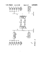
- FIG. 1 is a block diagram of a multi-processor, multi-bus system having an interface embodying the present invention
- FIG. 2 is a more detailed block diagram of the bus A and bus B interfaces illustrated in FIG. 1;
- FIG. 3 is a detailed block diagram of the bus A interface illustrated in FIG. 1;
- FIG. 4 is a detailed block diagram of the bus B interface illustrated in FIG. 1;
- FIG. 5 is an illustration of the format of a 16-bit control word used in the present invention.
- FIG. 6 is an illustration of a multi-byte data transfer block used in the present invention.
- System 10 has two asynchronous buses 12 and 14.
- Bus 12 has coupled to it a processor 16 and a device controller 18.
- a series of peripheral units 21-25 are coupled to and controlled by device controller 18.
- Peripheral units 21-25 may be work stations, printers, and the like.
- processor 16 is a standard Intel processor
- controller 18 is a specialized controller for IBM coax-A devices
- at least one of peripheral units 21-25 are IBM Model 3270 terminals. It will be understood that plug-compatible units may be substituted for IBM units.
- Bus 14 has a processor 20 and a series of peripheral units 31-35 coupled to it.
- Processor 20 is of a different type than processor 16.
- processor 20 is a Motorola 68020 processor running under the UNIX operating system, and at least one of peripheral units 31-35 is a terminal unit.
- bus interface 40 associated with bus 12
- bus interface 50 associated with bus 14.
- a dual simplex path for data and control information is created by buses 42 and 44.
- a dual simplex path is a path wherein information is transferred between two elements in one direction along one line connecting them, and simultaneously in the opposite direction along a second line connecting them.
- bus 42 transfers data and control information from bus interface 50 to bus interface 40, while bus 44 transfers data and control information from bus interface 40 to bus interface 50.
- Bus interfaces 40 and 50 allow peripheral units 21-25 to access processor 20, and they also allow peripheral units 31-35 to access processor 16. This functionality of system 10 is achieved while keeping the operation of buses 12 and 14 independent and will be described in greater detail in succeeding paragraphs.
- peripheral units 21-25 have been shown connected through controller 18 to bus 12, and peripheral units 31-35 have been shown connected to bus 14, these elements are not essential to the present invention. Situations may arise where two types of processors are required to be joined, but no peripheral units are necessary on one bus or the other. Furthermore, while five peripheral units have been shown attached to each bus in FIG. 1 for illustrative purposes, more or less peripheral units are possible.
- Bus interface 40 includes interrupt and control logic 46 and a FIFO register stack 55. Associated with FIFO register stack 55 is a status register 59.
- Bus interface 50 includes interrupt and control logic 48 and a FIFO register stack 60. Associated with FIFO register stack 60 is a status register 61.
- a dual simplex path for data and control information is achieved by interconnecting buses 42 and 44.
- FIFO register stack 55 receives data from bus 14 via data bus 57, drivers 88, data and control bus 42, and line receivers 56 and transfers it to bus 12
- FIFO register stack 55 receives control information from bus 14 via address and control bus 54, interrupt and control logic 48, control bus 42, drivers 88, data and control bus 42, and line receivers 56.
- FIFO register stack 55 and drivers 98 also receive control information over control bus 41 via line receivers 56, bus 46, and interrupt and control logic 46.
- FIFO register stack 60 receives data from bus 12 via data bus 53, drivers 98, data and control bus 44, and line receivers 86 and transfers it to bus 14.
- FIFO register stack 60 receives control information from bus 12 via address and control bus 52, interrupt and control logic 46, control bus 41, drivers 98, data and control bus 44, and line receivers 86.
- FIFO register stack 60 and drivers 88 also receive control information over control bus 42 via line receivers 86, bus 43, and interrupt and control logic 48.
- address and control information is generated bi-directionally along bus 52 between interrupt and control logic 46 bus 12, and along bus 54 between interrupt and control logic 48 and bus 14. This assures synchronism between the functioning of bus 12 and bus 14.
- FIG. 3 A detailed block diagram of bus interface 40 appearing between bus 12 and buses 42 and 44 is illustrated in FIG. 3.
- Line receivers 56 receive data and control information from bus 42. Control information is passed to control logic means 64 via line 70, and data information is transferred through bus 69 to FIFO register stack 55.
- Bus 69 is 16-bits wide. If FIFO register stack 55 is a 512 ⁇ 18 register stack, two bits in each line of FIFO register 55 are ignored. Also, a predetermined number of lines in FIFO register stack 55 acts as a buffer.
- FIFO register stack 55 serves as a read FIFO register if a READ signal is supplied on line 71 from control logic means 64.
- FIFO register stack 55 serves as a write register stack if a WRITE signal is supplied on line 73.
- a WRITE signal on line 73 would be generated from control logic means 94 of the bus B interface 50 (See FIG. 4).
- FIFO register stack 55 has a status register 59 to indicate the level of data information in the part of FIFO register stack 55 which is being utilized as a buffer. If the buffer is full, a FULL FLAG signal indicating this is sent along line 74 to control logic means 94 of the bus B interface; if the buffer is half full, a HALF FULL signal is generated along line 76 to interrupt control means 62; and, if the buffer is empty an EMPTY signal is generated along line 75 to control logic means 64 and interrupt control means 62.
- FIFO register stacks 55 and 60 can be any of several commercially available parts with the required functions such as Integrated Device Technology Part No. IDT7201.
- Interrupt control means 62 sends control signals to processor 16 through bus 77 and bus logic 65.
- Bus logic 65 controls and correlates information flowing from bus 12 to other elements in the system.
- Board select logic 68 controls bus logic board 65 by means of bus 67.
- FIFO 55 has a data output bus 66 for sending data either to bus 12 (through bus logic 65) or to line drivers 58.
- bus logic 95 differs slightly from bus logic 65, since it must interface with bus 14 which is of a different type than bus 12.
- Control word 120 is used as part of a parallel data link (PDL) protocol for the transfer of commands and data between processor 16 and processor 20.
- PDL parallel data link
- the PDL protocol enables up to 128 logical devices to be logically connected in the system.
- the PDL protocol supports two kinds of transfers: data transfers and command transfers. Data transfers can be either single-byte data transfers or multi-byte data transfers.
- the most significant bit (MSB) 15 of control word 120 labeled as a command bit 121, is a logical "one" whenever bits 0 through 7 contain a valid command byte 123.
- the command bit is a logical "zero" when bits 121 0 through 7 contain a valid data byte 123.
- a logical unit number 122 contained in bits 8 through 14 specifies the logical device to which the transfer is destined to go. Since the logical unit number 122 comprises seven bits, the logical unit number 122 has a range of 0 to 127.
- bits 0 through 7 of control word 120 contain a Command Byte (if bit 15 is set) or a Data Byte (if bit 15 is not set) for the logical device specified in bits 8 through 14.
- data transfers can be either multi-byte or single-byte in nature.
- the choice of which type of transfer to use is determined by many system design considerations. One such consideration is the amount of data that is to be transferred. If there are four or fewer bytes to transfer, single-byte data transfer is more efficient. However, if there are five or more bytes to transfer, multi-byte data transfer is utilized.
- Single-byte data transfers are accomplished by placing the data byte 123 to be transferred in bits 0 through 7 of control word 120, placing the logical unit number 122 in bits 8 through 14, and clearing the command bit 121 to "zero".
- Multi-byte data transfer really begins with a command transfer.
- a multi-byte data transfer block 110 is illustrated in FIG. 6.
- the first word 111 in multi-byte data transfer block 110 is a control word which contains a C - MB - DATA command byte (see Appendix) in bits 0 through 7, a logical unit number in bits 8 through 14, and a "one" in the command bit position.
- the second word 112 of multibyte data transfer block 110 contains a count of the number of data bytes to follow.
- the third and subsequent word, collectively labeled 113 contain the actual data bytes to be transferred.
- the number of bytes in words 113 correspond to the data byte count designated in word 112. Even-numbered data bytes are placed in bits 8 through 15, and odd-numbered data bytes are placed in bits 0 through 7. If the transfer contains an odd number of bytes, it may be advantageous to have the last of words 113 contain "zeros" in bits 0 through 7 to indicate that the last data byte has been transferred.
- control word 120 By using the format specified in FIG. 6, data and command transfer occur between processors 16 and 20 along a dual simplex path. While a specific format for control word 120 has been described, it should be apparent to those skilled in the art that variations are possible. For instance, the least significant bit (LSB) of control word 120 could be the command bit if specified as such, etc.
- LSB least significant bit
- the interface circuit of the present invention when used to interface two different types of computer systems, a user on either system can utilize a processor and/or peripheral equipment associated with either computer system. Efficient functioning is maintained although the buses are asynchronous due to the status, control and interrupt functions of the interfaces.
- Data and control transfers are performed between different processors in the overall system according to a protocol which transmits information regarding whether a transfer represents data or a command, which logical unit the transfer is destined to go to, and the specific data or command.
- the Appendix provides detailed information regarding bus addressing, interrupt operations, status register operations, bus logic control functions, and command transfers of the present invention. Specific address codes have been omitted, since this will vary depending on the type of bus utilized.
Landscapes
- Engineering & Computer Science (AREA)
- General Engineering & Computer Science (AREA)
- Theoretical Computer Science (AREA)
- Computer Hardware Design (AREA)
- Physics & Mathematics (AREA)
- General Physics & Mathematics (AREA)
- Bus Control (AREA)
Abstract
Description
              APPENDIX
______________________________________
BUS ADDRESSING:
READ    WRITE       FUNCTION
______________________________________
X                   Read FIFO data
        X           Write FIFO data
        X           Enable interrupts
        X           Disable interrupts
X                   Generate Reset
        X           Load interrupt Mask Register
        X           Clear interrupt 4
                    (other CPU reset)
        X           Clear interrupt 3
                    (write buffer full)
        X           Clear interrupt 2
                    (write buffer empty)
        X           Clear interrupt 1
                    (write buffer 1/2 full)
        X           Clear interrupt 0
                    (receive character available)
X                   Read status register
                    (valid lower 8 bits only)
______________________________________
INTERRUPT OPERATIONS:
I0    Set by the FIFO, serving as a read FIFO
      register, when there is a character present. I0
      will be held until the CLEAR interrupt 0 command
      is issued.
I1    Set by the FIFO, serving as a write FIFO
      register, reaching the HALF FULL level. I1 will
      remain on until the CLEAR interrupt 1 command is
      issued.
I2    Set by the FIFO, serving as a write FIFO
      register, reaching the EMPTY state. I2 will be
      held until the CLEAR interrupt 2 command is
      issued.
I3    Set by the FIFO, serving as a write FIFO
      register, reaching the FULL state. I3 will be
      held on until the CLEAR interrupt 3 command is
      issued. -I4 Set when the RESET level is applied to the other
      CPU. I4 will be held as long as the other
      system reset is asserted. When the other system
      reset is de-asserted, the interrupt will be
      cleared.
STATUS REGISTER OPERATION:
S0    This is an unlatched signal which represents the
      actual current condition of the FIFO serving as
      a read FIFO register.
0 =      The FIFO is empty.
1 =      The FIFO has an entry.
S1    A latched signal indicating that the FIFO has
      been filled to the one-half plus 1 entry level.
1 =      The FIFO is half full.
         The bit can be reset by clearing
         interrupt 1.
S2    A latched signal indicating that the FIFO
      serving as a write FIFO register has been
      emptied.
1 =      FIFO is empty.
         This bit can be reset by clearing
         interrupt 2.
S3    Latched signal indicating the FIFO serving as a
      write FIFO register has been completely filled.
1 =      FIFO is full.
         This bit can be reset by clearing
         interrupt 3.
S4    Latched signal indicating the other CPU has done
      a RESET.
1 =      System holding RESET TRUE.
         This bit can be reset by clearing
         interrupt 4. If the reset is still being
         held true, the bit will not reset.
S5    local (read) FIFO full flag (low true, not
      latched)
S6    local (read) FIFO full flag (low true, not
      latched)
S7    Summary Bit
1 =      One or more of the Interrupt bits is set.
         Note that the Empty indicator (S0) is  .sub.----not
         latched, but the word present [NOT EMPTY]
         (I0)  .sub.--is latched and reflected in S7. Hence
         the interrupt status may not represent
         current status of the FIFO.
BUS LOGIC CONTROL FUNCTIONS:
FIFO        Reading this address retrieves a
READ        16 bit word from the onboard (local) FIFO
            if a word is available.
FIFO        Writing this address transfers a 16 bit
WRITE       word to the FIFO on the mating interface
            card (remote FIFO) if it is not full. If
            the FIFO is full, nothing will be written
            nor will any error be indicated! Use the
            FIFO full interrupt or the status register
            to avoid this condition.
ENABLE      Writing to this location enable the OR
INTERRUPTS  of interrupts (I0-I4) to be applied to
            onboard I2. Data is not significant for
            this instruction.
DISABLE     Writing to this location disables the
INTERRUPTS  interrupts from the bus. Interrupt status
            is not changed, but is only de-asserted
            from the onboard bus. Data is not
            significant for this operation.
RESET       Reading the RESET address on the logic
            board will set interrupts I0 thru I4 to all
            1's and reset both FIFO's (FIFO Data is
             ------LOST).
            The Enable/Disable condition of both
            system's interrupt is not affected. A
RESET       state signifies an ABORT with
            possible data loss. No data is returned by
            this command.
WRITE       Writing an 8-bit byte to the interrupt
INTERRUPT   mask register address allows bits to be
MASK        sent to the logic board to enable/mask
REGISTER    the individual interrupts I0-I3. An "0"
            bit in the register will mask  --on the
            corresponding interrupt. A "1" bit in the
            register will mask  --off the corresponding
            interrupt as follows:
          BIT0 I0
                 BIT4 NOT USED
          BIT1 I1
                 BIT5 NOT USED
          BIT2 I2
                 BIT6 NOT USED
          BIT3 I3
                 BIT7 NOT USED
CLEAR       Writing this address will clear
I4          interrupt I4, which would have been set by
            a hard reset or a reset command. Data is
            not significant with this command.
CLEAR       Writing to this address will clear
I3          interrupt I3 which would have been set by
            the write (remote) FIFO reaching the full
            state. This interrupt could also have been
            set by a hard or soft system reset. Data
            is not significant with this command.
CLEAR       Writing to this address will clear
I2          interrupt I2 which would have been set by
            the write (remote) FIFO reaching the
            empty state. A hard or soft reset will also
            set this interrupt true. Data is not
            significant with this command.
CLEAR       Writing to this address will clear
I1          interrupt I1 which would have been set by
            the write (remote) FIFO reaching the half
            full state. A hard or soft reset will also
            set this interrupt true. Data is not
            significant with this command.
CLEAR       Writing to this address will clear
I0          interrupt I0 which would have been set by
            the read (local) FIFO reaching the data
            available state. A hard or soft reset will
            also set this interrupt true. Data is not
            significant with this command.
READ        Reading this address will return
STATUS      the logic board's status in the
REGISTER    lower 8 bits of the word. The upper 8 bits
            are not driven by the board and will
            probably be FF hex.
COMMAND TRANSFERS:
C --RESET   This command is used to reset the PDL
            interface. It may be issued by either side
            of the interface.
C --ONLINE  This command is used to signal device
            availability. It may be issued by either
            side of the interface.
C --OFFLINE This command is used whenever a device has
            become unavailable.
C --SACT    This command is used whenever a device
            which was temporarily unavailable (see
            C --SINACT, below) has returned to ser-
            vice. C --SACT may be issued by either side of the
            interface.
C --SINACT  This command is used whenever a device
            becomes temporarily unavailable, usually
            due to the device switching to an alternate
            session. C --SINACT may be issued by
            either side of the interface.
C --SEND    This command (in conjunction with
            C --STOP) provides device level flow con-
            trol. C --SEND may be issued by either
            side of the interface.
C --STOP    This command (in conjunction with
            C --SEND) provides device level flow con-
            trol. C --STOP may be issued by
            either side of the interface.
C --MB --DATA
            This command signifies the start of a
            Multibyte Data Transfer.
C --FT --START
            This command indicates the beginning of
            File Transfer Mode.
C --FT --STOP
            This command terminates File Transfer Mode.
C --FT --RESEND
            This command is used to request
            retransmission of the last File Transfer
            data block.
C --ALARM   This command is used to indicate that data
            is present for the logical unit but the
            logical unit is presently inactive (see
            C --SINACT, above).
C --LU --DSP
            This command is used to configure the
            logical unit as an ASCII display device.
C --LU --PRT
            This command is used to configure the
            logical unit as an ASCII print device.
C --LU --DECONF
            This command is used to deconfigure
            ASCII display and printer devices.
C --MB --ACK
            This command is used to acknowledge the
            receipt of a Multi-byte Data Transfer
            command. It may be sent by either side of
            the interface when it is determined that
            enough buffer space exists to receive
            another multi-byte data transfer.
C --NOP     The C --NOP command is used to send a
            dummy command. It may be sent by either
            side of the interface.
C --CMD --REJ
            The C --CMD --REJ command is used
            whenever the last command received for
            device is logically incorrect
            (eg: sending C --SEND when the logical
            unit is not blocked, etc.) It may be sent
            by either side of the interface.
C --LU --RESET
            The C --LU --RESET command resets
            a specific port.
C --BREAK   The C --BREAK command signals the
            coordinated processor to emulate the pro-
            cessing required to break the transmission.
______________________________________
Claims (8)
Priority Applications (1)
| Application Number | Priority Date | Filing Date | Title |
|---|---|---|---|
| US07/091,675 US4935894A (en) | 1987-08-31 | 1987-08-31 | Multi-processor, multi-bus system with bus interface comprising FIFO register stocks for receiving and transmitting data and control information |
Applications Claiming Priority (1)
| Application Number | Priority Date | Filing Date | Title |
|---|---|---|---|
| US07/091,675 US4935894A (en) | 1987-08-31 | 1987-08-31 | Multi-processor, multi-bus system with bus interface comprising FIFO register stocks for receiving and transmitting data and control information |
Publications (1)
| Publication Number | Publication Date |
|---|---|
| US4935894A true US4935894A (en) | 1990-06-19 |
Family
ID=22229081
Family Applications (1)
| Application Number | Title | Priority Date | Filing Date |
|---|---|---|---|
| US07/091,675 Expired - Fee Related US4935894A (en) | 1987-08-31 | 1987-08-31 | Multi-processor, multi-bus system with bus interface comprising FIFO register stocks for receiving and transmitting data and control information |
Country Status (1)
| Country | Link |
|---|---|
| US (1) | US4935894A (en) |
Cited By (92)
| Publication number | Priority date | Publication date | Assignee | Title |
|---|---|---|---|---|
| EP0490573A1 (en) * | 1990-12-07 | 1992-06-17 | Digital Equipment Corporation | Method and apparatus for providing high performance interconnection between information buses |
| EP0524684A2 (en) * | 1991-07-22 | 1993-01-27 | International Business Machines Corporation | A universal buffered interface for coupling multiple processors, memory units, and I/O interfaces to a common high-speed bus |
| US5191581A (en) * | 1990-12-07 | 1993-03-02 | Digital Equipment Corporation | Method and apparatus for providing high performance interconnection between interface circuits coupled to information buses |
| WO1993004432A2 (en) * | 1991-08-16 | 1993-03-04 | Multichip Technology | High-performance dynamic memory system |
| US5218690A (en) * | 1989-06-08 | 1993-06-08 | Bull Hn Information Systems Inc. | Vme-multibus ii interface adapter for protocol conversion and for monitoring and discriminating accesses on the multibus ii system bus |
| US5222227A (en) * | 1987-01-16 | 1993-06-22 | Hitachi, Ltd. | Direct memory access controller for a multi-microcomputer system |
| US5226124A (en) * | 1991-06-05 | 1993-07-06 | Ambrosia Microcomputer Products, Inc. | Communication interface between a radio control transmitter and a computer data bus |
| WO1993019422A1 (en) * | 1992-03-25 | 1993-09-30 | Encore Computer U.S., Inc. | Fiber optic memory coupling system |
| US5280584A (en) * | 1989-11-21 | 1994-01-18 | Deutsche Itt Industries Gmbh | Two-way data transfer apparatus |
| US5287464A (en) * | 1990-10-24 | 1994-02-15 | Zilog, Inc. | Semiconductor multi-device system with logic means for controlling the operational mode of a set of input/output data bus drivers |
| US5335326A (en) * | 1992-10-01 | 1994-08-02 | Xerox Corporation | Multichannel FIFO device channel sequencer |
| US5363485A (en) * | 1992-10-01 | 1994-11-08 | Xerox Corporation | Bus interface having single and multiple channel FIFO devices using pending channel information stored in a circular queue for transfer of information therein |
| US5423049A (en) * | 1991-01-31 | 1995-06-06 | Nec Corporation | Multiprocessor circuit |
| US5428801A (en) * | 1989-02-28 | 1995-06-27 | Sharp Kabushiki Kaisha | Data array conversion control system for controlling conversion of data arrays being transferred between two processing systems |
| US5442754A (en) * | 1992-12-04 | 1995-08-15 | Unisys Corporation | Receiving control logic system for dual bus network |
| US5450547A (en) * | 1992-10-01 | 1995-09-12 | Xerox Corporation | Bus interface using pending channel information stored in single circular queue for controlling channels of data transfer within multiple FIFO devices |
| US5499338A (en) * | 1990-12-19 | 1996-03-12 | Motorola, Inc. | Bus system having a system bus, an internal bus with functional units coupled therebetween and a logic unit for use in such system |
| US5511165A (en) * | 1992-10-23 | 1996-04-23 | International Business Machines Corporation | Method and apparatus for communicating data across a bus bridge upon request |
| US5519883A (en) * | 1993-02-18 | 1996-05-21 | Unisys Corporation | Interbus interface module |
| US5544331A (en) * | 1993-09-30 | 1996-08-06 | Silicon Graphics, Inc. | System and method for generating a read-modify-write operation |
| US5548785A (en) * | 1990-03-30 | 1996-08-20 | International Business Machines Corporation | Interface for logic simulation using parallel bus for concurrent transfers and having fifo buffers for sending data to receiving units when ready |
| US5550991A (en) * | 1991-06-07 | 1996-08-27 | International Business Machines Corporation | Personal computer system having high speed local processor bus and storage controller with FIFO memory coupled directly thereto |
| US5555543A (en) * | 1995-01-03 | 1996-09-10 | International Business Machines Corporation | Crossbar switch apparatus and protocol |
| US5581732A (en) * | 1984-03-10 | 1996-12-03 | Encore Computer, U.S., Inc. | Multiprocessor system with reflective memory data transfer device |
| US5584040A (en) * | 1992-10-20 | 1996-12-10 | Cirrus Logic, Inc. | High performance peripheral interface with read-ahead capability |
| US5590349A (en) * | 1988-07-11 | 1996-12-31 | Logic Devices, Inc. | Real time programmable signal processor architecture |
| WO1997000480A1 (en) * | 1995-06-15 | 1997-01-03 | Intel Corporation | Architecture for an i/o processor that integrates a pci to pci bridge |
| US5592684A (en) * | 1994-07-22 | 1997-01-07 | Dell Usa, L.P. | Store queue including a byte order tracking mechanism for maintaining data coherency |
| US5594874A (en) * | 1993-09-30 | 1997-01-14 | Cirrus Logic, Inc. | Automatic bus setting, sensing and switching interface unit |
| US5608877A (en) * | 1995-03-24 | 1997-03-04 | Cirrus Logic, Inc. | Reset based computer bus identification method and circuit resilient to power transience |
| US5619653A (en) * | 1992-09-04 | 1997-04-08 | Nec Corporation | Buffer device with resender |
| US5655112A (en) * | 1992-10-23 | 1997-08-05 | International Business Machines Corporation | Method and apparatus for enabling data paths on a remote bus |
| WO1997034235A1 (en) * | 1996-03-13 | 1997-09-18 | Diamond Multimedia Systems, Inc. | Multi-threaded fifo pool buffer and bus transfer control system |
| US5687396A (en) * | 1989-12-04 | 1997-11-11 | Canon Kabushiki Kaisha | Data buffer apparatus with interrupted transmission/reception |
| US5692200A (en) * | 1995-10-16 | 1997-11-25 | Compaq Computer Corporation | Bridge circuit for preventing data incoherency by holding off propagation of data transfer completion interrupts until data clears the bridge circuit |
| US5699529A (en) * | 1990-08-31 | 1997-12-16 | Ncr Corporation | Work station or similar data processing system including interfacing means to a data channel |
| US5717932A (en) * | 1994-11-04 | 1998-02-10 | Texas Instruments Incorporated | Data transfer interrupt pacing |
| US5727184A (en) * | 1994-06-27 | 1998-03-10 | Cirrus Logic, Inc. | Method and apparatus for interfacing between peripherals of multiple formats and a single system bus |
| US5729708A (en) * | 1989-12-04 | 1998-03-17 | Canon Kabushiki Kaisha | Portable data buffer apparatus with manually controlled reception/transmission |
| US5754866A (en) * | 1995-05-08 | 1998-05-19 | Nvidia Corporation | Delayed interrupts with a FIFO in an improved input/output architecture |
| US5768550A (en) * | 1995-11-21 | 1998-06-16 | International Business Machines Corporation | Bus interface logic system |
| US5794014A (en) * | 1994-06-27 | 1998-08-11 | Cirrus Logic, Inc. | Method and apparatus for interfacing between peripherals of multiple formats and a single system bus |
| US5797043A (en) * | 1996-03-13 | 1998-08-18 | Diamond Multimedia Systems, Inc. | System for managing the transfer of data between FIFOs within pool memory and peripherals being programmable with identifications of the FIFOs |
| US5835970A (en) * | 1995-12-21 | 1998-11-10 | Cypress Semiconductor Corp. | Burst address generator having two modes of operation employing a linear/nonlinear counter using decoded addresses |
| US5933613A (en) * | 1995-07-06 | 1999-08-03 | Hitachi, Ltd. | Computer system and inter-bus control circuit |
| US5931926A (en) * | 1995-07-07 | 1999-08-03 | Sun Microsystems, Inc. | Method and apparatus for dynamically calculating degrees of fullness of a synchronous FIFO |
| GB2334415A (en) * | 1998-02-13 | 1999-08-18 | Motorola Ltd | Interfacing multiplexed and non- multiplexed busses |
| US5943509A (en) * | 1997-06-27 | 1999-08-24 | Nec Corporation | Small size inter-processor data transfer system |
| US6012108A (en) * | 1996-06-29 | 2000-01-04 | Samsung Electronics Co., Ltd. | Device for dualizing main processors in an asynchronous transfer mode switch and method therefor |
| US6049887A (en) * | 1997-12-04 | 2000-04-11 | Intel Corporation | Method and apparatus for propagating a signal between synchronous clock domains operating at a non-integer frequency ratio |
| US6098113A (en) * | 1992-10-22 | 2000-08-01 | Ncr Corporation | Apparatus and method for address translation and allocation for a plurality of input/output (I/O) buses to a system bus |
| US6173374B1 (en) * | 1998-02-11 | 2001-01-09 | Lsi Logic Corporation | System and method for peer-to-peer accelerated I/O shipping between host bus adapters in clustered computer network |
| US6286067B1 (en) | 1999-09-21 | 2001-09-04 | Sony Corporation | Method and system for the simplification of leaf-limited bridges |
| US6374316B1 (en) | 1999-03-19 | 2002-04-16 | Sony Corporation | Method and system for circumscribing a topology to form ring structures |
| US6502158B1 (en) | 1999-04-23 | 2002-12-31 | Sony Corporation | Method and system for address spaces |
| US6539450B1 (en) | 1998-11-29 | 2003-03-25 | Sony Corporation | Method and system for adjusting isochronous bandwidths on a bus |
| US6560573B1 (en) * | 1999-07-30 | 2003-05-06 | Emc Corporation | Storage controller with hardware emulation controller for emulation between control processor and transfer circuitry compatible to different processor |
| US6584539B1 (en) | 1999-03-19 | 2003-06-24 | Sony Corporation | Method and system for message broadcast flow control on a bus bridge interconnect |
| US20030172206A1 (en) * | 2002-03-05 | 2003-09-11 | Stacey Secatch | Pushback fifo |
| US6631415B1 (en) | 1999-03-19 | 2003-10-07 | Sony Corporation | Method and system for providing a communication connection using stream identifiers |
| US6647446B1 (en) | 2000-03-18 | 2003-11-11 | Sony Corporation | Method and system for using a new bus identifier resulting from a bus topology change |
| US20040022204A1 (en) * | 2002-07-31 | 2004-02-05 | Matthew Trembley | Full duplex/half duplex serial data bus adapter |
| US6728821B1 (en) | 1999-11-29 | 2004-04-27 | Sony Corporation | Method and system for adjusting isochronous bandwidths on a bus |
| US6757762B1 (en) | 1999-10-29 | 2004-06-29 | Unisys Corporation | Multi-mode processor bus bridge |
| US6757773B1 (en) | 2000-06-30 | 2004-06-29 | Sony Corporation | System and method for determining support capability of a device coupled to a bus system |
| US6772257B1 (en) * | 1999-12-23 | 2004-08-03 | Intel Corporation | Method and apparatus for processing interrupts |
| US6810452B1 (en) | 1999-03-19 | 2004-10-26 | Sony Corporation | Method and system for quarantine during bus topology configuration |
| US20040260858A1 (en) * | 2001-07-31 | 2004-12-23 | Primrose Donald R. | Configurable glueless microprocessor interface |
| US20040260832A1 (en) * | 2003-06-23 | 2004-12-23 | Newisys, Inc., A Delaware Corporation | Bandwidth, framing and error detection in communications between multi-processor clusters of multi-cluster computer systems |
| US20050034033A1 (en) * | 2003-08-05 | 2005-02-10 | Newisys, Inc. | Communication between and within multi-processor clusters of multi-cluster computer systems |
| DE10350388A1 (en) * | 2003-10-28 | 2005-06-02 | Micronas Gmbh | Bus system with few control lines |
| US20060047754A1 (en) * | 2002-11-15 | 2006-03-02 | Infineon Technologies Ag | Mailbox interface between processors |
| US20100146225A1 (en) * | 2008-12-10 | 2010-06-10 | Georg Biehler | Acyclic data transfer via a field bus coupler |
| US9749548B2 (en) | 2015-01-22 | 2017-08-29 | Google Inc. | Virtual linebuffers for image signal processors |
| US9756268B2 (en) | 2015-04-23 | 2017-09-05 | Google Inc. | Line buffer unit for image processor |
| US9769356B2 (en) | 2015-04-23 | 2017-09-19 | Google Inc. | Two dimensional shift array for image processor |
| US9772852B2 (en) | 2015-04-23 | 2017-09-26 | Google Inc. | Energy efficient processor core architecture for image processor |
| US9785423B2 (en) | 2015-04-23 | 2017-10-10 | Google Inc. | Compiler for translating between a virtual image processor instruction set architecture (ISA) and target hardware having a two-dimensional shift array structure |
| US9830150B2 (en) | 2015-12-04 | 2017-11-28 | Google Llc | Multi-functional execution lane for image processor |
| CN107533458A (en) * | 2016-02-04 | 2018-01-02 | 慧与发展有限责任合伙企业 | The signaling and message transmission interrupted based on memory register |
| US9965824B2 (en) | 2015-04-23 | 2018-05-08 | Google Llc | Architecture for high performance, power efficient, programmable image processing |
| US9978116B2 (en) | 2016-07-01 | 2018-05-22 | Google Llc | Core processes for block operations on an image processor having a two-dimensional execution lane array and a two-dimensional shift register |
| US9986187B2 (en) | 2016-07-01 | 2018-05-29 | Google Llc | Block operations for an image processor having a two-dimensional execution lane array and a two-dimensional shift register |
| US10095479B2 (en) | 2015-04-23 | 2018-10-09 | Google Llc | Virtual image processor instruction set architecture (ISA) and memory model and exemplary target hardware having a two-dimensional shift array structure |
| US10204396B2 (en) | 2016-02-26 | 2019-02-12 | Google Llc | Compiler managed memory for image processor |
| US10284744B2 (en) | 2015-04-23 | 2019-05-07 | Google Llc | Sheet generator for image processor |
| US10313641B2 (en) | 2015-12-04 | 2019-06-04 | Google Llc | Shift register with reduced wiring complexity |
| US10380969B2 (en) | 2016-02-28 | 2019-08-13 | Google Llc | Macro I/O unit for image processor |
| US10387989B2 (en) | 2016-02-26 | 2019-08-20 | Google Llc | Compiler techniques for mapping program code to a high performance, power efficient, programmable image processing hardware platform |
| US10546211B2 (en) | 2016-07-01 | 2020-01-28 | Google Llc | Convolutional neural network on programmable two dimensional image processor |
| US10885996B2 (en) | 1997-10-08 | 2021-01-05 | Pact Xpp Schweiz Ag | Processor having a programmable function unit |
| US10915773B2 (en) | 2016-07-01 | 2021-02-09 | Google Llc | Statistics operations on two dimensional image processor |
Citations (12)
| Publication number | Priority date | Publication date | Assignee | Title |
|---|---|---|---|---|
| US4205373A (en) * | 1978-05-22 | 1980-05-27 | Ncr Corporation | System and method for accessing memory connected to different bus and requesting subsystem |
| US4234919A (en) * | 1978-10-31 | 1980-11-18 | Honeywell Information Systems Inc. | Intersystem communication link |
| US4263649A (en) * | 1979-01-05 | 1981-04-21 | Mohawk Data Sciences Corp. | Computer system with two busses |
| US4309754A (en) * | 1979-07-30 | 1982-01-05 | International Business Machines Corp. | Data interface mechanism for interfacing bit-parallel data buses of different bit width |
| US4319338A (en) * | 1979-12-12 | 1982-03-09 | Allen-Bradley Company | Industrial communications network with mastership determined by need |
| US4422142A (en) * | 1979-06-22 | 1983-12-20 | Fujitsu Fanuc Limited | System for controlling a plurality of microprocessors |
| US4451886A (en) * | 1980-04-30 | 1984-05-29 | Hewlett-Packard Limited | Bus extender circuitry for data transmission |
| US4456994A (en) * | 1979-01-31 | 1984-06-26 | U.S. Philips Corporation | Remote simulation by remote control from a computer desk |
| US4625307A (en) * | 1984-12-13 | 1986-11-25 | United Technologies Corporation | Apparatus for interfacing between at least one channel and at least one bus |
| US4698753A (en) * | 1982-11-09 | 1987-10-06 | Texas Instruments Incorporated | Multiprocessor interface device |
| US4723238A (en) * | 1986-03-24 | 1988-02-02 | American Telephone And Telegraph Company | Interface circuit for interconnecting circuit switched and packet switched systems |
| US4744023A (en) * | 1985-12-16 | 1988-05-10 | American Telephone And Telegraph Company, At&T Information Systems | Processor access control arrangement in a multiprocessor system |
-
1987
- 1987-08-31 US US07/091,675 patent/US4935894A/en not_active Expired - Fee Related
Patent Citations (12)
| Publication number | Priority date | Publication date | Assignee | Title |
|---|---|---|---|---|
| US4205373A (en) * | 1978-05-22 | 1980-05-27 | Ncr Corporation | System and method for accessing memory connected to different bus and requesting subsystem |
| US4234919A (en) * | 1978-10-31 | 1980-11-18 | Honeywell Information Systems Inc. | Intersystem communication link |
| US4263649A (en) * | 1979-01-05 | 1981-04-21 | Mohawk Data Sciences Corp. | Computer system with two busses |
| US4456994A (en) * | 1979-01-31 | 1984-06-26 | U.S. Philips Corporation | Remote simulation by remote control from a computer desk |
| US4422142A (en) * | 1979-06-22 | 1983-12-20 | Fujitsu Fanuc Limited | System for controlling a plurality of microprocessors |
| US4309754A (en) * | 1979-07-30 | 1982-01-05 | International Business Machines Corp. | Data interface mechanism for interfacing bit-parallel data buses of different bit width |
| US4319338A (en) * | 1979-12-12 | 1982-03-09 | Allen-Bradley Company | Industrial communications network with mastership determined by need |
| US4451886A (en) * | 1980-04-30 | 1984-05-29 | Hewlett-Packard Limited | Bus extender circuitry for data transmission |
| US4698753A (en) * | 1982-11-09 | 1987-10-06 | Texas Instruments Incorporated | Multiprocessor interface device |
| US4625307A (en) * | 1984-12-13 | 1986-11-25 | United Technologies Corporation | Apparatus for interfacing between at least one channel and at least one bus |
| US4744023A (en) * | 1985-12-16 | 1988-05-10 | American Telephone And Telegraph Company, At&T Information Systems | Processor access control arrangement in a multiprocessor system |
| US4723238A (en) * | 1986-03-24 | 1988-02-02 | American Telephone And Telegraph Company | Interface circuit for interconnecting circuit switched and packet switched systems |
Non-Patent Citations (2)
| Title |
|---|
| "CMOS Parallel First-In/First-Out FIFO 512×9 Bit & 1024×9 Bit", Military and Commercial Temperature Ranges, pp. 2-34-2-42. |
| CMOS Parallel First In/First Out FIFO 512 9 Bit & 1024 9 Bit , Military and Commercial Temperature Ranges, pp. 2 34 2 42. * |
Cited By (152)
| Publication number | Priority date | Publication date | Assignee | Title |
|---|---|---|---|---|
| US5581732A (en) * | 1984-03-10 | 1996-12-03 | Encore Computer, U.S., Inc. | Multiprocessor system with reflective memory data transfer device |
| US5222227A (en) * | 1987-01-16 | 1993-06-22 | Hitachi, Ltd. | Direct memory access controller for a multi-microcomputer system |
| US5590349A (en) * | 1988-07-11 | 1996-12-31 | Logic Devices, Inc. | Real time programmable signal processor architecture |
| US5428801A (en) * | 1989-02-28 | 1995-06-27 | Sharp Kabushiki Kaisha | Data array conversion control system for controlling conversion of data arrays being transferred between two processing systems |
| US5218690A (en) * | 1989-06-08 | 1993-06-08 | Bull Hn Information Systems Inc. | Vme-multibus ii interface adapter for protocol conversion and for monitoring and discriminating accesses on the multibus ii system bus |
| US5280584A (en) * | 1989-11-21 | 1994-01-18 | Deutsche Itt Industries Gmbh | Two-way data transfer apparatus |
| US5687396A (en) * | 1989-12-04 | 1997-11-11 | Canon Kabushiki Kaisha | Data buffer apparatus with interrupted transmission/reception |
| US5729708A (en) * | 1989-12-04 | 1998-03-17 | Canon Kabushiki Kaisha | Portable data buffer apparatus with manually controlled reception/transmission |
| US5548785A (en) * | 1990-03-30 | 1996-08-20 | International Business Machines Corporation | Interface for logic simulation using parallel bus for concurrent transfers and having fifo buffers for sending data to receiving units when ready |
| US5699529A (en) * | 1990-08-31 | 1997-12-16 | Ncr Corporation | Work station or similar data processing system including interfacing means to a data channel |
| US5287464A (en) * | 1990-10-24 | 1994-02-15 | Zilog, Inc. | Semiconductor multi-device system with logic means for controlling the operational mode of a set of input/output data bus drivers |
| US5191581A (en) * | 1990-12-07 | 1993-03-02 | Digital Equipment Corporation | Method and apparatus for providing high performance interconnection between interface circuits coupled to information buses |
| EP0490573A1 (en) * | 1990-12-07 | 1992-06-17 | Digital Equipment Corporation | Method and apparatus for providing high performance interconnection between information buses |
| US5499338A (en) * | 1990-12-19 | 1996-03-12 | Motorola, Inc. | Bus system having a system bus, an internal bus with functional units coupled therebetween and a logic unit for use in such system |
| US5423049A (en) * | 1991-01-31 | 1995-06-06 | Nec Corporation | Multiprocessor circuit |
| US5226124A (en) * | 1991-06-05 | 1993-07-06 | Ambrosia Microcomputer Products, Inc. | Communication interface between a radio control transmitter and a computer data bus |
| US5550991A (en) * | 1991-06-07 | 1996-08-27 | International Business Machines Corporation | Personal computer system having high speed local processor bus and storage controller with FIFO memory coupled directly thereto |
| US5870572A (en) * | 1991-07-22 | 1999-02-09 | International Business Machines Corporation | Universal buffered interface for coupling multiple processors, memory units, and I/O interfaces to a common high-speed interconnect |
| US5588122A (en) * | 1991-07-22 | 1996-12-24 | International Business Machines Corporation | Universal buffered interface for coupling multiple processors memory units, and I/O interfaces to a common high-speed interconnect |
| EP0524684A3 (en) * | 1991-07-22 | 1994-02-16 | Ibm | |
| EP0524684A2 (en) * | 1991-07-22 | 1993-01-27 | International Business Machines Corporation | A universal buffered interface for coupling multiple processors, memory units, and I/O interfaces to a common high-speed bus |
| US5781918A (en) * | 1991-08-16 | 1998-07-14 | Cypress Semiconductor Corp. | Memory system and method for selecting a different number of data channels depending on bus size |
| WO1993004432A3 (en) * | 1991-08-16 | 1993-04-15 | Multichip Technology | High-performance dynamic memory system |
| US5469558A (en) * | 1991-08-16 | 1995-11-21 | Multichip Technology | Dynamically reconfigurable memory system with programmable controller and FIFO buffered data channels |
| WO1993004432A2 (en) * | 1991-08-16 | 1993-03-04 | Multichip Technology | High-performance dynamic memory system |
| US5544319A (en) * | 1992-03-25 | 1996-08-06 | Encore Computer U.S., Inc. | Fiber optic memory coupling system with converter transmitting and receiving bus data in parallel fashion and diagnostic data in serial fashion |
| WO1993019422A1 (en) * | 1992-03-25 | 1993-09-30 | Encore Computer U.S., Inc. | Fiber optic memory coupling system |
| US5619653A (en) * | 1992-09-04 | 1997-04-08 | Nec Corporation | Buffer device with resender |
| US5450547A (en) * | 1992-10-01 | 1995-09-12 | Xerox Corporation | Bus interface using pending channel information stored in single circular queue for controlling channels of data transfer within multiple FIFO devices |
| US5335326A (en) * | 1992-10-01 | 1994-08-02 | Xerox Corporation | Multichannel FIFO device channel sequencer |
| US5363485A (en) * | 1992-10-01 | 1994-11-08 | Xerox Corporation | Bus interface having single and multiple channel FIFO devices using pending channel information stored in a circular queue for transfer of information therein |
| US5592682A (en) * | 1992-10-20 | 1997-01-07 | Cirrus Logic, Inc. | Interface circuit for transferring data between host device and mass storage device in response to designated address in host memory space assigned as data port |
| US5826107A (en) * | 1992-10-20 | 1998-10-20 | Cirrus Logic, Inc. | Method and apparatus for implementing a DMA timeout counter feature |
| US6131132A (en) * | 1992-10-20 | 2000-10-10 | Cirrus Logic, Inc. | High performance peripheral interface |
| US5655145A (en) * | 1992-10-20 | 1997-08-05 | Cirrus Logic, Inc. | Peripheral interface circuit which snoops commands to determine when to perform DMA protocol translation |
| US5603052A (en) * | 1992-10-20 | 1997-02-11 | Cirrus Logic, Inc. | Interface circuit for transferring data between host and mass storage by assigning address in the host memory space and placing the address on the bus |
| US5584040A (en) * | 1992-10-20 | 1996-12-10 | Cirrus Logic, Inc. | High performance peripheral interface with read-ahead capability |
| US5630171A (en) * | 1992-10-20 | 1997-05-13 | Cirrus Logic, Inc. | Translating from a PIO protocol to DMA protocol with a peripheral interface circuit |
| US6098113A (en) * | 1992-10-22 | 2000-08-01 | Ncr Corporation | Apparatus and method for address translation and allocation for a plurality of input/output (I/O) buses to a system bus |
| US5655112A (en) * | 1992-10-23 | 1997-08-05 | International Business Machines Corporation | Method and apparatus for enabling data paths on a remote bus |
| US5511165A (en) * | 1992-10-23 | 1996-04-23 | International Business Machines Corporation | Method and apparatus for communicating data across a bus bridge upon request |
| US5442754A (en) * | 1992-12-04 | 1995-08-15 | Unisys Corporation | Receiving control logic system for dual bus network |
| US5519883A (en) * | 1993-02-18 | 1996-05-21 | Unisys Corporation | Interbus interface module |
| US5544331A (en) * | 1993-09-30 | 1996-08-06 | Silicon Graphics, Inc. | System and method for generating a read-modify-write operation |
| US5594874A (en) * | 1993-09-30 | 1997-01-14 | Cirrus Logic, Inc. | Automatic bus setting, sensing and switching interface unit |
| US5794014A (en) * | 1994-06-27 | 1998-08-11 | Cirrus Logic, Inc. | Method and apparatus for interfacing between peripherals of multiple formats and a single system bus |
| US5727184A (en) * | 1994-06-27 | 1998-03-10 | Cirrus Logic, Inc. | Method and apparatus for interfacing between peripherals of multiple formats and a single system bus |
| US5905885A (en) * | 1994-06-27 | 1999-05-18 | Cirrus Logic, Inc. | Method and apparatus for interfacing between peripherals of multiple formats and a single system bus |
| US5592684A (en) * | 1994-07-22 | 1997-01-07 | Dell Usa, L.P. | Store queue including a byte order tracking mechanism for maintaining data coherency |
| US5717932A (en) * | 1994-11-04 | 1998-02-10 | Texas Instruments Incorporated | Data transfer interrupt pacing |
| US5555543A (en) * | 1995-01-03 | 1996-09-10 | International Business Machines Corporation | Crossbar switch apparatus and protocol |
| US5608877A (en) * | 1995-03-24 | 1997-03-04 | Cirrus Logic, Inc. | Reset based computer bus identification method and circuit resilient to power transience |
| US5754866A (en) * | 1995-05-08 | 1998-05-19 | Nvidia Corporation | Delayed interrupts with a FIFO in an improved input/output architecture |
| WO1997000480A1 (en) * | 1995-06-15 | 1997-01-03 | Intel Corporation | Architecture for an i/o processor that integrates a pci to pci bridge |
| US5884027A (en) * | 1995-06-15 | 1999-03-16 | Intel Corporation | Architecture for an I/O processor that integrates a PCI to PCI bridge |
| US5933613A (en) * | 1995-07-06 | 1999-08-03 | Hitachi, Ltd. | Computer system and inter-bus control circuit |
| US5931926A (en) * | 1995-07-07 | 1999-08-03 | Sun Microsystems, Inc. | Method and apparatus for dynamically calculating degrees of fullness of a synchronous FIFO |
| US5692200A (en) * | 1995-10-16 | 1997-11-25 | Compaq Computer Corporation | Bridge circuit for preventing data incoherency by holding off propagation of data transfer completion interrupts until data clears the bridge circuit |
| US5768550A (en) * | 1995-11-21 | 1998-06-16 | International Business Machines Corporation | Bus interface logic system |
| US5835970A (en) * | 1995-12-21 | 1998-11-10 | Cypress Semiconductor Corp. | Burst address generator having two modes of operation employing a linear/nonlinear counter using decoded addresses |
| US5797043A (en) * | 1996-03-13 | 1998-08-18 | Diamond Multimedia Systems, Inc. | System for managing the transfer of data between FIFOs within pool memory and peripherals being programmable with identifications of the FIFOs |
| US5784649A (en) * | 1996-03-13 | 1998-07-21 | Diamond Multimedia Systems, Inc. | Multi-threaded FIFO pool buffer and bus transfer control system |
| WO1997034235A1 (en) * | 1996-03-13 | 1997-09-18 | Diamond Multimedia Systems, Inc. | Multi-threaded fifo pool buffer and bus transfer control system |
| US6012108A (en) * | 1996-06-29 | 2000-01-04 | Samsung Electronics Co., Ltd. | Device for dualizing main processors in an asynchronous transfer mode switch and method therefor |
| US5943509A (en) * | 1997-06-27 | 1999-08-24 | Nec Corporation | Small size inter-processor data transfer system |
| AU734501B2 (en) * | 1997-06-27 | 2001-06-14 | Nec Platforms, Ltd. | Small size inter-processor data transfer system |
| US10885996B2 (en) | 1997-10-08 | 2021-01-05 | Pact Xpp Schweiz Ag | Processor having a programmable function unit |
| US6049887A (en) * | 1997-12-04 | 2000-04-11 | Intel Corporation | Method and apparatus for propagating a signal between synchronous clock domains operating at a non-integer frequency ratio |
| US6173374B1 (en) * | 1998-02-11 | 2001-01-09 | Lsi Logic Corporation | System and method for peer-to-peer accelerated I/O shipping between host bus adapters in clustered computer network |
| GB2334415A (en) * | 1998-02-13 | 1999-08-18 | Motorola Ltd | Interfacing multiplexed and non- multiplexed busses |
| US6539450B1 (en) | 1998-11-29 | 2003-03-25 | Sony Corporation | Method and system for adjusting isochronous bandwidths on a bus |
| US6631415B1 (en) | 1999-03-19 | 2003-10-07 | Sony Corporation | Method and system for providing a communication connection using stream identifiers |
| US6584539B1 (en) | 1999-03-19 | 2003-06-24 | Sony Corporation | Method and system for message broadcast flow control on a bus bridge interconnect |
| US6374316B1 (en) | 1999-03-19 | 2002-04-16 | Sony Corporation | Method and system for circumscribing a topology to form ring structures |
| US6810452B1 (en) | 1999-03-19 | 2004-10-26 | Sony Corporation | Method and system for quarantine during bus topology configuration |
| US6502158B1 (en) | 1999-04-23 | 2002-12-31 | Sony Corporation | Method and system for address spaces |
| US6560573B1 (en) * | 1999-07-30 | 2003-05-06 | Emc Corporation | Storage controller with hardware emulation controller for emulation between control processor and transfer circuitry compatible to different processor |
| US6286067B1 (en) | 1999-09-21 | 2001-09-04 | Sony Corporation | Method and system for the simplification of leaf-limited bridges |
| US6757762B1 (en) | 1999-10-29 | 2004-06-29 | Unisys Corporation | Multi-mode processor bus bridge |
| US6728821B1 (en) | 1999-11-29 | 2004-04-27 | Sony Corporation | Method and system for adjusting isochronous bandwidths on a bus |
| US6772257B1 (en) * | 1999-12-23 | 2004-08-03 | Intel Corporation | Method and apparatus for processing interrupts |
| US6647446B1 (en) | 2000-03-18 | 2003-11-11 | Sony Corporation | Method and system for using a new bus identifier resulting from a bus topology change |
| US6757773B1 (en) | 2000-06-30 | 2004-06-29 | Sony Corporation | System and method for determining support capability of a device coupled to a bus system |
| US20040260858A1 (en) * | 2001-07-31 | 2004-12-23 | Primrose Donald R. | Configurable glueless microprocessor interface |
| US6842816B1 (en) * | 2001-07-31 | 2005-01-11 | Network Elements, Inc. | Configurable glueless microprocessor interface |
| USRE40660E1 (en) * | 2001-07-31 | 2009-03-10 | Primrose Donald R | Configurable glueless microprocessor interface |
| US20030172206A1 (en) * | 2002-03-05 | 2003-09-11 | Stacey Secatch | Pushback fifo |
| US6941393B2 (en) * | 2002-03-05 | 2005-09-06 | Agilent Technologies, Inc. | Pushback FIFO |
| US20040022204A1 (en) * | 2002-07-31 | 2004-02-05 | Matthew Trembley | Full duplex/half duplex serial data bus adapter |
| US20060047754A1 (en) * | 2002-11-15 | 2006-03-02 | Infineon Technologies Ag | Mailbox interface between processors |
| US7386626B2 (en) * | 2003-06-23 | 2008-06-10 | Newisys, Inc. | Bandwidth, framing and error detection in communications between multi-processor clusters of multi-cluster computer systems |
| US20040260832A1 (en) * | 2003-06-23 | 2004-12-23 | Newisys, Inc., A Delaware Corporation | Bandwidth, framing and error detection in communications between multi-processor clusters of multi-cluster computer systems |
| US20050034033A1 (en) * | 2003-08-05 | 2005-02-10 | Newisys, Inc. | Communication between and within multi-processor clusters of multi-cluster computer systems |
| US7395347B2 (en) | 2003-08-05 | 2008-07-01 | Newisys, Inc, | Communication between and within multi-processor clusters of multi-cluster computer systems |
| US20050256988A1 (en) * | 2003-10-28 | 2005-11-17 | Steffen Arendt | Bus system with few control lines |
| US7634602B2 (en) | 2003-10-28 | 2009-12-15 | Micronas Gmbh | Bus system with few control lines |
| DE10350388A1 (en) * | 2003-10-28 | 2005-06-02 | Micronas Gmbh | Bus system with few control lines |
| US20100146225A1 (en) * | 2008-12-10 | 2010-06-10 | Georg Biehler | Acyclic data transfer via a field bus coupler |
| US9749548B2 (en) | 2015-01-22 | 2017-08-29 | Google Inc. | Virtual linebuffers for image signal processors |
| US10791284B2 (en) | 2015-01-22 | 2020-09-29 | Google Llc | Virtual linebuffers for image signal processors |
| US10516833B2 (en) | 2015-01-22 | 2019-12-24 | Google Llc | Virtual linebuffers for image signal processors |
| US10277833B2 (en) | 2015-01-22 | 2019-04-30 | Google Llc | Virtual linebuffers for image signal processors |
| US10291813B2 (en) | 2015-04-23 | 2019-05-14 | Google Llc | Sheet generator for image processor |
| US10754654B2 (en) | 2015-04-23 | 2020-08-25 | Google Llc | Energy efficient processor core architecture for image processor |
| US9965824B2 (en) | 2015-04-23 | 2018-05-08 | Google Llc | Architecture for high performance, power efficient, programmable image processing |
| US11190718B2 (en) | 2015-04-23 | 2021-11-30 | Google Llc | Line buffer unit for image processor |
| US11182138B2 (en) | 2015-04-23 | 2021-11-23 | Google Llc | Compiler for translating between a virtual image processor instruction set architecture (ISA) and target hardware having a two-dimensional shift array structure |
| US11153464B2 (en) | 2015-04-23 | 2021-10-19 | Google Llc | Two dimensional shift array for image processor |
| US10095492B2 (en) | 2015-04-23 | 2018-10-09 | Google Llc | Compiler for translating between a virtual image processor instruction set architecture (ISA) and target hardware having a two-dimensional shift array structure |
| US10095479B2 (en) | 2015-04-23 | 2018-10-09 | Google Llc | Virtual image processor instruction set architecture (ISA) and memory model and exemplary target hardware having a two-dimensional shift array structure |
| US11138013B2 (en) | 2015-04-23 | 2021-10-05 | Google Llc | Energy efficient processor core architecture for image processor |
| US11140293B2 (en) | 2015-04-23 | 2021-10-05 | Google Llc | Sheet generator for image processor |
| US10216487B2 (en) | 2015-04-23 | 2019-02-26 | Google Llc | Virtual image processor instruction set architecture (ISA) and memory model and exemplary target hardware having a two-dimensional shift array structure |
| US9756268B2 (en) | 2015-04-23 | 2017-09-05 | Google Inc. | Line buffer unit for image processor |
| US10275253B2 (en) | 2015-04-23 | 2019-04-30 | Google Llc | Energy efficient processor core architecture for image processor |
| US10284744B2 (en) | 2015-04-23 | 2019-05-07 | Google Llc | Sheet generator for image processor |
| US9785423B2 (en) | 2015-04-23 | 2017-10-10 | Google Inc. | Compiler for translating between a virtual image processor instruction set architecture (ISA) and target hardware having a two-dimensional shift array structure |
| US9769356B2 (en) | 2015-04-23 | 2017-09-19 | Google Inc. | Two dimensional shift array for image processor |
| US10719905B2 (en) | 2015-04-23 | 2020-07-21 | Google Llc | Architecture for high performance, power efficient, programmable image processing |
| US10321077B2 (en) | 2015-04-23 | 2019-06-11 | Google Llc | Line buffer unit for image processor |
| US10638073B2 (en) | 2015-04-23 | 2020-04-28 | Google Llc | Line buffer unit for image processor |
| US10599407B2 (en) | 2015-04-23 | 2020-03-24 | Google Llc | Compiler for translating between a virtual image processor instruction set architecture (ISA) and target hardware having a two-dimensional shift array structure |
| US10560598B2 (en) | 2015-04-23 | 2020-02-11 | Google Llc | Sheet generator for image processor |
| US9772852B2 (en) | 2015-04-23 | 2017-09-26 | Google Inc. | Energy efficient processor core architecture for image processor |
| US10417732B2 (en) | 2015-04-23 | 2019-09-17 | Google Llc | Architecture for high performance, power efficient, programmable image processing |
| US10397450B2 (en) | 2015-04-23 | 2019-08-27 | Google Llc | Two dimensional shift array for image processor |
| US10998070B2 (en) | 2015-12-04 | 2021-05-04 | Google Llc | Shift register with reduced wiring complexity |
| US10477164B2 (en) | 2015-12-04 | 2019-11-12 | Google Llc | Shift register with reduced wiring complexity |
| KR20180052721A (en) * | 2015-12-04 | 2018-05-18 | 구글 엘엘씨 | Multi-function execution lanes for image processors |
| US10185560B2 (en) | 2015-12-04 | 2019-01-22 | Google Llc | Multi-functional execution lane for image processor |
| US9830150B2 (en) | 2015-12-04 | 2017-11-28 | Google Llc | Multi-functional execution lane for image processor |
| US10313641B2 (en) | 2015-12-04 | 2019-06-04 | Google Llc | Shift register with reduced wiring complexity |
| KR102000894B1 (en) | 2015-12-04 | 2019-07-16 | 구글 엘엘씨 | Multi-function execution lanes for image processors |
| CN107533458A (en) * | 2016-02-04 | 2018-01-02 | 慧与发展有限责任合伙企业 | The signaling and message transmission interrupted based on memory register |
| US10565004B2 (en) * | 2016-02-04 | 2020-02-18 | Hewlett Packard Enterprise Development Lp | Interrupt and message generation independent of status register content |
| US10387989B2 (en) | 2016-02-26 | 2019-08-20 | Google Llc | Compiler techniques for mapping program code to a high performance, power efficient, programmable image processing hardware platform |
| US10685422B2 (en) | 2016-02-26 | 2020-06-16 | Google Llc | Compiler managed memory for image processor |
| US10387988B2 (en) | 2016-02-26 | 2019-08-20 | Google Llc | Compiler techniques for mapping program code to a high performance, power efficient, programmable image processing hardware platform |
| US10204396B2 (en) | 2016-02-26 | 2019-02-12 | Google Llc | Compiler managed memory for image processor |
| US10304156B2 (en) | 2016-02-26 | 2019-05-28 | Google Llc | Compiler managed memory for image processor |
| US10380969B2 (en) | 2016-02-28 | 2019-08-13 | Google Llc | Macro I/O unit for image processor |
| US10733956B2 (en) | 2016-02-28 | 2020-08-04 | Google Llc | Macro I/O unit for image processor |
| US10504480B2 (en) | 2016-02-28 | 2019-12-10 | Google Llc | Macro I/O unit for image processor |
| US10789505B2 (en) | 2016-07-01 | 2020-09-29 | Google Llc | Convolutional neural network on programmable two dimensional image processor |
| US10915773B2 (en) | 2016-07-01 | 2021-02-09 | Google Llc | Statistics operations on two dimensional image processor |
| US10334194B2 (en) | 2016-07-01 | 2019-06-25 | Google Llc | Block operations for an image processor having a two-dimensional execution lane array and a two-dimensional shift register |
| US10546211B2 (en) | 2016-07-01 | 2020-01-28 | Google Llc | Convolutional neural network on programmable two dimensional image processor |
| US10531030B2 (en) | 2016-07-01 | 2020-01-07 | Google Llc | Block operations for an image processor having a two-dimensional execution lane array and a two-dimensional shift register |
| US9986187B2 (en) | 2016-07-01 | 2018-05-29 | Google Llc | Block operations for an image processor having a two-dimensional execution lane array and a two-dimensional shift register |
| US9978116B2 (en) | 2016-07-01 | 2018-05-22 | Google Llc | Core processes for block operations on an image processor having a two-dimensional execution lane array and a two-dimensional shift register |
| US11196953B2 (en) | 2016-07-01 | 2021-12-07 | Google Llc | Block operations for an image processor having a two-dimensional execution lane array and a two-dimensional shift register |
| US12020027B2 (en) | 2016-07-01 | 2024-06-25 | Google Llc | Convolutional neural network on programmable two dimensional image processor |
Similar Documents
| Publication | Publication Date | Title |
|---|---|---|
| US4935894A (en) | Multi-processor, multi-bus system with bus interface comprising FIFO register stocks for receiving and transmitting data and control information | |
| EP0120889B1 (en) | Direct memory access peripheral unit controller | |
| US4631666A (en) | Data transfer network for variable protocol management | |
| US4162520A (en) | Intelligent input-output interface control unit for input-output subsystem | |
| US6070214A (en) | Serially linked bus bridge for expanding access over a first bus to a second bus | |
| US4514823A (en) | Apparatus and method for extending a parallel channel to a serial I/O device | |
| US6687769B2 (en) | Serial peripheral interface with high performance buffering scheme | |
| US4189769A (en) | Input-output subsystem for digital data processing system | |
| US6088752A (en) | Method and apparatus for exchanging information between buses in a portable computer and docking station through a bridge employing a serial link | |
| US4644463A (en) | System for regulating data transfer operations | |
| US5317692A (en) | Method and apparatus for buffer chaining in a communications controller | |
| EP0105688A2 (en) | Line support processor for data transfer system | |
| US4280193A (en) | Data link processor for magnetic tape data transfer system | |
| US4293928A (en) | Peripheral dependent circuit for peripheral controller | |
| US4322792A (en) | Common front-end control for a peripheral controller connected to a computer | |
| US4779190A (en) | Communication bus interface | |
| US5555374A (en) | System and method for coupling a plurality of peripheral devices to a host computer through a host computer parallel port | |
| US7356634B2 (en) | Device including serial interface | |
| US5896549A (en) | System for selecting between internal and external DMA request where ASP generates internal request is determined by at least one bit position within configuration register | |
| US4613954A (en) | Block counter system to monitor data transfers | |
| EP0400794A2 (en) | Data processing apparatus adapted to connect to high speed links | |
| EP1433069B1 (en) | Bus system and bus interface for connection to a bus | |
| EP0100655A2 (en) | Data flow control system | |
| US5623611A (en) | Data processing apparatus having a bidirectional interface with receiving buffers, three-state buffers, and enable terminals for automatically switching the direction of data transmission and reception | |
| EP0088617B1 (en) | Bit-oriented line adapter system |
Legal Events
| Date | Code | Title | Description |
|---|---|---|---|
| AS | Assignment |
Owner name: MOTOROLA COMPUTER SYSTEMS, INC., CUPERTINO, CALIFO Free format text: ASSIGNMENT OF ASSIGNORS INTEREST.;ASSIGNORS:TERNES, ROBERT J.;HUEY, CHRISTOPHER A.;BRUNER, ROBERT W.;REEL/FRAME:004781/0490;SIGNING DATES FROM 19870819 TO 19870831 |
|
| AS | Assignment |
Owner name: MOTOROLA, INC., ILLINOIS Free format text: ASSIGNMENT OF ASSIGNORS INTEREST.;ASSIGNOR:MOTOROLA COMPUTER SYSTEMS, INC.;REEL/FRAME:005046/0255 Effective date: 19881129 |
|
| FEPP | Fee payment procedure |
Free format text: PAYOR NUMBER ASSIGNED (ORIGINAL EVENT CODE: ASPN); ENTITY STATUS OF PATENT OWNER: LARGE ENTITY |
|
| FPAY | Fee payment |
Year of fee payment: 4 |
|
| FPAY | Fee payment |
Year of fee payment: 8 |
|
| REMI | Maintenance fee reminder mailed | ||
| LAPS | Lapse for failure to pay maintenance fees | ||
| STCH | Information on status: patent discontinuation |
Free format text: PATENT EXPIRED DUE TO NONPAYMENT OF MAINTENANCE FEES UNDER 37 CFR 1.362 |
|
| FP | Lapsed due to failure to pay maintenance fee |
Effective date: 20020619 |