EP0516296A2 - Method of programming floating gate memory devices - Google Patents
Method of programming floating gate memory devices Download PDFInfo
- Publication number
- EP0516296A2 EP0516296A2 EP92304071A EP92304071A EP0516296A2 EP 0516296 A2 EP0516296 A2 EP 0516296A2 EP 92304071 A EP92304071 A EP 92304071A EP 92304071 A EP92304071 A EP 92304071A EP 0516296 A2 EP0516296 A2 EP 0516296A2
- Authority
- EP
- European Patent Office
- Prior art keywords
- programming
- voltage
- volts
- read
- floating gate
- Prior art date
- Legal status (The legal status is an assumption and is not a legal conclusion. Google has not performed a legal analysis and makes no representation as to the accuracy of the status listed.)
- Granted
Links
Images

Classifications
-
- G—PHYSICS
- G11—INFORMATION STORAGE
- G11C—STATIC STORES
- G11C16/00—Erasable programmable read-only memories
- G11C16/02—Erasable programmable read-only memories electrically programmable
- G11C16/06—Auxiliary circuits, e.g. for writing into memory
- G11C16/10—Programming or data input circuits
Definitions
- This invention relates to floating gate memory devices, and more particularly to methods of programming such memory devices.
- the invention is pertinent to floating gate devices with separately optimized read and programming transistors coupled by a common floating gate, and which further are programmed by gate currents in the programming-optimized transistor. See, for example, B. Eitan et al. "Hot-Electron Injection into the Oxide in n-Channel MOS Devices", IEEE Transactions on Electron Devices , Vol. ED-28, No. 3, March 1981, pp. 328-40.
- the invention will be fully understood from the following explanation of it in the context of metal oxide semiconductor (“MOS”) erasable programmable read-only memory (“EPROM”) devices.
- MOS metal oxide semiconductor
- EPROM erasable programmable read-only memory
- a typical MOS EPROM device which is programmable in accordance with this invention has a control gate (sometimes referred to simply as the gate), a floating gate, a source and drain pair for programming the device, and a source and drain pair for reading the programmed state of the device.
- the device is conventionally programmed by applying a relatively high voltage (e.g., 15 volts) to the gate and a somewhat lower voltage (e.g., 8 volts) to the programming drain, while holding the programming source at ground potential (i.e., 0 volts).
- Capacitive coupling between the control gate and the floating gate causes a change in the potential of the floating gate when the potential of the control gate is changed. For example, if the capacitive divide or coupling ratio is assumed to be 0.7 and both the control gate and the floating gate are initially at 0 volts, then raising the control gate to 15 volts causes the floating gate potential to rise to 10.5 volts.
- the programming transistor's channel begins to conduct a substantial current.
- the capacitive divider causes a 10.5 volt drop in potential from 6.5 volts to -4 volts on the floating gate.
- the floating gate transistor is an NMOS transistor with a threshold voltage of about 1 volt, the floating gate transistor is non-conducting.
- the control gate is raised to 5 volts, there results a 3.5 volt rise on the floating gate to -0.5 voltage.
- the programmed transistor therefore remains off. In other words, the read channel of a programmed device is always off regardless of the normal logic level (0 or 5 volts) applied to the gate of the device.
- the read channel of the device is on or off depending on whether 5 volts or 0 volts, respectively, is applied to the gate of the device because the floating gate potential is respectively 3.5 volts (above the threshold) or 0 volts (below the threshold).
- FIG. 1 is a simplified schematic diagram of an illustrative floating gate memory device which can be programmed in accordance with the method of this invention.
- FIG. 2 is a chart of various possible voltages in the floating gate memory device shown in FIG. 1 during conventional programming (first line) and during programming in accordance with this invention (subsequent lines).
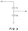
- FIG. 3 is a simplified schematic diagram of a conventional capacitive divider network.
- a typical floating gate memory device 10 programmable in accordance with this invention includes a gate 12 to which electrical potential can be applied via gate lead 14, a write or programming channel 30 connected between a programming source 32 and a programming drain 34, and a read channel 40 connected between a read source 42 and a read drain 44.
- Device 10 also includes floating gate 20 which is not an externally accessible electrode (i.e., potential cannot be directly applied to floating gate 20).
- a relatively high voltage such as 15 volts is applied to gate 12 via lead 14
- a somewhat lower voltage such as 8 volts is applied to programming drain 34
- programming source 32 is connected to ground (0 volts)
- read source 42 and drain 44 are not used and are customarily connected to ground.
- the inherent capacitive coupling between gate 12 and floating gate 20 initially raises the potential of floating gate 20 to a predetermined fraction of the gate 12 potential.
- the potential of floating gate 20 may initially be approximately 0.7 times the gate 12 potential (e.g., 10.5 volts).
- this negative charge is large enough, it makes it impossible for either 0 or 5 volts on gate 12 during normal logical operation of the device to raise the potential on floating gate 20 high enough for the floating poly transistor to turn on.
- the floating poly transistor has a threshold voltage of about 1 volt, so floating gate 20 would need to rise from -4 volts to 1 volt just to begin to allow the read channel to begin to conduct. This would require gate 12 to rise by 0 + (1 - (-4))/0.7 or 7.1 volts. Because 7.1 volts is outside of the 5 volt operating range of the circuit in end use, the transistor effectively cannot be turned on.
- read source 42 is connected to ground (0 volts)
- 5 volts is applied to read drain 44
- write channel 30 is not used (i.e., its source 32 and drain 34 are connected to ground)
- gate 12 is switched between 0 volts and 5 volts.
- a "programmed” device 10 therefore remains off at all times during normal logical operation. If device 10 is left “unprogrammed” (i.e., no charge is put on floating gate 20), then during normal logical operation, read channel 40 is off when gate 12 is at 0 volts and on (i.e., conducting) when gate 12 is at 5 volts.
- Device 10 must be at least a predetermined minimum size in order to be able to withstand the relatively high voltage (e.g., 15 volts) conventionally used during programming.
- These size limitations are both vertical dimensions (dielectric thicknesses) and planar dimensions such as channel length and spacings of electrodes.
- the dielectric thicknesses are limited by dielectric breakdown (units are volts/cm) when the voltage divided by the thickness exceeds about 107 volts/cm.
- the lateral dimensions are limited by the process technology limitations, but the larger the voltage difference between two diffusions, the larger the space required between them.
- floating gate 20 cannot be made to store sufficient charge to prevent read channel 40 from conducting when gate 12 is raised to 5 volts during normal logical operation.
- the need to program device 10 has therefore heretofore limited the device size reductions available.
- the present invention makes it possible to substantially lower the programming voltage which must be applied to gate 12 in order to raise floating gate 20 to the potential required to attract sufficient hot electrons to program the device. This is accomplished by applying a positive voltage to read source 42 and read drain 44 during programming.
- the inherent capacitive coupling between read channel 40 and floating gate 20 adds to the inherent capacitive coupling between gate 12 and floating gate 20. Accordingly, the programming potential applied to elements 42 and 44 allows the programming potential applied to gate 12 to be reduced, thereby allowing device 10 to be made smaller than would otherwise be possible.
- FIG. 2 is a table showing various illustrative values of V12 (the potential applied to gate 12), V4244 (the potential applied to read source 42 and read drain 44 in accordance with this invention), and the resulting V20 (the potential on floating gate 20) during programming, on the assumption that the inherent capacitive coupling between elements 12 and 20 is a factor of 0.7 and the inherent capacitive coupling between elements 20 and 40 is 0.3. (In all cases the conventional voltages described above are applied to write source 32 and write drain 34.) The first line in FIG. 2 shows the conventional strategy of applying 15 volts to gate 12 and not using read channel 40 during programming. The resulting initial potential on floating gate 20 is therefore 10.5 volts, which, as described above, produces satisfactory programming of device 10.
- the second line of FIG. 2 is an example of programming in accordance with this invention.
- the potential applied to gate 12 is reduced to 12.5 volts.
- the potential applied to read source 42 and read drain 44 is 5 volts.
- the third line of FIG. 2 shows another example of programming in accordance with this invention.
- 11 volts is applied to gate 12 and 8 volts is applied to read source 42 and read drain 44.
- the resulting initial potential on floating gate 20 is 10.1 volts, which will again produce satisfactory programming of device 10.
- Programming time may be reduced by a factor on the order of 5 (i.e., only one-fifth the programming time may be required) or 10 (i.e., only one-tenth the programming time may be required) in this way.
- Various combinations of reduced programming voltage and reduced programming time may also be employed.
- the fifth line of FIG. 2 shows the use of 14 volts applied to gate 12 with 5 volts applied to read source 42 and read drain 44 to produce an initial potential of 11.3 volts on floating gate 20. As compared to conventional programming (FIG. 2, line 1), this is a one-volt decrease in programming potential, combined with considerably faster programming (because V20 is initially substantially higher).
Abstract
Description
- This invention relates to floating gate memory devices, and more particularly to methods of programming such memory devices. The invention is pertinent to floating gate devices with separately optimized read and programming transistors coupled by a common floating gate, and which further are programmed by gate currents in the programming-optimized transistor. See, for example, B. Eitan et al. "Hot-Electron Injection into the Oxide in n-Channel MOS Devices", IEEE Transactions on Electron Devices, Vol. ED-28, No. 3, March 1981, pp. 328-40. The invention will be fully understood from the following explanation of it in the context of metal oxide semiconductor ("MOS") erasable programmable read-only memory ("EPROM") devices.
- A typical MOS EPROM device which is programmable in accordance with this invention has a control gate (sometimes referred to simply as the gate), a floating gate, a source and drain pair for programming the device, and a source and drain pair for reading the programmed state of the device. The unprogrammed initial voltage condition of the floating gate is for the capacitance between the floating gate and the source to be relaxed (i.e., 0 volts) when the gate voltage Vcg = 0. This initial condition is important because in a capacitive divider such as shown in FIG. 3 the potential of the floating gate Vfg is given by the equation

- The device is conventionally programmed by applying a relatively high voltage (e.g., 15 volts) to the gate and a somewhat lower voltage (e.g., 8 volts) to the programming drain, while holding the programming source at ground potential (i.e., 0 volts). Capacitive coupling between the control gate and the floating gate causes a change in the potential of the floating gate when the potential of the control gate is changed. For example, if the capacitive divide or coupling ratio is assumed to be 0.7 and both the control gate and the floating gate are initially at 0 volts, then raising the control gate to 15 volts causes the floating gate potential to rise to 10.5 volts. The programming transistor's channel begins to conduct a substantial current. Due to the very high field in the drain region, electron hole pairs are formed with a very high kinetic energy. Some of the electrons will have enough kinetic energy to be injected onto the floating gate where they are trapped. This in turn lowers the potential of the floating gate (e.g., to approximately 6.5 volts in the example being discussed), thereby "programming" the device.
- When the control gate potential is lowered from 15 volts to 0 volts, the capacitive divider causes a 10.5 volt drop in potential from 6.5 volts to -4 volts on the floating gate. Because the floating gate transistor is an NMOS transistor with a threshold voltage of about 1 volt, the floating gate transistor is non-conducting. Furthermore, when the control gate is raised to 5 volts, there results a 3.5 volt rise on the floating gate to -0.5 voltage. The programmed transistor therefore remains off. In other words, the read channel of a programmed device is always off regardless of the normal logic level (0 or 5 volts) applied to the gate of the device. In an unprogrammed device (i.e., no negative charge on the floating gate), the read channel of the device is on or off depending on whether 5 volts or 0 volts, respectively, is applied to the gate of the device because the floating gate potential is respectively 3.5 volts (above the threshold) or 0 volts (below the threshold).
- As floating gate devices are made smaller, their ability to withstand the relatively high voltages (e.g., the above-mentioned 15 volts) conventionally required to program them decreases. Accordingly, the ability to withstand these voltages has become a limitation on further device size reduction which would otherwise be possible and very advantageous.
- It is therefore, an object of this invention to reduce the voltages required to program floating gate memory devices.
- It is another object of this invention to reduce the time required to program floating gate memory devices.
- These and other objects of the invention are accomplished in accordance with the principles of the invention by using the inherent capacitive coupling between the channel of the read device and the floating gate to increase the voltage on the floating gate during programming. In the example discussed above, a positive voltage (e.g., 5-10 volts) is applied to both the read source and the read drain during programming. This raises the potential of the floating gate beyond what can be achieved solely by applying a positive voltage to the gate as is conventional. Accordingly, the gate programming potential can be lowered (e.g., from 15 volts to 12.5 or even 10 volts), or programming time can be shortened, or a combination of these two advantages can be realized.
- Further features of the invention, its nature and various advantages will be more apparent from the accompanying drawings and the following detailed description of the preferred embodiments.
- FIG. 1 is a simplified schematic diagram of an illustrative floating gate memory device which can be programmed in accordance with the method of this invention.
- FIG. 2 is a chart of various possible voltages in the floating gate memory device shown in FIG. 1 during conventional programming (first line) and during programming in accordance with this invention (subsequent lines).
- FIG. 3 is a simplified schematic diagram of a conventional capacitive divider network.
- As shown in FIG. 1 a typical floating
gate memory device 10 programmable in accordance with this invention includes agate 12 to which electrical potential can be applied viagate lead 14, a write orprogramming channel 30 connected between aprogramming source 32 and aprogramming drain 34, and a readchannel 40 connected between aread source 42 and aread drain 44.Device 10 also includesfloating gate 20 which is not an externally accessible electrode (i.e., potential cannot be directly applied to floating gate 20). - During conventional programming a relatively high voltage such as 15 volts is applied to
gate 12 vialead 14, a somewhat lower voltage such as 8 volts is applied toprogramming drain 34,programming source 32 is connected to ground (0 volts), and readsource 42 anddrain 44 are not used and are customarily connected to ground. The inherent capacitive coupling betweengate 12 and floatinggate 20 initially raises the potential of floatinggate 20 to a predetermined fraction of thegate 12 potential. For example, the potential of floatinggate 20 may initially be approximately 0.7 times thegate 12 potential (e.g., 10.5 volts). Some of the electrons flowing throughchannel 30 are consequently injected ontofloating gate 20 and remain there, thereby lowering the potential of the floating gate and leaving a negative charge on the floating gate. If, as is desired, this negative charge is large enough, it makes it impossible for either 0 or 5 volts ongate 12 during normal logical operation of the device to raise the potential on floatinggate 20 high enough for the floating poly transistor to turn on. The floating poly transistor has a threshold voltage of about 1 volt, so floatinggate 20 would need to rise from -4 volts to 1 volt just to begin to allow the read channel to begin to conduct. This would requiregate 12 to rise by 0 + (1 - (-4))/0.7 or 7.1 volts. Because 7.1 volts is outside of the 5 volt operating range of the circuit in end use, the transistor effectively cannot be turned on. During such end use or normal operation, readsource 42 is connected to ground (0 volts), 5 volts is applied to readdrain 44, writechannel 30 is not used (i.e., itssource 32 anddrain 34 are connected to ground), andgate 12 is switched between 0 volts and 5 volts. A "programmed"device 10 therefore remains off at all times during normal logical operation. Ifdevice 10 is left "unprogrammed" (i.e., no charge is put on floating gate 20), then during normal logical operation, readchannel 40 is off whengate 12 is at 0 volts and on (i.e., conducting) whengate 12 is at 5 volts. In the case of an unprogrammed device, a 5 volt rise ongate 12 results in a potential of 0 + .7(5) = 3.5 volts on the floating gate. Because this is greater than the 1 volt threshold voltage of the floating poly transistor, the transistor conducts. -
Device 10 must be at least a predetermined minimum size in order to be able to withstand the relatively high voltage (e.g., 15 volts) conventionally used during programming. These size limitations are both vertical dimensions (dielectric thicknesses) and planar dimensions such as channel length and spacings of electrodes. The dielectric thicknesses are limited by dielectric breakdown (units are volts/cm) when the voltage divided by the thickness exceeds about 10⁷ volts/cm. The lateral dimensions are limited by the process technology limitations, but the larger the voltage difference between two diffusions, the larger the space required between them. If the above-mentioned relatively high voltage is not used during conventional programming, floatinggate 20 cannot be made to store sufficient charge to prevent readchannel 40 from conducting whengate 12 is raised to 5 volts during normal logical operation. The need to programdevice 10 has therefore heretofore limited the device size reductions available. - The present invention makes it possible to substantially lower the programming voltage which must be applied to
gate 12 in order to raisefloating gate 20 to the potential required to attract sufficient hot electrons to program the device. This is accomplished by applying a positive voltage to readsource 42 and readdrain 44 during programming. The inherent capacitive coupling between readchannel 40 and floatinggate 20 adds to the inherent capacitive coupling betweengate 12 and floatinggate 20. Accordingly, the programming potential applied toelements gate 12 to be reduced, thereby allowingdevice 10 to be made smaller than would otherwise be possible. - FIG. 2 is a table showing various illustrative values of V12 (the potential applied to gate 12), V4244 (the potential applied to read
source 42 and readdrain 44 in accordance with this invention), and the resulting V20 (the potential on floating gate 20) during programming, on the assumption that the inherent capacitive coupling betweenelements elements source 32 and writedrain 34.) The first line in FIG. 2 shows the conventional strategy of applying 15 volts togate 12 and not using readchannel 40 during programming. The resulting initial potential on floatinggate 20 is therefore 10.5 volts, which, as described above, produces satisfactory programming ofdevice 10. - The second line of FIG. 2 is an example of programming in accordance with this invention. The potential applied to
gate 12 is reduced to 12.5 volts. The potential applied to readsource 42 and readdrain 44 is 5 volts. The resulting initial potential on floatinggate 20 is therefore (12.5)(0.7) + (5)(0.3) = 10.25 volts, which again produces satisfactory programming ofdevice 10. - The third line of FIG. 2 shows another example of programming in accordance with this invention. In this example, 11 volts is applied to
gate source 42 and readdrain 44. The resulting initial potential on floatinggate 20 is 10.1 volts, which will again produce satisfactory programming ofdevice 10. - It will be understood that the inherent capacitive coupling factors (assumed to be 0.7 and 0.3 above) may vary, and that this may make it possible to use different values and/or combinations of V12 and V4244 in accordance with this invention to produce satisfactory programming of
device 10. It will also be noted that the principles of this invention can alternatively or additionally be used to shorten the time required to programdevice 12. This is illustrated by the fourth line of FIG. 2 where the conventional programming voltage (15 volts) applied togate 12 is supplemented by a voltage (e.g., 5 volts) applied to readsource 42 and readdrain 44. The resulting 12 volts on floatinggate 20 causes the floating gate to charge much faster than the conventional 10.5 volts (FIG. 2, first line). Programming time may be reduced by a factor on the order of 5 (i.e., only one-fifth the programming time may be required) or 10 (i.e., only one-tenth the programming time may be required) in this way. Various combinations of reduced programming voltage and reduced programming time may also be employed. For example, the fifth line of FIG. 2 shows the use of 14 volts applied togate 12 with 5 volts applied to readsource 42 and readdrain 44 to produce an initial potential of 11.3 volts on floatinggate 20. As compared to conventional programming (FIG. 2, line 1), this is a one-volt decrease in programming potential, combined with considerably faster programming (because V20 is initially substantially higher). - It will be understood that the foregoing is merely illustrative of the principles of this invention and that various modifications can be made by those skilled in the art without departing from the scope and spirit of the invention. For example, various other capacitive coupling factors will make possible various other combinations of V12, V4244, and V20.
Claims (15)
- The method of programming a floating gate memory device having a gate terminal, a programming channel connected between a programming source terminal and a programming drain terminal, a read channel connected between a read source terminal and a read drain terminal, and a floating gate capacitively coupled to said gate terminal and to said read channel, said method comprising the at least partly concurrent steps of:
applying a first programming voltage to said gate terminal;
applying a second programming voltage to said programming source terminal;
applying a third programming voltage to said programming drain terminal;
applying a fourth programming voltage to said read source terminal; and
applying a fifth programming voltage to said read drain terminal, wherein said first, third, fourth, and fifth programming voltages have a predetermined polarity relative to said second programming voltage. - The method defined in claim 1 wherein said second programming voltage is ground potential and all of said first, third, fourth, and fifth programming voltages are positive.
- The method defined in claim 1 wherein said fourth and fifth programming voltages are substantially the same.
- The method defined in claim 2 wherein said first programming voltage is greater than said third programming voltage, and wherein said third programming voltage is greater than said fourth and fifth programming voltages.
- The method defined in claim 4 wherein said fourth and fifth programming voltages are substantially equal.
- The method defined in claim 1 wherein said device is a MOS EPROM device, wherein said first, third, fourth, and fifth programming voltages are positive, and wherein said second programming voltage is ground potential.
- The method defined in claim 6 wherein said first programming voltage is greater than said third programming voltage, and wherein said fourth and fifth programming voltages are substantially equal.
- The method defined in claim 7 wherein said fourth and fifth programming voltages are less than said third programming voltage.
- The method defined in claim 8 wherein said first programming voltage is approximately 15 volts, wherein said second programming voltage is approximately 8 volts, and wherein said fourth and fifth programming voltages are approximately 5 volts.
- The method defined in claim 8 wherein said first programming voltage is substantially less than 15 volts, wherein said third programming voltage is approximately 8 volts, and wherein said fourth and fifth programming voltages are approximately 5 volts.
- The method defined in claim 10 wherein said first programming voltage is at least one volt less than 15 volts.
- The method defined in claim 1 wherein the initial voltage of said floating gate as a result of performance of said applying steps is approximately equal to the initial voltage of said floating gate when said device is programmed in a conventional manner with the same voltage applied to the read source terminal and the read drain terminal as is applied to said programming source terminal.
- The method defined in claim 1 wherein the initial voltage of said floating gate as a result of performance of said applying steps is greater than the initial voltage of said floating gate when said device is programmed in a conventional manner with the same voltage applied to the read source terminal and the read drain terminal as is applied to said programming source terminal.
- The method of programming a MOS EPROM having a gate terminal, a programming channel connected between a programming source terminal and a programming drain terminal, a read channel connected between a read source terminal and a read drain terminal, and a floating gate capacitively coupled to said gate terminal and to said read channel, said method comprising the at least partly concurrent steps of:
applying ground potential to said programming source terminal;
applying a first positive voltage to said gate terminal;
applying a second positive voltage to said programming drain terminal; and
applying a third positive voltage to said read source terminal and said read drain terminal. - The method defined in claim 14 wherein said second positive voltage is less than said first positive voltage but more than said third positive voltage.
Applications Claiming Priority (2)
| Application Number | Priority Date | Filing Date | Title |
|---|---|---|---|
| US07/708,241 US5247477A (en) | 1991-05-31 | 1991-05-31 | Method of programming floating gate memory devices aided by potential applied to read channel |
| US708241 | 1996-09-03 |
Publications (3)
| Publication Number | Publication Date |
|---|---|
| EP0516296A2 true EP0516296A2 (en) | 1992-12-02 |
| EP0516296A3 EP0516296A3 (en) | 1993-10-06 |
| EP0516296B1 EP0516296B1 (en) | 1997-09-10 |
Family
ID=24844973
Family Applications (1)
| Application Number | Title | Priority Date | Filing Date |
|---|---|---|---|
| EP92304071A Expired - Lifetime EP0516296B1 (en) | 1991-05-31 | 1992-05-06 | Method of programming floating gate memory devices |
Country Status (4)
| Country | Link |
|---|---|
| US (1) | US5247477A (en) |
| EP (1) | EP0516296B1 (en) |
| JP (1) | JPH0652692A (en) |
| DE (1) | DE69222087D1 (en) |
Families Citing this family (6)
| Publication number | Priority date | Publication date | Assignee | Title |
|---|---|---|---|---|
| JP2829156B2 (en) * | 1991-07-25 | 1998-11-25 | 株式会社東芝 | Redundancy circuit for nonvolatile semiconductor memory device |
| US5349220A (en) * | 1993-08-10 | 1994-09-20 | United Microelectronics Corporation | Flash memory cell and its operation |
| US5909049A (en) | 1997-02-11 | 1999-06-01 | Actel Corporation | Antifuse programmed PROM cell |
| US6125059A (en) * | 1999-05-14 | 2000-09-26 | Gatefield Corporation | Method for erasing nonvolatile memory cells in a field programmable gate array |
| JP2008257804A (en) * | 2007-04-05 | 2008-10-23 | Renesas Technology Corp | Semiconductor device |
| US8384147B2 (en) * | 2011-04-29 | 2013-02-26 | Silicon Storage Technology, Inc. | High endurance non-volatile memory cell and array |
Citations (2)
| Publication number | Priority date | Publication date | Assignee | Title |
|---|---|---|---|---|
| US4663740A (en) * | 1985-07-01 | 1987-05-05 | Silicon Macrosystems Incorporated | High speed eprom cell and array |
| US4982377A (en) * | 1988-12-27 | 1991-01-01 | Nec Corporation | Erasable programmable read only memory device improved in operation speed and in the amount of read out current |
Family Cites Families (5)
| Publication number | Priority date | Publication date | Assignee | Title |
|---|---|---|---|---|
| US4412310A (en) * | 1980-10-14 | 1983-10-25 | Intel Corporation | EPROM Cell with reduced programming voltage and method of fabrication |
| FR2622038B1 (en) * | 1987-10-19 | 1990-01-19 | Thomson Semiconducteurs | METHOD FOR PROGRAMMING MEMORY CELLS OF A MEMORY AND CIRCUIT FOR IMPLEMENTING SAID METHOD |
| US5122985A (en) * | 1990-04-16 | 1992-06-16 | Giovani Santin | Circuit and method for erasing eeprom memory arrays to prevent over-erased cells |
| US5132935A (en) * | 1990-04-16 | 1992-07-21 | Ashmore Jr Benjamin H | Erasure of eeprom memory arrays to prevent over-erased cells |
| US5150179A (en) * | 1990-07-05 | 1992-09-22 | Texas Instruments Incorporated | Diffusionless source/drain conductor electrically-erasable, electrically-programmable read-only memory and method for making and using the same |
-
1991
- 1991-05-31 US US07/708,241 patent/US5247477A/en not_active Expired - Lifetime
-
1992
- 1992-05-06 DE DE69222087T patent/DE69222087D1/en not_active Expired - Lifetime
- 1992-05-06 EP EP92304071A patent/EP0516296B1/en not_active Expired - Lifetime
- 1992-05-28 JP JP13678792A patent/JPH0652692A/en active Pending
Patent Citations (2)
| Publication number | Priority date | Publication date | Assignee | Title |
|---|---|---|---|---|
| US4663740A (en) * | 1985-07-01 | 1987-05-05 | Silicon Macrosystems Incorporated | High speed eprom cell and array |
| US4982377A (en) * | 1988-12-27 | 1991-01-01 | Nec Corporation | Erasable programmable read only memory device improved in operation speed and in the amount of read out current |
Also Published As
| Publication number | Publication date |
|---|---|
| EP0516296A3 (en) | 1993-10-06 |
| US5247477A (en) | 1993-09-21 |
| DE69222087D1 (en) | 1997-10-16 |
| EP0516296B1 (en) | 1997-09-10 |
| JPH0652692A (en) | 1994-02-25 |
Similar Documents
| Publication | Publication Date | Title |
|---|---|---|
| US4096402A (en) | MOSFET buffer for TTL logic input and method of operation | |
| US6853583B2 (en) | Method and apparatus for preventing overtunneling in pFET-based nonvolatile memory cells | |
| US5677873A (en) | Methods of programming flash EEPROM integrated circuit memory devices to prevent inadvertent programming of nondesignated NAND memory cells therein | |
| US7573749B2 (en) | Counteracting overtunneling in nonvolatile memory cells | |
| EP0586473B1 (en) | Non-volatile erasable and programmable interconnect cell | |
| KR20030014212A (en) | Electrically-eraseable programmable read-only memory having reduced-page-size program and erase | |
| EP1575057A2 (en) | Floating gate nonvolatile memory circuits and methods | |
| US20070058434A1 (en) | Nonvolatile memory cell programming | |
| EP0866466A2 (en) | Biasing scheme for reducing stress and improving reliability in EEPROM cells | |
| DE102007007585B4 (en) | Circuit arrangement and method for operating a circuit arrangement | |
| US5220528A (en) | Compensation circuit for leakage in flash EPROM | |
| US5247477A (en) | Method of programming floating gate memory devices aided by potential applied to read channel | |
| US10446235B2 (en) | Method for writing in an EEPROM memory and corresponding device | |
| US4348745A (en) | Non-volatile random access memory having non-inverted storage | |
| US20030012054A1 (en) | Methods of operating semiconductor memory devices having split gate-type non-volatile memory cells | |
| US7236398B1 (en) | Structure of a split-gate memory cell | |
| US5736891A (en) | Discharge circuit in a semiconductor memory | |
| US6459616B1 (en) | Split common source on EEPROM array | |
| Millard et al. | Calibration and matching of floating gate devices | |
| US6549016B1 (en) | Negative voltage detector | |
| EP0430455A2 (en) | Nonvolatile memory device and operating method | |
| US6195295B1 (en) | Segmented column memory device voltage steering technique | |
| JPH1116383A (en) | Electrically writable/erasable nonvolatile semiconductor memory device | |
| KR20010065270A (en) | Method of programming a flash memory cell | |
| DE19742176C1 (en) | Procedure for use when using EEPROMs as program memory |
Legal Events
| Date | Code | Title | Description |
|---|---|---|---|
| PUAI | Public reference made under article 153(3) epc to a published international application that has entered the european phase |
Free format text: ORIGINAL CODE: 0009012 |
|
| AK | Designated contracting states |
Kind code of ref document: A2 Designated state(s): BE DE DK ES FR GB GR IT LU NL PT |
|
| PUAL | Search report despatched |
Free format text: ORIGINAL CODE: 0009013 |
|
| AK | Designated contracting states |
Kind code of ref document: A3 Designated state(s): BE DE DK ES FR GB GR IT LU NL PT |
|
| 17P | Request for examination filed |
Effective date: 19940221 |
|
| GRAG | Despatch of communication of intention to grant |
Free format text: ORIGINAL CODE: EPIDOS AGRA |
|
| 17Q | First examination report despatched |
Effective date: 19960909 |
|
| GRAH | Despatch of communication of intention to grant a patent |
Free format text: ORIGINAL CODE: EPIDOS IGRA |
|
| GRAH | Despatch of communication of intention to grant a patent |
Free format text: ORIGINAL CODE: EPIDOS IGRA |
|
| GRAA | (expected) grant |
Free format text: ORIGINAL CODE: 0009210 |
|
| AK | Designated contracting states |
Kind code of ref document: B1 Designated state(s): BE DE DK ES FR GB GR IT LU NL PT |
|
| PG25 | Lapsed in a contracting state [announced via postgrant information from national office to epo] |
Ref country code: IT Free format text: LAPSE BECAUSE OF FAILURE TO SUBMIT A TRANSLATION OF THE DESCRIPTION OR TO PAY THE FEE WITHIN THE PRE;WARNING: LAPSES OF ITALIAN PATENTS WITH EFFECTIVE DATE BEFORE 2007 MAY HAVE OCCURRED AT ANY TIME BEFORE 2007. THE CORRECT EFFECTIVE DATE MAY BE DIFFERENT FROM THE ONE RECORDED.SCRIBED TIME-LIMIT Effective date: 19970910 Ref country code: FR Free format text: LAPSE BECAUSE OF FAILURE TO SUBMIT A TRANSLATION OF THE DESCRIPTION OR TO PAY THE FEE WITHIN THE PRESCRIBED TIME-LIMIT Effective date: 19970910 Ref country code: ES Free format text: THE PATENT HAS BEEN ANNULLED BY A DECISION OF A NATIONAL AUTHORITY Effective date: 19970910 Ref country code: BE Effective date: 19970910 Ref country code: GR Free format text: LAPSE BECAUSE OF FAILURE TO SUBMIT A TRANSLATION OF THE DESCRIPTION OR TO PAY THE FEE WITHIN THE PRESCRIBED TIME-LIMIT Effective date: 19970910 Ref country code: NL Free format text: LAPSE BECAUSE OF FAILURE TO SUBMIT A TRANSLATION OF THE DESCRIPTION OR TO PAY THE FEE WITHIN THE PRESCRIBED TIME-LIMIT Effective date: 19970910 Ref country code: DK Free format text: LAPSE BECAUSE OF NON-PAYMENT OF DUE FEES Effective date: 19970910 |
|
| REF | Corresponds to: |
Ref document number: 69222087 Country of ref document: DE Date of ref document: 19971016 |
|
| PG25 | Lapsed in a contracting state [announced via postgrant information from national office to epo] |
Ref country code: PT Effective date: 19971210 |
|
| PG25 | Lapsed in a contracting state [announced via postgrant information from national office to epo] |
Ref country code: DE Free format text: LAPSE BECAUSE OF FAILURE TO SUBMIT A TRANSLATION OF THE DESCRIPTION OR TO PAY THE FEE WITHIN THE PRESCRIBED TIME-LIMIT Effective date: 19971211 |
|
| REG | Reference to a national code |
Ref country code: GB Ref legal event code: 732E |
|
| EN | Fr: translation not filed | ||
| NLV1 | Nl: lapsed or annulled due to failure to fulfill the requirements of art. 29p and 29m of the patents act | ||
| PG25 | Lapsed in a contracting state [announced via postgrant information from national office to epo] |
Ref country code: LU Free format text: LAPSE BECAUSE OF NON-PAYMENT OF DUE FEES Effective date: 19980506 |
|
| PLBE | No opposition filed within time limit |
Free format text: ORIGINAL CODE: 0009261 |
|
| STAA | Information on the status of an ep patent application or granted ep patent |
Free format text: STATUS: NO OPPOSITION FILED WITHIN TIME LIMIT |
|
| 26N | No opposition filed | ||
| REG | Reference to a national code |
Ref country code: GB Ref legal event code: IF02 |
|
| PGFP | Annual fee paid to national office [announced via postgrant information from national office to epo] |
Ref country code: GB Payment date: 20050406 Year of fee payment: 14 |
|
| PG25 | Lapsed in a contracting state [announced via postgrant information from national office to epo] |
Ref country code: GB Free format text: LAPSE BECAUSE OF NON-PAYMENT OF DUE FEES Effective date: 20060506 |
|
| GBPC | Gb: european patent ceased through non-payment of renewal fee |
Effective date: 20060506 |