EP0514976A2 - Combined read/write magnetic head - Google Patents
Combined read/write magnetic head Download PDFInfo
- Publication number
- EP0514976A2 EP0514976A2 EP92201355A EP92201355A EP0514976A2 EP 0514976 A2 EP0514976 A2 EP 0514976A2 EP 92201355 A EP92201355 A EP 92201355A EP 92201355 A EP92201355 A EP 92201355A EP 0514976 A2 EP0514976 A2 EP 0514976A2
- Authority
- EP
- European Patent Office
- Prior art keywords
- mre
- head
- magnetic head
- read
- write
- Prior art date
- Legal status (The legal status is an assumption and is not a legal conclusion. Google has not performed a legal analysis and makes no representation as to the accuracy of the status listed.)
- Granted
Links
Images
Classifications
-
- G—PHYSICS
- G11—INFORMATION STORAGE
- G11B—INFORMATION STORAGE BASED ON RELATIVE MOVEMENT BETWEEN RECORD CARRIER AND TRANSDUCER
- G11B5/00—Recording by magnetisation or demagnetisation of a record carrier; Reproducing by magnetic means; Record carriers therefor
- G11B5/127—Structure or manufacture of heads, e.g. inductive
- G11B5/31—Structure or manufacture of heads, e.g. inductive using thin films
-
- G—PHYSICS
- G11—INFORMATION STORAGE
- G11B—INFORMATION STORAGE BASED ON RELATIVE MOVEMENT BETWEEN RECORD CARRIER AND TRANSDUCER
- G11B5/00—Recording by magnetisation or demagnetisation of a record carrier; Reproducing by magnetic means; Record carriers therefor
- G11B5/127—Structure or manufacture of heads, e.g. inductive
- G11B5/33—Structure or manufacture of flux-sensitive heads, i.e. for reproduction only; Combination of such heads with means for recording or erasing only
- G11B5/39—Structure or manufacture of flux-sensitive heads, i.e. for reproduction only; Combination of such heads with means for recording or erasing only using magneto-resistive devices or effects
- G11B5/3903—Structure or manufacture of flux-sensitive heads, i.e. for reproduction only; Combination of such heads with means for recording or erasing only using magneto-resistive devices or effects using magnetic thin film layers or their effects, the films being part of integrated structures
- G11B5/3906—Details related to the use of magnetic thin film layers or to their effects
- G11B5/3916—Arrangements in which the active read-out elements are coupled to the magnetic flux of the track by at least one magnetic thin film flux guide
- G11B5/3919—Arrangements in which the active read-out elements are coupled to the magnetic flux of the track by at least one magnetic thin film flux guide the guide being interposed in the flux path
- G11B5/3922—Arrangements in which the active read-out elements are coupled to the magnetic flux of the track by at least one magnetic thin film flux guide the guide being interposed in the flux path the read-out elements being disposed in magnetic shunt relative to at least two parts of the flux guide structure
- G11B5/3925—Arrangements in which the active read-out elements are coupled to the magnetic flux of the track by at least one magnetic thin film flux guide the guide being interposed in the flux path the read-out elements being disposed in magnetic shunt relative to at least two parts of the flux guide structure the two parts being thin films
-
- G—PHYSICS
- G11—INFORMATION STORAGE
- G11B—INFORMATION STORAGE BASED ON RELATIVE MOVEMENT BETWEEN RECORD CARRIER AND TRANSDUCER
- G11B5/00—Recording by magnetisation or demagnetisation of a record carrier; Reproducing by magnetic means; Record carriers therefor
- G11B5/127—Structure or manufacture of heads, e.g. inductive
- G11B5/31—Structure or manufacture of heads, e.g. inductive using thin films
- G11B5/3103—Structure or manufacture of integrated heads or heads mechanically assembled and electrically connected to a support or housing
-
- G—PHYSICS
- G11—INFORMATION STORAGE
- G11B—INFORMATION STORAGE BASED ON RELATIVE MOVEMENT BETWEEN RECORD CARRIER AND TRANSDUCER
- G11B5/00—Recording by magnetisation or demagnetisation of a record carrier; Reproducing by magnetic means; Record carriers therefor
- G11B5/127—Structure or manufacture of heads, e.g. inductive
- G11B5/31—Structure or manufacture of heads, e.g. inductive using thin films
- G11B5/3109—Details
- G11B5/3113—Details for improving the magnetic domain structure or avoiding the formation or displacement of undesirable magnetic domains
-
- G—PHYSICS
- G11—INFORMATION STORAGE
- G11B—INFORMATION STORAGE BASED ON RELATIVE MOVEMENT BETWEEN RECORD CARRIER AND TRANSDUCER
- G11B5/00—Recording by magnetisation or demagnetisation of a record carrier; Reproducing by magnetic means; Record carriers therefor
- G11B5/127—Structure or manufacture of heads, e.g. inductive
- G11B5/33—Structure or manufacture of flux-sensitive heads, i.e. for reproduction only; Combination of such heads with means for recording or erasing only
- G11B5/39—Structure or manufacture of flux-sensitive heads, i.e. for reproduction only; Combination of such heads with means for recording or erasing only using magneto-resistive devices or effects
- G11B5/3903—Structure or manufacture of flux-sensitive heads, i.e. for reproduction only; Combination of such heads with means for recording or erasing only using magneto-resistive devices or effects using magnetic thin film layers or their effects, the films being part of integrated structures
- G11B5/3967—Composite structural arrangements of transducers, e.g. inductive write and magnetoresistive read
Definitions
- the invention pertains generally to magnetic heads, and more particularly to combined read/write magnetic heads.
- a write magnetic head is a device used to magnetize regions of a magnetic medium, e.g., a magnetic tape, and thereby "write” information onto the magnetic medium.
- a read magnetic head is a device used to detect magnetized regions on a magnetic medium, and thereby "read” information on the magnetic medium.
- a write magnetic head includes a magnetic yoke having a gap exhibiting a relatively high magnetic reluctance, e.g., an air gap.
- An electric coil encircles the yoke. By passing an electric current through the coil, a magnetic field is produced extending through the yoke.
- the corresponding fringing magnetic field at the gap is used to magnetize regions of, and thereby write information onto, a magnetic medium, e.g., a magnetic tape, positioned adjacent to, and moving past, the gap.
- a conventional read magnetic head is generally similar to the write magnetic head described above.
- a magnetic medium e.g., a magnetic tape
- Magnetic flux emanating from magnetized regions in the magnetic medium, is coupled into the yoke via the gap.
- Time-wise variations in magnetic flux induce an output voltage across the coil encircling the magnetic yoke.
- Read magnetic heads have been developed in which the output voltage is proportional to magnetic flux, rather than time-wise changes in magnetic flux.
- a read head typically employs a magnetoresistive element (MRE).
- MRE magnetoresistive element
- the electrical resistance of the MRE, and therefore the voltage drop across the MRE is related to the angle between the direction of magnetization and the direction of current flow. If the MRE is exposed to an external magnetic field, e.g., a magnetic field emanating from a magnetic tape, which external field is, for example, oriented transversely to the initial magnetization direction of the MRE, then the magnetization direction will necessarily be changed and the MRE will exhibit a corresponding change in resistance.
- the change in resistance of an MRE is a nonlinear function of the field strength of the external magnetic field to be sensed.
- the MRE is preferably operated so that the angle between the initial magnetization direction and the direction of current flow is 45 degrees. This is accomplished, for example, by magnetizing the MRE along a direction which is at 45 degrees to a longitudinal direction of the MRE and flowing current along the longitudinal direction.
- the MRE is provided with a barber pole configuration of electrical conductors, i.e., spaced, parallel conductive strips applied to the surface of the MRE.
- conductive strips which constitute equipotential surfaces, are oriented so that electrical current in the MRE flows between the conductive strips at an angle of 45 degrees relative to the longitudinal direction of the MRE, along which the MRE is magnetized. (Regarding barber pole MREs, see U.S. Patent No. 4,052,748; herewith incorporated by reference).
- a read head be integrally combined with a write head in a unitary structure.
- This combined read/write head fabricated using thin-film processing, is described in "An Integrated Magnetoresistive Read, Inductive Write High Density Recording Head", C.H. Bajorek et al, Published Proceedings of 20th Annual Conference on Magnetism and Magnetic Materials, American Institute of Physics, New York, 1975, pp. 548-549 (herewith incorporated by reference).
- the known combined read/write head is formed on a non-magnetic substrate and includes a read head consisting of magnetically permeable, permalloy layers separated by a layer of substantially magnetically impermeable silicon dioxide, which defines the read gap of the read head.
- a read head consisting of magnetically permeable, permalloy layers separated by a layer of substantially magnetically impermeable silicon dioxide, which defines the read gap of the read head.
- An MRE film and an overlying permanent magnet film are buried in the silicon dioxide layer.
- the permanent magnet film serves to magnetize the MRE film in a direction which is at 45 degrees to the direction of current flow in the MRE film.
- the known read/write head also includes a write head consisting of the permalloy layer, shared with the read head, an overlying hard gold layer, which defines the write gap, and another, overlying permalloy layer.
- the permalloy layers serve as the poles of the write head.
- a layer of soft gold, buried in the hard gold layer, constitutes a one-turn write coil.
- the permalloy layers serve to shield the MRE film from the flux produced by the write head, and from other stray flux.
- flux emanating from the magnetic medium is not communicated to the MRE film by the permalloy layers because, as before, these layers serve to shield the MRE film from the flux. Rather, the only flux which reaches the MRE film is that emanating from the magnetic medium which directly impinges upon the MRE film.
- the known combined read/write head has advantageous features, it has at least one significant disadvantageous feature. That is, when a magnetic tape is drawn past the read gap, the material of the read gap undergoes wear. Because the MRE film is located in the read gap, it too undergoes wear and a corresponding degradation in sensitivity. This wear of the MRE film generally precludes commercial viability.
- JP-A 63-37811 A thin-film read head which avoids wear of the MRE is disclosed in JP-A 63-37811 (herewith incorporated by reference).
- a read head is formed on a non-magnetic substrate and includes a layer (having an undisclosed composition and function) overlying the substrate.
- An MRE overlies the layer, while an electrically insulating layer overlies the MRE. It is assumed that the MRE is a single-domain magnetic element (rather than a multi-domain element) and is thus relatively sensitive to the magnetic fields to be sensed.
- To known read head also includes a broken (discontinuous) flux guide having sections, each of which overlies the insulating layer and partially overlaps the MRE.
- An electrically insulating layer overlies the broken flux guide and defines the read gap of the read head.
- An electrical conductor, buried within the insulating layer, serves to produce a biasing magnetic field for the MRE.
- a continuous flux guide overlies the insulating layer.
- the flux guides serve to communicate flux emanating from a magnetic medium, e.g., a magnetic tape, to the MRE. That is, flux enters the continuous flux guide, is communicated to flux guide section, which communicates it to MRE, which in turn communicates it to flux guide section.
- a magnetic medium e.g., a magnetic tape
- the MRE of the known read head is located outside the read gap, and is therefore not subject to MRE wear and degradation. Therefore, in light of the teachings of said article "An Integrated Magnetoresistive Read, Inductive Write High Density Recording Head", it would appear that a commercially viable read/write head, in which the MRE does not undergo wear, is readily achieved by combining a write head with the read head known from JP-A 63-37811, with the continuous flux guide being common to both the read head and the write head. However, when this is done, new, previously unrecognized, significant problems arise, as discussed below.
- the invention involves a combined read/write head in which the read head is similar to the read head known from JP-A 63-37811 and the write head overlies the read head.
- the top flux guide of the read head is shared with, and serves as the bottom pole of, the write head.
- the invention involves the finding that when a write head is combined with the Yoda read head, the resulting magnetic circuit is such that, in general, a significant amount of the flux generated by the write head during writing is communicated to the MRE via the flux guide and flux guide sections.
- the MRE is destabilized, i.e., converted from a single-domain element to a multi-domain element, which results in substantially reduced MRE sensitivity.
- the MRE stability standards it has been found that such destabilization is avoided provided the amount of flux communicated to the MRE results in a corresponding flux density equal to or less than about 10,000 gauss, and preferably equal to or less than about 6,000 gauss, a standard hereinafter referred to as the MRE stability standards.
- the invention also involves the finding that the above magnetic circuit also leads to the write head (unintentionally) functioning as a read head. That is, during reading, flux from a portion of, for example, a magnetic tape positioned adjacent the write head is communicated via the flux guide and flux guide sections to the MRE. As a consequence, the MRE generates spurious signals, which substantially degrades signal-to-noise ratio.
- the amount of flux communicated via the write head (acting as a read head) to the MRE results in about 10 percent or less, and preferably about 5 percent or less, of the signal output of the MRE, then the corresponding signal and signal-to-noise ratio is commercially acceptable, a standard hereinafter referred to as the signal standard.
- the invention still further involves the finding that the above-described problems are avoided, i.e., the MRE stability standard and the signal standard are simultaneously achieved, while also achieving a relatively sensitive read head, by a subtle choice of thickness dimensions for the various layers constituting the combined read/write head, as well as a subtle choice for the amount of overlap between each of the broken flux guide sections of the read head and the MRE.
- the present invention largely precludes flux generated by, or entering, the writing head from being communicated via the shared flux guide to the MRE.
- this same choice of thickness dimensions and of overlap between each of the broken flux guide sections of the read head and the MRE permits flux which is to be sensed to be efficiently communicated to the MRE during reading via the shared flux guide, and permits the read head to exhibit relatively high sensitivity.
- a preferred embodiment of the inventive read/write head 210 of the present invention includes a substrate 220 of substantially magnetically impermeable material, such as the material sold under the tradename Alsimag by 3M of Minneapolis. (For purposes of the present invention, a material is substantially magnetically impermeable if its permeability is less than about 2.)
- the composition of Alsimag includes TiC as well as Al2O3, SiO2 and MgO.
- an Alsimag substrate When purchased, the surface of an Alsimag substrate is usually nonplanar, i.e., the surface typically includes 5 micrometer ( ⁇ m) -deep concavities, called “pullouts".
- a relatively thick layer 230 of electrically insulating and substantially magnetically impermeable material such as a layer of Al2O3, is deposited, e.g., sputter deposited, onto the Alsimag substrate.
- a material is electrically insulating, for purposes of the present invention, if its resistivity is greater than about 106 ⁇ -cm.
- the initial thickness of the layer 230 is 14-20 ⁇ ms.
- the surface of the layer 230 is polished to achieve a relatively smooth surface on which to deposit the MRE.
- the resulting thickness of the layer 230 is 8-15 ⁇ ms.
- conventional polishing techniques usually leave 0.5 ⁇ m - deep, sharp-cornered scratches (indentations) in the surface of the layer 230, which are undesirable because the sharp corners serve as pinning sites for magnetic domain walls, resulting in a multi-domain MRE.
- a 1 ⁇ m-thick layer 240 of electrically insulating and substantially magnetically impermeable material e.g., a 1 ⁇ m thick layer of Al2O3, is deposited onto the layer 230.
- the read head of the present invention includes a substantially single-domain MRE 250 of magnetically permeable material, such as permalloy, directly overlying the layer 240.
- a magnetically permeable material for purposes of the present invention, is one having a permeability equal to or greater than about 100.
- a substantially single-domain MRE for purposes of the present invention, is one which has no domains in the active area.
- a destabilized or multi-domain MRE for purposes of the present invention, is one which has domains in the active area.
- the MRE 250 is of permalloy
- the composition of the permalloy is, for example, 18-22 percent Fe and 82-78 percent Ni.
- the MRE 250 is readily deposited, in the form of a substantially single-domain element, onto the layer 240 using conventional techniques, such as the sputter deposition technique.
- the thickness of the MRE 250 is between about 0.025 and 0.080 ⁇ ms, preferably 0.030 to 0.035 ⁇ ms.
- the length of the MRE 250 i.e., the dimension parallel to the plane of Fig. 1 and transverse to the MRE thickness direction, is, for example, about 120-200 ⁇ ms, preferably about 160 ⁇ ms.
- the width of the MRE is typically abut 5-25 ⁇ ms.
- the MRE 250 is preferably provided with a barber pole configuration of conductive strips 260, one of which is shown in Fig. 1.
- the conductive strips include, for example, successive layers of Mo, Au and Mo, having thicknesses of, respectively, 0.03 ⁇ m, 0.23 ⁇ m and 0.09 ⁇ m.
- the width of each conductive strip is in the range of about 2-6 ⁇ ms, the spacing between successive strips is about 5-15 ⁇ ms and the angle between each conductive strip and a longitudinal direction of the MRE, along which the MRE is magnetized, is 40°-50°.
- the barber pole configuration is achieved by first depositing continuous layers of Mo, Au and Mo, using conventional deposition techniques, e.g., conventional sputter deposition techniques, and then patterning the layers into a barber pole pattern using conventional etching techniques.
- the barber pole produces a longitudinal aligning field coinciding with the easy axis of magnetization of the MRE, thus insuring stability of the MRE during normal operation of the combined read/write head.
- Electrical insulation for the conductive strips 260 is provided by depositing a layer 270 of electrically insulating and substantially magnetically impermeable material, e.g., a layer of Al2O3, onto the conductive strips using conventional deposition techniques.
- the thickness of the layer 270 is about 0.3-0.6, preferably 0.35 ⁇ ms.
- the read head of the present invention also includes a broken (discontinuous) flux guide, including flux guide sections 280a and 280b, overlying the electrically insulating layer 270.
- the flux guide sections are of magnetically permeable material such as permalloy, the composition being, for example, 19.2 percent Fe and 80.8 percent Ni.
- the flux guide sections 280a and 280b are formed, for example, by initially depositing a continuous flux guide layer and then etching away a central strip of deposited material, or by using conventional selective deposition techniques.
- the thickness of each flux guide section is about 0.2-3.0 ⁇ ms, preferably about 0.4 ⁇ m.
- the width of each flux guide section is typically about 60-180 ⁇ ms.
- each of the flux guide sections 280a and 280b partially overlaps the MRE 250 in order to couple flux into the MRE.
- the amount of overlap between each flux guide section and the MRE is preferably equal to about 2.0-8.0 ⁇ ms, preferably about 2.5 ⁇ m.
- the read head of the present invention also includes a read gap defined by a layer 290 of substantially magnetically impermeable material, e.g., a layer of Al2O3, deposited onto the broken flux guide using conventional techniques.
- the thickness of the layer 290 is about 0.2-0.9 ⁇ ms, preferably about 0.3-0.4 ⁇ ms.
- the read head of the present invention includes a test/biasing electrical conductor 300 overlying the read gap layer 290.
- An electrical conductor for purposes of the present invention, is a structure which includes material having an electrical resistivity equal to or less than about 100 ⁇ -cm.
- This conductor 300 is useful, for example, in generating magnetic fields for testing the MRE 250, and for generating a magnetic field for biasing the MRE 250, so as to linearize the signal output from the MRE. In either event, the magnetic field or fields generated by the conductor 300 are communicated to the MRE 250 via the continuous flux guide (discussed below) and broken flux guide of the read head.
- the test/biasing conductor 300 includes, for example, successive layers of Mo, Au and Mo, having thicknesses of, respectively, 0.03 ⁇ m, 0.23 ⁇ m and 0.09 ⁇ m.
- the width of the test/biasing conductor is typically between about 10 ⁇ ms and 50 ⁇ ms.
- test/biasing conductor 300 Electrical insulation for the test/biasing conductor 300 is provided by depositing a layer 310 of electrically insulating and substantially magnetically impermeable material, e.g., a layer of Al2O3, onto the test/biasing conductor.
- the thickness of the layer 310 is about 0.3-0.9 ⁇ ms, preferably about 0.4 ⁇ ms.
- the read head of the present invention further includes a continuous flux guide 320, which overlies the electrically insulating layer 310.
- the flux guide 320 is shared by, and serves as the bottom pole of, the write head of the present invention.
- the continuous flux guide 320 is of magnetically permeable material, such as permalloy, having a composition of, for example, 19.2 percent Fe and 80.8 percent Ni.
- the continuous flux guide 320 is readily deposited using conventional techniques, e.g., plating.
- the thickness of the continuous flux guide is about 2.0-4.0 ⁇ ms, preferably about 3.0 ⁇ ms.
- the width of the continuous flux guide is typically about 160-600 ⁇ ms, preferably about 180 ⁇ ms.
- the continuous flux guide 320 extends either into direct physical contact with, or into close proximity to, flux guide section 280b so as to provide a low reluctance path between the two flux guides.
- the write head of the combined read/write head 210 of the present invention includes an overlying layer 330 of substantially magnetically impermeable material, e.g., a layer of Al2O3, which defines the write gap of the present invention.
- the layer 330 has a thickness of about 0.4-1.6 ⁇ m, preferably about 0.5-0.7 ⁇ m, and is readily deposited using conventional techniques.
- the upper surface of the write gap layer 330 is nonplanar, which is a consequence of the nonplanarity introduced by the broken flux guide of the read head. While it is possible to deposit a conductor, to serve as a one-turn write coil, directly onto the write gap layer, the resulting nonuniformity in the height position of the conductor would generally preclude the possibility of using the same conductor (as a one-turn write coil) in conjunction with a plurality of adjacent write heads. In addition, if the conductor is deposited directly onto the nonplanar, upper surface of the write gap layer using, for example, conventional electroplating techniques, then the composition of the deposited conductor will generally be non-uniform, which is undesirable.
- a planarization layer 340 of substantially magnetically impermeable, electrically insulating material is first deposited onto the write gap layer 330.
- One such useful planarization layer is of photoresist material, such as the photoresist material sold under the tradename AZ4340 by AZ HOECHST of Sommerville, New Jersey.
- the photoresist layer is readily deposited using conventional spin-deposition techniques and has a thickness of about 2-4 ⁇ ms.
- An electrical conductor 350 which serves as a one-turn write coil, is readily formed on the planarization layer 340 by depositing a layer of electrically conductive material, e.g., a layer of Cu or Au, onto the planarization layer 340.
- the conductor 350 is readily deposited using conventional electroplating techniques and has a thickness of about 2-4 ⁇ ms.
- a layer 360 of electrically insulating, substantially magnetically impermeable material is deposited onto the one-turn write coil.
- the layer 360 is, for example, of photoresist material, as discussed above.
- the thickness of the layer 360 is about 2-4 ⁇ ms.
- the write head of the present invention further includes a write top pole 370 directly overlying the layer 360.
- the top pole 370 is of magnetically permeable material, such as permalloy, the composition being, for example, 19.2 percent Fe and 80.8 percent Ni.
- the thickness of the top pole 370 is about 2.0 - 4.0 ⁇ ms, preferably about 3.0 ⁇ ms and its width is typically about 160-600 ⁇ ms.
- the right side (as viewed in Fig. 1) of the top pole 370 extends either into direct physical contact with, or into close proximity to, the bottom pole 320 so as to provide a low reluctance path between the poles.
- the preferred embodiment of the read/write head having the dimensions given above, readily achieves the MRE stability standard described above, i.e., during writing, the flux density at the MRE 250 is less than about 10,000 gauss, and even less than about 6,000 gauss, and thus MRE destabilization is avoided.
- the preferred embodiment readily achieves the signal standard described above, i.e., less than about 10 percent, and even less than about 5 percent, of the signal output of the MRE 250 is due to the flux communicated by the write head (acting as a read head) to the MRE.
- the combination of dimensions, given above, is definitely subtle and that even small deviations can be significant.
- the thickness of the write gap layer 330 were increased by 1.0 ⁇ m, then, when writing with the write head, the flux density at the MRE 250 would be increased by approximately 3040 gauss, which is obviously undesirable.
- the thickness of the (shared) continuous flux guide 320 were to be increased by 1.0 ⁇ m, then, during writing, the flux density at the MRE 250 would be decreased.
- the overlap between each of the flux guide sections 280a, 280b and the MRE 250 were increased by 1.0 ⁇ m, then, during writing, the flux density at the MRE 250 would be increased by about 522 gauss.
- the thicknesses of the broken flux guide sections 280a, 280b were increased by 1.0 ⁇ m, then, during writing, the flux density at the MRE 250 would be increased by about 320 gauss.
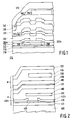
- the invention has been described in terms of a combined read/write head having a shared (common) flux guide. Other embodiments are also possible. For example, a four pole read/write head, such as that shown diagrammatically in Fig. 2, is contemplated.
- Substrate 400 supports smooth-surfaced planar layer 410, both layers of substantially magnetically impermeable material, and layer 410 also being electrically insulating.
- Layer 410 supports MRE 420, which partially underlies broken flux guide sections 440a and 440b, and is insulated electrically therefrom by layer 430.
- Test/bias conductor 460 is buried in read-gap layer 450.
- Flux guide 470 completes the read head portion R of the combined read/write head.
- the write head portion W includes bottom and top write poles 480 and 520, and write coil 510, buried in write-gap defining layer 500.
- the layer thicknesses and MRE overlap with the broken flux guide sections fall within the ranges specified for corresponding layers of Fig. 1.
- the upper flux guide 470 of the read head and bottom pole 490 of the write head each have the same thickness dimensions as the shared flux guide of Fig. 1.
- the read and write heads are separated by a substantially magnetically impermeable, electrically insulating layer 480, such as Al2O3, having a thickness typically in the range of about 2-8 ⁇ ms.
- the MRE stability standard and signal standard of the invention are achieved.
- it has the advantage of considerably less sensitivity of the MRE flux density to changes in layer thicknesses and MRE overlap than the shared flux guide embodiment of Fig. 1.
Landscapes
- Engineering & Computer Science (AREA)
- Manufacturing & Machinery (AREA)
- Magnetic Heads (AREA)
Abstract
Description
- The invention pertains generally to magnetic heads, and more particularly to combined read/write magnetic heads.
- A write magnetic head is a device used to magnetize regions of a magnetic medium, e.g., a magnetic tape, and thereby "write" information onto the magnetic medium. A read magnetic head is a device used to detect magnetized regions on a magnetic medium, and thereby "read" information on the magnetic medium.
- Conventionally, a write magnetic head includes a magnetic yoke having a gap exhibiting a relatively high magnetic reluctance, e.g., an air gap. An electric coil encircles the yoke. By passing an electric current through the coil, a magnetic field is produced extending through the yoke. The corresponding fringing magnetic field at the gap is used to magnetize regions of, and thereby write information onto, a magnetic medium, e.g., a magnetic tape, positioned adjacent to, and moving past, the gap.
- A conventional read magnetic head is generally similar to the write magnetic head described above. In use, a magnetic medium, e.g., a magnetic tape, is moved past the gap in the magnetic yoke. Magnetic flux, emanating from magnetized regions in the magnetic medium, is coupled into the yoke via the gap. Time-wise variations in magnetic flux induce an output voltage across the coil encircling the magnetic yoke.
- Read magnetic heads have been developed in which the output voltage is proportional to magnetic flux, rather than time-wise changes in magnetic flux. Such a read head typically employs a magnetoresistive element (MRE). As is known, when a current is passed through a unidirectionally magnetized MRE, the electrical resistance of the MRE, and therefore the voltage drop across the MRE, is related to the angle between the direction of magnetization and the direction of current flow. If the MRE is exposed to an external magnetic field, e.g., a magnetic field emanating from a magnetic tape, which external field is, for example, oriented transversely to the initial magnetization direction of the MRE, then the magnetization direction will necessarily be changed and the MRE will exhibit a corresponding change in resistance.
- In general, the change in resistance of an MRE is a nonlinear function of the field strength of the external magnetic field to be sensed. To achieve a linear response, the MRE is preferably operated so that the angle between the initial magnetization direction and the direction of current flow is 45 degrees. This is accomplished, for example, by magnetizing the MRE along a direction which is at 45 degrees to a longitudinal direction of the MRE and flowing current along the longitudinal direction. Alternatively, the MRE is provided with a barber pole configuration of electrical conductors, i.e., spaced, parallel conductive strips applied to the surface of the MRE. These conductive strips, which constitute equipotential surfaces, are oriented so that electrical current in the MRE flows between the conductive strips at an angle of 45 degrees relative to the longitudinal direction of the MRE, along which the MRE is magnetized. (Regarding barber pole MREs, see U.S. Patent No. 4,052,748; herewith incorporated by reference).
- In the case of, for example, magnetic tapes, information is written onto, and read from, spaced, parallel tracks on the tapes. To increase information density, the width of the tracks, as well as the spacing between the tracks, has been steadily reduced. To achieve magnetic heads having correspondingly small dimensions, such heads are now being manufactured using thin-film processing of the type used to manufacture integrated circuits in silicon substrates. The resulting magnetic heads consist of thin layers of magnetically permeable and substantially magnetically impermeable materials.
- To achieve track alignment between the read and write magnetic heads used in conjunction with magnetic tapes, it has been proposed that a read head be integrally combined with a write head in a unitary structure. This combined read/write head, fabricated using thin-film processing, is described in "An Integrated Magnetoresistive Read, Inductive Write High Density Recording Head", C.H. Bajorek et al, Published Proceedings of 20th Annual Conference on Magnetism and Magnetic Materials, American Institute of Physics, New York, 1975, pp. 548-549 (herewith incorporated by reference). The known combined read/write head is formed on a non-magnetic substrate and includes a read head consisting of magnetically permeable, permalloy layers separated by a layer of substantially magnetically impermeable silicon dioxide, which defines the read gap of the read head. An MRE film and an overlying permanent magnet film are buried in the silicon dioxide layer. The permanent magnet film serves to magnetize the MRE film in a direction which is at 45 degrees to the direction of current flow in the MRE film.
- The known read/write head also includes a write head consisting of the permalloy layer, shared with the read head, an overlying hard gold layer, which defines the write gap, and another, overlying permalloy layer. The permalloy layers serve as the poles of the write head. A layer of soft gold, buried in the hard gold layer, constitutes a one-turn write coil.
- Significantly, when writing information onto a magnetic medium with the write head of the combined read/write head, the permalloy layers serve to shield the MRE film from the flux produced by the write head, and from other stray flux. On the other hand, when reading information on the magnetic medium with the read head of the combined read/write head, flux emanating from the magnetic medium is not communicated to the MRE film by the permalloy layers because, as before, these layers serve to shield the MRE film from the flux. Rather, the only flux which reaches the MRE film is that emanating from the magnetic medium which directly impinges upon the MRE film.
- While the known combined read/write head has advantageous features, it has at least one significant disadvantageous feature. That is, when a magnetic tape is drawn past the read gap, the material of the read gap undergoes wear. Because the MRE film is located in the read gap, it too undergoes wear and a corresponding degradation in sensitivity. This wear of the MRE film generally precludes commercial viability.
- A thin-film read head which avoids wear of the MRE is disclosed in JP-A 63-37811 (herewith incorporated by reference). As depicted in JP-A 63-37811, a read head is formed on a non-magnetic substrate and includes a layer (having an undisclosed composition and function) overlying the substrate. An MRE overlies the layer, while an electrically insulating layer overlies the MRE. It is assumed that the MRE is a single-domain magnetic element (rather than a multi-domain element) and is thus relatively sensitive to the magnetic fields to be sensed.
- To known read head also includes a broken (discontinuous) flux guide having sections, each of which overlies the insulating layer and partially overlaps the MRE. An electrically insulating layer overlies the broken flux guide and defines the read gap of the read head. An electrical conductor, buried within the insulating layer, serves to produce a biasing magnetic field for the MRE. A continuous flux guide overlies the insulating layer.
- In the operation of the known read head, the flux guides serve to communicate flux emanating from a magnetic medium, e.g., a magnetic tape, to the MRE. That is, flux enters the continuous flux guide, is communicated to flux guide section, which communicates it to MRE, which in turn communicates it to flux guide section.
- As is evident from said Japanese application, the MRE of the known read head is located outside the read gap, and is therefore not subject to MRE wear and degradation. Therefore, in light of the teachings of said article "An Integrated Magnetoresistive Read, Inductive Write High Density Recording Head", it would appear that a commercially viable read/write head, in which the MRE does not undergo wear, is readily achieved by combining a write head with the read head known from JP-A 63-37811, with the continuous flux guide being common to both the read head and the write head. However, when this is done, new, previously unrecognized, significant problems arise, as discussed below.
- The invention involves a combined read/write head in which the read head is similar to the read head known from JP-A 63-37811 and the write head overlies the read head. Preferably, the top flux guide of the read head is shared with, and serves as the bottom pole of, the write head.
- The invention involves the finding that when a write head is combined with the Yoda read head, the resulting magnetic circuit is such that, in general, a significant amount of the flux generated by the write head during writing is communicated to the MRE via the flux guide and flux guide sections. As a consequence, the MRE is destabilized, i.e., converted from a single-domain element to a multi-domain element, which results in substantially reduced MRE sensitivity.
- In this regard, it has been found that such destabilization is avoided provided the amount of flux communicated to the MRE results in a corresponding flux density equal to or less than about 10,000 gauss, and preferably equal to or less than about 6,000 gauss, a standard hereinafter referred to as the MRE stability standards.
- The invention also involves the finding that the above magnetic circuit also leads to the write head (unintentionally) functioning as a read head. That is, during reading, flux from a portion of, for example, a magnetic tape positioned adjacent the write head is communicated via the flux guide and flux guide sections to the MRE. As a consequence, the MRE generates spurious signals, which substantially degrades signal-to-noise ratio.
- In this regard, it has been found that if the amount of flux communicated via the write head (acting as a read head) to the MRE results in about 10 percent or less, and preferably about 5 percent or less, of the signal output of the MRE, then the corresponding signal and signal-to-noise ratio is commercially acceptable, a standard hereinafter referred to as the signal standard.
- The invention still further involves the finding that the above-described problems are avoided, i.e., the MRE stability standard and the signal standard are simultaneously achieved, while also achieving a relatively sensitive read head, by a subtle choice of thickness dimensions for the various layers constituting the combined read/write head, as well as a subtle choice for the amount of overlap between each of the broken flux guide sections of the read head and the MRE.
- The present invention, described below, largely precludes flux generated by, or entering, the writing head from being communicated via the shared flux guide to the MRE. On the other hand, this same choice of thickness dimensions and of overlap between each of the broken flux guide sections of the read head and the MRE, permits flux which is to be sensed to be efficiently communicated to the MRE during reading via the shared flux guide, and permits the read head to exhibit relatively high sensitivity.
- The invention is described, by way of example, with reference to the accompanying drawings, wherein:
- Fig. 1 is a diagrammatic cross-sectional view of an embodiment of the combined read/write head of the present invention and
- Fig. 2 is a diagrammatic cross-section of another embodiment of the read/write head of the invention.
- With reference to Fig. 1, a preferred embodiment of the inventive read/
write head 210 of the present invention includes a substrate 220 of substantially magnetically impermeable material, such as the material sold under the tradename Alsimag by 3M of Minneapolis. (For purposes of the present invention, a material is substantially magnetically impermeable if its permeability is less than about 2.) As is known, the composition of Alsimag includes TiC as well as Al₂O₃, SiO₂ and MgO. - When purchased, the surface of an Alsimag substrate is usually nonplanar, i.e., the surface typically includes 5 micrometer (µm) -deep concavities, called "pullouts". In order to provide a substantially planar surface on which to deposit the MRE of the present invention, and to provide electrical insulation between the MRE and the Alsimag substrate, a relatively
thick layer 230 of electrically insulating and substantially magnetically impermeable material, such as a layer of Al₂O₃, is deposited, e.g., sputter deposited, onto the Alsimag substrate. (A material is electrically insulating, for purposes of the present invention, if its resistivity is greater than about 10⁶µΩ-cm.) The initial thickness of thelayer 230 is 14-20 µms. - After being deposited, the surface of the
layer 230 is polished to achieve a relatively smooth surface on which to deposit the MRE. The resulting thickness of thelayer 230 is 8-15 µms. Unfortunately, conventional polishing techniques usually leave 0.5 µm - deep, sharp-cornered scratches (indentations) in the surface of thelayer 230, which are undesirable because the sharp corners serve as pinning sites for magnetic domain walls, resulting in a multi-domain MRE. To smooth out the sharp corners, a 1 µm-thick layer 240 of electrically insulating and substantially magnetically impermeable material, e.g., a 1 µm thick layer of Al₂O₃, is deposited onto thelayer 230. - The read head of the present invention includes a substantially single-
domain MRE 250 of magnetically permeable material, such as permalloy, directly overlying thelayer 240. (A magnetically permeable material, for purposes of the present invention, is one having a permeability equal to or greater than about 100. In addition, a substantially single-domain MRE, for purposes of the present invention, is one which has no domains in the active area. By contrast, a destabilized or multi-domain MRE, for purposes of the present invention, is one which has domains in the active area.) If theMRE 250 is of permalloy, then the composition of the permalloy is, for example, 18-22 percent Fe and 82-78 percent Ni. TheMRE 250 is readily deposited, in the form of a substantially single-domain element, onto thelayer 240 using conventional techniques, such as the sputter deposition technique. The thickness of theMRE 250 is between about 0.025 and 0.080 µms, preferably 0.030 to 0.035 µms. The length of theMRE 250, i.e., the dimension parallel to the plane of Fig. 1 and transverse to the MRE thickness direction, is, for example, about 120-200 µms, preferably about 160 µms. The width of the MRE is typically abut 5-25 µms. - The
MRE 250 is preferably provided with a barber pole configuration ofconductive strips 260, one of which is shown in Fig. 1. The conductive strips include, for example, successive layers of Mo, Au and Mo, having thicknesses of, respectively, 0.03 µm, 0.23 µm and 0.09 µm. The width of each conductive strip is in the range of about 2-6 µms, the spacing between successive strips is about 5-15 µms and the angle between each conductive strip and a longitudinal direction of the MRE, along which the MRE is magnetized, is 40°-50°. The barber pole configuration is achieved by first depositing continuous layers of Mo, Au and Mo, using conventional deposition techniques, e.g., conventional sputter deposition techniques, and then patterning the layers into a barber pole pattern using conventional etching techniques. - The barber pole produces a longitudinal aligning field coinciding with the easy axis of magnetization of the MRE, thus insuring stability of the MRE during normal operation of the combined read/write head.
- Electrical insulation for the
conductive strips 260 is provided by depositing alayer 270 of electrically insulating and substantially magnetically impermeable material, e.g., a layer of Al₂O₃, onto the conductive strips using conventional deposition techniques. The thickness of thelayer 270 is about 0.3-0.6, preferably 0.35 µms. - The read head of the present invention also includes a broken (discontinuous) flux guide, including
flux guide sections 280a and 280b, overlying the electrically insulatinglayer 270. The flux guide sections are of magnetically permeable material such as permalloy, the composition being, for example, 19.2 percent Fe and 80.8 percent Ni. Theflux guide sections 280a and 280b are formed, for example, by initially depositing a continuous flux guide layer and then etching away a central strip of deposited material, or by using conventional selective deposition techniques. The thickness of each flux guide section is about 0.2-3.0 µms, preferably about 0.4 µm. The width of each flux guide section is typically about 60-180 µms. - As shown in Fig. 1, it is essential that each of the
flux guide sections 280a and 280b partially overlaps theMRE 250 in order to couple flux into the MRE. The amount of overlap between each flux guide section and the MRE is preferably equal to about 2.0-8.0 µms, preferably about 2.5 µm. - The read head of the present invention also includes a read gap defined by a
layer 290 of substantially magnetically impermeable material, e.g., a layer of Al₂O₃, deposited onto the broken flux guide using conventional techniques. The thickness of thelayer 290 is about 0.2-0.9 µms, preferably about 0.3-0.4 µms. - Preferably, the read head of the present invention includes a test/biasing electrical conductor 300 overlying the
read gap layer 290. (An electrical conductor, for purposes of the present invention, is a structure which includes material having an electrical resistivity equal to or less than about 100 µΩ-cm.) This conductor 300 is useful, for example, in generating magnetic fields for testing theMRE 250, and for generating a magnetic field for biasing theMRE 250, so as to linearize the signal output from the MRE. In either event, the magnetic field or fields generated by the conductor 300 are communicated to theMRE 250 via the continuous flux guide (discussed below) and broken flux guide of the read head. The test/biasing conductor 300 includes, for example, successive layers of Mo, Au and Mo, having thicknesses of, respectively, 0.03 µm, 0.23 µm and 0.09 µm. The width of the test/biasing conductor is typically between about 10 µms and 50 µms. - Electrical insulation for the test/biasing conductor 300 is provided by depositing a layer 310 of electrically insulating and substantially magnetically impermeable material, e.g., a layer of Al₂O₃, onto the test/biasing conductor. The thickness of the layer 310 is about 0.3-0.9 µms, preferably about 0.4 µms.
- The read head of the present invention further includes a
continuous flux guide 320, which overlies the electrically insulating layer 310. As noted, theflux guide 320 is shared by, and serves as the bottom pole of, the write head of the present invention. Thecontinuous flux guide 320 is of magnetically permeable material, such as permalloy, having a composition of, for example, 19.2 percent Fe and 80.8 percent Ni. Thecontinuous flux guide 320 is readily deposited using conventional techniques, e.g., plating. The thickness of the continuous flux guide is about 2.0-4.0 µms, preferably about 3.0 µms. The width of the continuous flux guide is typically about 160-600 µms, preferably about 180 µms. Although not shown in Fig. 1, thecontinuous flux guide 320 extends either into direct physical contact with, or into close proximity to,flux guide section 280b so as to provide a low reluctance path between the two flux guides. - In addition to the bottom pole (continuous flux guide) 320, the write head of the combined read/
write head 210 of the present invention includes an overlying layer 330 of substantially magnetically impermeable material, e.g., a layer of Al₂O₃, which defines the write gap of the present invention. The layer 330 has a thickness of about 0.4-1.6 µm, preferably about 0.5-0.7 µm, and is readily deposited using conventional techniques. - As shown in Fig. 1, the upper surface of the write gap layer 330 is nonplanar, which is a consequence of the nonplanarity introduced by the broken flux guide of the read head. While it is possible to deposit a conductor, to serve as a one-turn write coil, directly onto the write gap layer, the resulting nonuniformity in the height position of the conductor would generally preclude the possibility of using the same conductor (as a one-turn write coil) in conjunction with a plurality of adjacent write heads. In addition, if the conductor is deposited directly onto the nonplanar, upper surface of the write gap layer using, for example, conventional electroplating techniques, then the composition of the deposited conductor will generally be non-uniform, which is undesirable. Therefore, a
planarization layer 340 of substantially magnetically impermeable, electrically insulating material is first deposited onto the write gap layer 330. One such useful planarization layer is of photoresist material, such as the photoresist material sold under the tradename AZ4340 by AZ HOECHST of Sommerville, New Jersey. The photoresist layer is readily deposited using conventional spin-deposition techniques and has a thickness of about 2-4 µms. - An
electrical conductor 350, which serves as a one-turn write coil, is readily formed on theplanarization layer 340 by depositing a layer of electrically conductive material, e.g., a layer of Cu or Au, onto theplanarization layer 340. Theconductor 350 is readily deposited using conventional electroplating techniques and has a thickness of about 2-4 µms. - To prevent short-circuiting of the one-
turn write coil 350 to the top write pole of the write head, alayer 360 of electrically insulating, substantially magnetically impermeable material is deposited onto the one-turn write coil. Thelayer 360 is, for example, of photoresist material, as discussed above. The thickness of thelayer 360 is about 2-4 µms. - The write head of the present invention further includes a
write top pole 370 directly overlying thelayer 360. Thetop pole 370 is of magnetically permeable material, such as permalloy, the composition being, for example, 19.2 percent Fe and 80.8 percent Ni. The thickness of thetop pole 370 is about 2.0 - 4.0 µms, preferably about 3.0 µms and its width is typically about 160-600 µms. Although not shown in Fig. 1, the right side (as viewed in Fig. 1) of thetop pole 370 extends either into direct physical contact with, or into close proximity to, thebottom pole 320 so as to provide a low reluctance path between the poles. - It must be emphasized that the preferred embodiment of the read/write head, having the dimensions given above, readily achieves the MRE stability standard described above, i.e., during writing, the flux density at the
MRE 250 is less than about 10,000 gauss, and even less than about 6,000 gauss, and thus MRE destabilization is avoided. In addition, during reading, the preferred embodiment readily achieves the signal standard described above, i.e., less than about 10 percent, and even less than about 5 percent, of the signal output of theMRE 250 is due to the flux communicated by the write head (acting as a read head) to the MRE. - It must also be emphasized that the combination of dimensions, given above, is definitely subtle and that even small deviations can be significant. For example, if the thickness of the write gap layer 330 were increased by 1.0 µm, then, when writing with the write head, the flux density at the
MRE 250 would be increased by approximately 3040 gauss, which is obviously undesirable. Similarly, if the thickness of the (shared)continuous flux guide 320 were to be increased by 1.0 µm, then, during writing, the flux density at theMRE 250 would be decreased. In addition, if the overlap between each of theflux guide sections 280a, 280b and theMRE 250 were increased by 1.0 µm, then, during writing, the flux density at theMRE 250 would be increased by about 522 gauss. Moreover, if the thicknesses of the brokenflux guide sections 280a, 280b, were increased by 1.0 µm, then, during writing, the flux density at theMRE 250 would be increased by about 320 gauss. - The invention has been described in terms of a combined read/write head having a shared (common) flux guide. Other embodiments are also possible. For example, a four pole read/write head, such as that shown diagrammatically in Fig. 2, is contemplated.
-
Substrate 400 supports smooth-surfacedplanar layer 410, both layers of substantially magnetically impermeable material, andlayer 410 also being electrically insulating.Layer 410supports MRE 420, which partially underlies brokenflux guide sections layer 430. Test/bias conductor 460 is buried in read-gap layer 450.Flux guide 470 completes the read head portion R of the combined read/write head. - The write head portion W includes bottom and
top write poles coil 510, buried in write-gap defining layer 500. The layer thicknesses and MRE overlap with the broken flux guide sections fall within the ranges specified for corresponding layers of Fig. 1. Theupper flux guide 470 of the read head andbottom pole 490 of the write head each have the same thickness dimensions as the shared flux guide of Fig. 1. The read and write heads are separated by a substantially magnetically impermeable, electrically insulatinglayer 480, such as Al₂O₃, having a thickness typically in the range of about 2-8 µms. - Within these ranges, the MRE stability standard and signal standard of the invention are achieved. In addition, despite the increased number of layers and larger overall thickness of the combined read/write head of Fig. 2, it has the advantage of considerably less sensitivity of the MRE flux density to changes in layer thicknesses and MRE overlap than the shared flux guide embodiment of Fig. 1.
- Other variations within the scope of the description and the appended claims will become apparent to those skilled in the art.
Claims (29)
- A read/write magnetic head, comprising:
a substrate of substantially magnetically impermeable material;
a magnetic read head overlying said substrate, said magnetic read head including a combination of a first flux guide of magnetically permeable material, an overlying second flux guide of magnetically permeable material and a first region of substantially magnetically impermeable material positioned between said first and second flux guides, said first region of material defining a read gap between said first and second flux guides at one end of said read/write magnetic head;
a magnetic write head overlying said magnetic read head, said magnetic write head including a combination of a first pole, an overlying second pole of magnetically permeable material and a second region of substantially magnetically impermeable material positioned between said first and second poles, said second region of material defining a write gap between said first and second poles at said one end of said read/write magnetic head,
characterized in that said read/write magnetic head further comprises a substantially single-domain magnetoresistive element (MRE) positioned between said first flux guide and said substrate, said first flux guide being a broken flux guide which includes two flux guides sections, each of which partially overlaps said MRE, said MRE, flux guides, poles and regions having thickness dimensions, and the MRE having an amount of overlap with each of said flux guide sections, so as to prevent destabilization of said MRE when writing with said write head. - A magnetic head as claimed in claim 1, characterized in that a flux density at said MRE during writing is equal to or less than about 10,000 gauss, whereby destabilization is prevented.
- A magnetic head as claimed in claim 2, characterized in that said flux density is equal to or less than about 6,000 gauss.
- A magnetic head as claimed in claim 1, characterized in that the first pole of the write head includes the second flux guide.
- A magnetic head as claimed in claim 1, characterized in that at least a portion of said substantially magnetically impermeable material of said substrate is electrically insulating and said MRE overlies said portion.
- A magnetic head as claimed in claim 1, characterized in that said MRE is a barber pole MRE.
- A magnetic head as claimed in claim 1, further comprising an electrical conductor positioned between said first and second flux guides and capable of magnetic communication with said MRE via said first and second flux guides.
- A magnetic head as claimed in claim 1, further comprising an electrical conductor positioned between said first and second poles.
- A magnetic head as claimed in claim 8, further comprising a third region of substantially magnetically impermeable material, having a substantially planar upper surface, positioned between said first and second poles and overlying said second region, said electrical conductor overlying said supper surface.
- A magnetic head as claimed in claim 1 in which the MRE thickness is in the range of about 0.025 to 0.080 µms.
- A magnetic head as claimed in claim 1 in which the thickness of the broken flux guide is in the range of about 0.20 to 3.0 µms.
- A magnetic head as claimed in claim 1 in which the overlap between the MRE and the broken flux guide sections is in the range of about 2.0 to 8.0 µms.
- A magnetic head as claimed in claim 1 in which the thickness of the continuous flux guide, the first pole and the second pole are in the range of about 2.0 and 4.0 µms.
- A magnetic head as claimed in claim 1 in which the thickness of the read gap is in the range of about 0.2 to 0.9 µms.
- A magnetic head as claimed in claim 1 in which the thickness of the write gap is in the range of about 0.4 to 1.6 µms.
- A read/write magnetic head, comprising:
a substrate of substantially magnetically impermeable material;
a magnetic read head overlying said substrate, said magnetic read head including a combination of a first flux guide of magnetically permeable material, an overlying second flux guide of magnetically permeable material and a first region of substantially magnetically impermeable material positioned between said first and second flux guides, said first region of material defining a read gap between said first and second flux guides at one end of said read/write magnetic head;
a magnetic write head overlying said magnetic read head, said magnetic write head including a combination of a first pole, an overlying second pole of magnetically permeable material and a second region of substantially magnetically impermeable material positioned between said first and second poles, said second region of material defining a write gap between said first and second poles at said one end of said read/write magnetic head,
characterized in that said read/write magnetic head further comprises a magnetoresistive element (MRE) positioned between said first flux guide and said substrate, said first flux guide being a broken flux guide which includes two flux guide sections, each of which partially overlaps said MRE, said MRE, flux guides, poles and regions having thickness dimensions, and the MRE having an amount of overlap with each of said flux guide sections, so that when reading with said read head, flux communicated to said MRE via said write head results in about 10 percent or less of the signal output of said MRE. - A magnetic head as claimed in claim 16, characterized in that said dimensions and said overlap are chosen so that when reading with said read head, flux communicated to said MRE via said write head results in about 5 percent or less of the signal output of said MRE.
- A magnetic head as claimed in claim 16, characterized in that the first pole of the write head includes the second flux guide.
- A magnetic head as claimed in claim 16, characterized in that at least a portion of said substantially magnetically impermeable material of said substrate is electrically insulating and said MRE overlies said portion.
- A magnetic head as claimed in claim 16, characterized in that said MRE is a barber pole MRE.
- A magnetic head as claimed in claim 16, further comprising an electrical conductor positioned between said first and second flux guides and capable of magnetic communication with said MRE via said first and second flux guides.
- A magnetic head as claimed in claim 16, further comprising an electrical conductor positioned between said first and second poles.
- A magnetic head as claimed in claim 22, further comprising a third region of substantially magnetically impermeable material, having a substantially planar upper surface, positioned between said first and second poles and overlying said second region, said electrical conductor overlying said upper surface.
- A magnetic head as claimed in claim 16 in which the MRE thickness is in the range of about 0.025 to 0.080 µms.
- A magnetic head as claimed in claim 16 in which the thickness of the broken flux guide is in the range of about 0.20 to 3.0 µms.
- A magnetic head as claimed in claim 16 in which the overlap between the MRE and the broken flux guide sections is in the range of about 2.0 to 8.0 µms.
- A magnetic head as claimed in claim 16 in which the thickness of the continuous flux guide, the first pole and the second pole are in the range of about 2.0 to 4.0 µms.
- A magnetic head as claimed in claim 16 in which the thickness of the read gap is in the range of about 0.2 to 0.9 µms.
- A magnetic head as claimed in claim 16 in which the thickness of the write gap is in the range of about 0.4 to 1.6 µms.
Applications Claiming Priority (2)
| Application Number | Priority Date | Filing Date | Title |
|---|---|---|---|
| US70353991A | 1991-05-21 | 1991-05-21 | |
| US703539 | 1991-05-21 |
Publications (3)
| Publication Number | Publication Date |
|---|---|
| EP0514976A2 true EP0514976A2 (en) | 1992-11-25 |
| EP0514976A3 EP0514976A3 (en) | 1993-03-17 |
| EP0514976B1 EP0514976B1 (en) | 1998-08-12 |
Family
ID=24825785
Family Applications (1)
| Application Number | Title | Priority Date | Filing Date |
|---|---|---|---|
| EP92201355A Expired - Lifetime EP0514976B1 (en) | 1991-05-21 | 1992-05-12 | Combined read/write magnetic head |
Country Status (9)
| Country | Link |
|---|---|
| US (1) | US5905610A (en) |
| EP (1) | EP0514976B1 (en) |
| JP (1) | JPH05151536A (en) |
| KR (1) | KR100280300B1 (en) |
| AT (1) | ATE169763T1 (en) |
| DE (1) | DE69226562T2 (en) |
| ES (1) | ES2121813T3 (en) |
| MY (1) | MY107733A (en) |
| TW (1) | TW214009B (en) |
Cited By (4)
| Publication number | Priority date | Publication date | Assignee | Title |
|---|---|---|---|---|
| EP0516022A2 (en) * | 1991-05-30 | 1992-12-02 | Matsushita Electric Industrial Co., Ltd. | Integrated thin film magnetic head |
| EP0521552A2 (en) * | 1991-07-02 | 1993-01-07 | Koninklijke Philips Electronics N.V. | Thin-film magnetic head |
| EP0546604A1 (en) * | 1991-12-03 | 1993-06-16 | Koninklijke Philips Electronics N.V. | Magnetic thin film structure and thin film magnetic head thereof |
| US6078479A (en) * | 1993-08-10 | 2000-06-20 | Read-Rite Corporation | Magnetic tape head with flux sensing element |
Families Citing this family (3)
| Publication number | Priority date | Publication date | Assignee | Title |
|---|---|---|---|---|
| US6301076B1 (en) * | 1998-03-20 | 2001-10-09 | Seagate Technology Llc | Narrow track inductive write head having a two-piece pole |
| US6223420B1 (en) * | 1998-12-04 | 2001-05-01 | International Business Machines Corporation | Method of making a read head with high resistance soft magnetic flux guide layer for enhancing read sensor efficiency |
| US6275362B1 (en) * | 1999-07-30 | 2001-08-14 | International Business Machines Corporation | Magnetic read head having spin valve sensor with improved seed layer for a free layer |
Citations (5)
| Publication number | Priority date | Publication date | Assignee | Title |
|---|---|---|---|---|
| JPS61120318A (en) * | 1984-11-15 | 1986-06-07 | Matsushita Electric Ind Co Ltd | Unified thin film magnetic head |
| JPS61177616A (en) * | 1985-01-30 | 1986-08-09 | Sharp Corp | Thin film magnetic head |
| EP0279536A2 (en) * | 1987-02-17 | 1988-08-24 | Seagate Technology International | Magnetoresistive head and process for its manufacture |
| JPH02257412A (en) * | 1988-12-02 | 1990-10-18 | Hitachi Ltd | Magnetic recording and reproducing device, and magnetic head used for the same |
| EP0423878A1 (en) * | 1989-10-17 | 1991-04-24 | Koninklijke Philips Electronics N.V. | Thin-film magnetic head |
Family Cites Families (15)
| Publication number | Priority date | Publication date | Assignee | Title |
|---|---|---|---|---|
| US3921217A (en) * | 1971-12-27 | 1975-11-18 | Ibm | Three-legged magnetic recording head using a magnetorestive element |
| US4150408A (en) * | 1975-07-17 | 1979-04-17 | U.S. Philips Corporation | Thin-film magnetic head for reading and writing information |
| US4130847A (en) * | 1977-03-31 | 1978-12-19 | International Business Machines Corporation | Corrosion resistant thin film head assembly and method for making |
| US4504880A (en) * | 1982-08-09 | 1985-03-12 | International Business Machines Corporation | Integrated magnetic recording head assembly including an inductive write subassembly and a magnetoresistive read subassembly |
| JPS6069806A (en) * | 1983-09-26 | 1985-04-20 | Sharp Corp | Thin film magnetic head |
| DE3613619A1 (en) * | 1985-04-26 | 1986-10-30 | Sharp K.K., Osaka | THICK FILM MAGNETIC HEAD |
| JPS6337811A (en) * | 1986-07-30 | 1988-02-18 | Toshiba Corp | Yoke type magnetoresistance effect type thin film magnetic head |
| DE3787509T2 (en) * | 1986-11-28 | 1994-01-20 | Nippon Electric Co | Thin film magnetic head. |
| JP2510541B2 (en) * | 1986-12-01 | 1996-06-26 | 株式会社日立製作所 | Magneto-resistive effect magnetic head for magnetic disk |
| US4891725A (en) * | 1987-02-17 | 1990-01-02 | Magnetic Peripherals Inc. | Magnetoresistive sensor having antiferromagnetic exchange-biased ends |
| US4907113A (en) * | 1987-07-29 | 1990-03-06 | Digital Equipment Corporation | Three-pole magnetic recording head |
| US4860138A (en) * | 1987-11-12 | 1989-08-22 | International Business Machines Corp. | Differentially sensitive single track read/write head design with improved biasing |
| JP2761223B2 (en) * | 1988-09-30 | 1998-06-04 | 株式会社日立製作所 | Recording / reproducing composite head and method of manufacturing the same |
| JPH0383213A (en) * | 1989-08-24 | 1991-04-09 | Matsushita Electric Ind Co Ltd | Thin film magnetic head |
| US5084794A (en) * | 1990-03-29 | 1992-01-28 | Eastman Kodak Company | Shorted dual element magnetoresistive reproduce head exhibiting high density signal amplification |
-
1992
- 1992-03-30 MY MYPI92000546A patent/MY107733A/en unknown
- 1992-04-09 TW TW081102735A patent/TW214009B/zh active
- 1992-05-12 AT AT92201355T patent/ATE169763T1/en not_active IP Right Cessation
- 1992-05-12 ES ES92201355T patent/ES2121813T3/en not_active Expired - Lifetime
- 1992-05-12 KR KR1019920007966A patent/KR100280300B1/en not_active IP Right Cessation
- 1992-05-12 EP EP92201355A patent/EP0514976B1/en not_active Expired - Lifetime
- 1992-05-12 DE DE69226562T patent/DE69226562T2/en not_active Expired - Fee Related
- 1992-05-19 JP JP4126212A patent/JPH05151536A/en active Pending
-
1993
- 1993-06-25 US US08/082,895 patent/US5905610A/en not_active Expired - Fee Related
Patent Citations (5)
| Publication number | Priority date | Publication date | Assignee | Title |
|---|---|---|---|---|
| JPS61120318A (en) * | 1984-11-15 | 1986-06-07 | Matsushita Electric Ind Co Ltd | Unified thin film magnetic head |
| JPS61177616A (en) * | 1985-01-30 | 1986-08-09 | Sharp Corp | Thin film magnetic head |
| EP0279536A2 (en) * | 1987-02-17 | 1988-08-24 | Seagate Technology International | Magnetoresistive head and process for its manufacture |
| JPH02257412A (en) * | 1988-12-02 | 1990-10-18 | Hitachi Ltd | Magnetic recording and reproducing device, and magnetic head used for the same |
| EP0423878A1 (en) * | 1989-10-17 | 1991-04-24 | Koninklijke Philips Electronics N.V. | Thin-film magnetic head |
Non-Patent Citations (3)
| Title |
|---|
| PATENT ABSTRACTS OF JAPAN vol. 010, no. 308 (P-508)21 October 1986 & JP-A-61 120 318 ( MATSUSHITA ELECTRIC IND. CO. LTD. ) 7 June 1986 * |
| PATENT ABSTRACTS OF JAPAN vol. 010, no. 389 (P-531)(2446) 26 December 1986 & JP-A-61 177 616 ( SHARP CORP. ) 9 August 1986 * |
| PATENT ABSTRACTS OF JAPAN vol. 015, no. 015 (P-1151)11 January 1991 & JP-A-02 257 412 ( HITACHI LTD. ) 18 October 1990 * |
Cited By (7)
| Publication number | Priority date | Publication date | Assignee | Title |
|---|---|---|---|---|
| EP0516022A2 (en) * | 1991-05-30 | 1992-12-02 | Matsushita Electric Industrial Co., Ltd. | Integrated thin film magnetic head |
| EP0516022A3 (en) * | 1991-05-30 | 1993-11-03 | Matsushita Electric Ind Co Ltd | Integrated thin film magnetic head |
| US5535079A (en) * | 1991-05-30 | 1996-07-09 | Fukazawa; Toshio | Integrated thin film magnetic head |
| EP0521552A2 (en) * | 1991-07-02 | 1993-01-07 | Koninklijke Philips Electronics N.V. | Thin-film magnetic head |
| EP0521552A3 (en) * | 1991-07-02 | 1993-11-03 | Koninkl Philips Electronics Nv | Thin-film magnetic head |
| EP0546604A1 (en) * | 1991-12-03 | 1993-06-16 | Koninklijke Philips Electronics N.V. | Magnetic thin film structure and thin film magnetic head thereof |
| US6078479A (en) * | 1993-08-10 | 2000-06-20 | Read-Rite Corporation | Magnetic tape head with flux sensing element |
Also Published As
| Publication number | Publication date |
|---|---|
| KR100280300B1 (en) | 2001-03-02 |
| ATE169763T1 (en) | 1998-08-15 |
| DE69226562T2 (en) | 1999-03-11 |
| US5905610A (en) | 1999-05-18 |
| TW214009B (en) | 1993-10-01 |
| DE69226562D1 (en) | 1998-09-17 |
| KR920022206A (en) | 1992-12-19 |
| JPH05151536A (en) | 1993-06-18 |
| EP0514976A3 (en) | 1993-03-17 |
| MY107733A (en) | 1996-05-30 |
| EP0514976B1 (en) | 1998-08-12 |
| ES2121813T3 (en) | 1998-12-16 |
Similar Documents
| Publication | Publication Date | Title |
|---|---|---|
| US6078479A (en) | Magnetic tape head with flux sensing element | |
| KR100260804B1 (en) | Thin film magnetic head | |
| US5402292A (en) | Magnetoresistance effect type thin film magnetic head using high coercion films | |
| US5097372A (en) | Thin film magnetic head with wide recording area and narrow reproducing area | |
| EP0021392A1 (en) | Magnetic transducing head assemblies | |
| JPH07272225A (en) | Magnetic resistive head | |
| US5241439A (en) | Combined read/write thin film magnetic head with two pairs of flux guides | |
| EP0675486A2 (en) | Integrated yoke magnetoresistive transducer with magnetic shunt | |
| EP0514976B1 (en) | Combined read/write magnetic head | |
| US5491606A (en) | Planar magnetoresistive head with an improved gap structure | |
| US4907115A (en) | Super conducting thin-film magnetic head including a magnetoresistive element | |
| JPS6227449B2 (en) | ||
| US5875078A (en) | Magnetoresistance thin film magnetic head having reduced terminal count; and bias characteristics measuring method | |
| CA1101120A (en) | Magneto-resistive reading head | |
| US6529352B1 (en) | Magnetoresistive sensing element and magnetic head using the magnetoresistive sensing element | |
| JP2000508815A (en) | Multi-channel magnetic head with magnetoresistive element | |
| US4821012A (en) | Magnetoresistive element | |
| KR100488638B1 (en) | Single channel magnetic head with magnetoresistive element | |
| KR100433202B1 (en) | Shield type magnetic head and magnetic reproducing device | |
| Maruyama et al. | A yoke magnetoresistive head for high track density recording | |
| JP2583851B2 (en) | Magnetoresistive magnetic head | |
| EP0701247B1 (en) | Magneto-resistive head | |
| JPS6154012A (en) | Magneto-resistance effect head | |
| JPH07110921A (en) | Magnetoresistance effect type thin film head | |
| JPH061533B2 (en) | Multi-track reluctance type magnetic head |
Legal Events
| Date | Code | Title | Description |
|---|---|---|---|
| PUAI | Public reference made under article 153(3) epc to a published international application that has entered the european phase |
Free format text: ORIGINAL CODE: 0009012 |
|
| AK | Designated contracting states |
Kind code of ref document: A2 Designated state(s): AT DE ES FR GB IT |
|
| PUAL | Search report despatched |
Free format text: ORIGINAL CODE: 0009013 |
|
| AK | Designated contracting states |
Kind code of ref document: A3 Designated state(s): AT DE ES FR GB IT |
|
| 17P | Request for examination filed |
Effective date: 19930827 |
|
| 17Q | First examination report despatched |
Effective date: 19950901 |
|
| GRAG | Despatch of communication of intention to grant |
Free format text: ORIGINAL CODE: EPIDOS AGRA |
|
| GRAG | Despatch of communication of intention to grant |
Free format text: ORIGINAL CODE: EPIDOS AGRA |
|
| GRAH | Despatch of communication of intention to grant a patent |
Free format text: ORIGINAL CODE: EPIDOS IGRA |
|
| GRAH | Despatch of communication of intention to grant a patent |
Free format text: ORIGINAL CODE: EPIDOS IGRA |
|
| GRAA | (expected) grant |
Free format text: ORIGINAL CODE: 0009210 |
|
| AK | Designated contracting states |
Kind code of ref document: B1 Designated state(s): AT DE ES FR GB IT |
|
| REF | Corresponds to: |
Ref document number: 169763 Country of ref document: AT Date of ref document: 19980815 Kind code of ref document: T |
|
| RAP4 | Party data changed (patent owner data changed or rights of a patent transferred) |
Owner name: KONINKLIJKE PHILIPS ELECTRONICS N.V. |
|
| REF | Corresponds to: |
Ref document number: 69226562 Country of ref document: DE Date of ref document: 19980917 |
|
| ET | Fr: translation filed | ||
| REG | Reference to a national code |
Ref country code: ES Ref legal event code: FG2A Ref document number: 2121813 Country of ref document: ES Kind code of ref document: T3 |
|
| REG | Reference to a national code |
Ref country code: FR Ref legal event code: TP |
|
| PLBE | No opposition filed within time limit |
Free format text: ORIGINAL CODE: 0009261 |
|
| STAA | Information on the status of an ep patent application or granted ep patent |
Free format text: STATUS: NO OPPOSITION FILED WITHIN TIME LIMIT |
|
| 26N | No opposition filed | ||
| REG | Reference to a national code |
Ref country code: GB Ref legal event code: 732E |
|
| REG | Reference to a national code |
Ref country code: GB Ref legal event code: IF02 |
|
| PGFP | Annual fee paid to national office [announced via postgrant information from national office to epo] |
Ref country code: GB Payment date: 20020510 Year of fee payment: 11 |
|
| PGFP | Annual fee paid to national office [announced via postgrant information from national office to epo] |
Ref country code: FR Payment date: 20020513 Year of fee payment: 11 |
|
| PGFP | Annual fee paid to national office [announced via postgrant information from national office to epo] |
Ref country code: DE Payment date: 20020529 Year of fee payment: 11 |
|
| PG25 | Lapsed in a contracting state [announced via postgrant information from national office to epo] |
Ref country code: GB Free format text: LAPSE BECAUSE OF NON-PAYMENT OF DUE FEES Effective date: 20030512 |
|
| PG25 | Lapsed in a contracting state [announced via postgrant information from national office to epo] |
Ref country code: DE Free format text: LAPSE BECAUSE OF NON-PAYMENT OF DUE FEES Effective date: 20031202 |
|
| GBPC | Gb: european patent ceased through non-payment of renewal fee |
Effective date: 20030512 |
|
| PG25 | Lapsed in a contracting state [announced via postgrant information from national office to epo] |
Ref country code: FR Free format text: LAPSE BECAUSE OF NON-PAYMENT OF DUE FEES Effective date: 20040130 |
|
| REG | Reference to a national code |
Ref country code: FR Ref legal event code: ST |
|
| PGFP | Annual fee paid to national office [announced via postgrant information from national office to epo] |
Ref country code: AT Payment date: 20040526 Year of fee payment: 13 |
|
| PGFP | Annual fee paid to national office [announced via postgrant information from national office to epo] |
Ref country code: ES Payment date: 20050510 Year of fee payment: 14 |
|
| PG25 | Lapsed in a contracting state [announced via postgrant information from national office to epo] |
Ref country code: IT Free format text: LAPSE BECAUSE OF NON-PAYMENT OF DUE FEES;WARNING: LAPSES OF ITALIAN PATENTS WITH EFFECTIVE DATE BEFORE 2007 MAY HAVE OCCURRED AT ANY TIME BEFORE 2007. THE CORRECT EFFECTIVE DATE MAY BE DIFFERENT FROM THE ONE RECORDED. Effective date: 20050512 Ref country code: AT Free format text: LAPSE BECAUSE OF NON-PAYMENT OF DUE FEES Effective date: 20050512 |
|
| PG25 | Lapsed in a contracting state [announced via postgrant information from national office to epo] |
Ref country code: ES Free format text: LAPSE BECAUSE OF NON-PAYMENT OF DUE FEES Effective date: 20060513 |
|
| REG | Reference to a national code |
Ref country code: ES Ref legal event code: FD2A Effective date: 20060513 |