EP0514975A1 - Methods of placing a component on a printed circuit board, and device suitable for carrying out said methods - Google Patents
Methods of placing a component on a printed circuit board, and device suitable for carrying out said methods Download PDFInfo
- Publication number
- EP0514975A1 EP0514975A1 EP92201352A EP92201352A EP0514975A1 EP 0514975 A1 EP0514975 A1 EP 0514975A1 EP 92201352 A EP92201352 A EP 92201352A EP 92201352 A EP92201352 A EP 92201352A EP 0514975 A1 EP0514975 A1 EP 0514975A1
- Authority
- EP
- European Patent Office
- Prior art keywords
- component
- manipulator
- imaging device
- circuit board
- printed circuit
- Prior art date
- Legal status (The legal status is an assumption and is not a legal conclusion. Google has not performed a legal analysis and makes no representation as to the accuracy of the status listed.)
- Ceased
Links
- 238000000034 method Methods 0.000 title claims abstract description 22
- 238000003384 imaging method Methods 0.000 claims abstract description 56
- 238000006073 displacement reaction Methods 0.000 description 3
- 238000004806 packaging method and process Methods 0.000 description 2
- 230000001133 acceleration Effects 0.000 description 1
- 238000012937 correction Methods 0.000 description 1
- 230000003287 optical effect Effects 0.000 description 1
- 238000000742 single-metal deposition Methods 0.000 description 1
- 230000001960 triggered effect Effects 0.000 description 1
Images


Classifications
-
- H—ELECTRICITY
- H05—ELECTRIC TECHNIQUES NOT OTHERWISE PROVIDED FOR
- H05K—PRINTED CIRCUITS; CASINGS OR CONSTRUCTIONAL DETAILS OF ELECTRIC APPARATUS; MANUFACTURE OF ASSEMBLAGES OF ELECTRICAL COMPONENTS
- H05K13/00—Apparatus or processes specially adapted for manufacturing or adjusting assemblages of electric components
- H05K13/08—Monitoring manufacture of assemblages
- H05K13/081—Integration of optical monitoring devices in assembly lines; Processes using optical monitoring devices specially adapted for controlling devices or machines in assembly lines
- H05K13/0812—Integration of optical monitoring devices in assembly lines; Processes using optical monitoring devices specially adapted for controlling devices or machines in assembly lines the monitoring devices being integrated in the mounting machine, e.g. for monitoring components, leads, component placement
-
- Y—GENERAL TAGGING OF NEW TECHNOLOGICAL DEVELOPMENTS; GENERAL TAGGING OF CROSS-SECTIONAL TECHNOLOGIES SPANNING OVER SEVERAL SECTIONS OF THE IPC; TECHNICAL SUBJECTS COVERED BY FORMER USPC CROSS-REFERENCE ART COLLECTIONS [XRACs] AND DIGESTS
- Y10—TECHNICAL SUBJECTS COVERED BY FORMER USPC
- Y10T—TECHNICAL SUBJECTS COVERED BY FORMER US CLASSIFICATION
- Y10T29/00—Metal working
- Y10T29/49—Method of mechanical manufacture
- Y10T29/49002—Electrical device making
- Y10T29/49117—Conductor or circuit manufacturing
- Y10T29/49124—On flat or curved insulated base, e.g., printed circuit, etc.
- Y10T29/4913—Assembling to base an electrical component, e.g., capacitor, etc.
- Y10T29/49133—Assembling to base an electrical component, e.g., capacitor, etc. with component orienting
-
- Y—GENERAL TAGGING OF NEW TECHNOLOGICAL DEVELOPMENTS; GENERAL TAGGING OF CROSS-SECTIONAL TECHNOLOGIES SPANNING OVER SEVERAL SECTIONS OF THE IPC; TECHNICAL SUBJECTS COVERED BY FORMER USPC CROSS-REFERENCE ART COLLECTIONS [XRACs] AND DIGESTS
- Y10—TECHNICAL SUBJECTS COVERED BY FORMER USPC
- Y10T—TECHNICAL SUBJECTS COVERED BY FORMER US CLASSIFICATION
- Y10T29/00—Metal working
- Y10T29/53—Means to assemble or disassemble
- Y10T29/5313—Means to assemble electrical device
- Y10T29/53174—Means to fasten electrical component to wiring board, base, or substrate
- Y10T29/53178—Chip component
Definitions
- the invention relates to methods of placing a component on a printed circuit board whereby a manipulator carrying the component is displaced relative to an imaging device and the component is brought into an image field of the imaging device, after which the position of the component is determined by means of the imaging device and subsequently the component is put in the correct position on the printed circuit board by the manipulator.
- the invention also relates to a device provided with an imaging device and at least one manipulator displaceable relative to the imaging device.
- German Patent A1 3546216 A method of the kind mentioned in the opening paragraph and a device for carrying out said method are known from German Patent A1 3546216.
- an electronic component (chip) is transported to a feed position by a supply device.
- a manipulator controlled by a control system pick up the component by means of an underpressure and moves it into an image field of an imaging device.
- a picture of the component is then taken by means of the imaging device.
- this picture is compared with a model picture of the component stored in this processor, and deviations in an x-and a y-direction and an angular deviation about a z-axis are computed.
- the z-axis is directed transversely to this plane and coincides with an axis of rotation of the manipulator.
- a disadvantage of this method and of this device is that, if the manipulator position relative to the imaging device deviates from the expected position, the position of the component relative to the imaging device cannot be well determined, and faulty corrections will be carried out. For example, if the component is picked up eccentrically by the manipulator, a rotation about the z-axis will cause deviations in the x- and y-directions. If the position of the manipulator relative to the imaging device is known, these deviations can be corrected during placement on the printed circuit board. If this position is not accurately known, these deviations cannot be corrected.
- the invention has for its object to provide a method by which the positions of the component and of the manipulator can be accurately determined in such a way that a correct placement on the printed circuit board is possible.
- the method according to the invention is for this purpose characterized in that a picture of the component and of a reference member coupled to the manipulator is made by means of the imaging device, after which the positions of the component and the manipulator relative to the imaging device are determined from this picture. These positions are compared with expected positions relative to the imaging device. Subsequently, the manipulator is moved to above the printed circuit board, during which the deviations are taken into account, and then the component is placed on the printed circuit board in the desired position.
- the invention also has for its object to provide a method by which the position of the component relative to the manipulator can be accurately determined in such a way that a correct placement on the printed circuit board is possible.
- the method according to the invention is for this purpose characterized in that a picture of the component and of a reference member coupled to the manipulator is made by means of the imaging device, after which the position of the component relative to the manipulator is determined from this picture. This relative position is compared with an expected relative position, and deviations in the x-and y-direction and an angular deviation about the z-axis are computed therefrom.
- the manipulator is then moved to the desired position above the printed circuit board, during which the deviations are taken into account, and then the component is placed on the printed circuit board in the desired position.
- the position of the manipulator relative to the imaging device must be such that the component and the reference member are in the image field of the imaging device during imaging. The exact position of the imaging device is immaterial in this method.
- European Patent A2-0350850 discloses a method and a device where a camera is connected to a manipulator and makes a picture of the component and of a background which moves along with the camera and is provided with marks.
- the position of the manipulator relative to the camera is unequivocally known and the problem of determining the component position relative to the manipulator instead of the component position relative to the camera plays no part.
- a disadvantage of this device is that the camera moves along whenever the manipulator is displaced. The weight of the camera causes positioning inaccuracies during quick movements.
- Another disadvantage is that the use of a number of manipulators implies that each manipulator must be provided with a separate camera, so that a very expensive device is obtained.
- An embodiment of the method according to the invention is characterized in that a picture is made by the imaging device while the component carried by the manipulator and the reference member coupled to the manipulator are being moved through the image field of the imaging device. This increases the speed at which the component is placed on the printed circuit board.
- the manipulator may be moved through the image field of the imaging device at any speed desired.
- the invention also has for its object to provide a device by which the disadvantage of the known device is obviated.
- the device suitable for carrying out the method according to the invention is for this purpose characterized in that the device is provided with a reference member which is coupled to the manipulator. This reference member has a fixed position relative to the manipulator. As a result, the position of the manipulator is known if the position of the reference member has been determined by the imaging device. The position of the component relative to the reference member can also be determined, upon which the position of the component relative to the manipulator is known.
- An embodiment of the device according to the invention is characterized in that the device is provided with a number of manipulators, while the reference member is a common reference member which is coupled to all manipulators.
- the use of a number of manipulators increases the speed at which components can be placed on a printed circuit board.
- the use of a common reference member for all manipulators has the advantage that all manipulators can be coupled to a reference member in a simple manner.
- the reference member comprises a plate which is provided with at least one mark.
- the mark may be a white square which is provided on a black plate so as to obtain a good contrast.
- An inexpensive reference member is obtained in this way which may be added in a simple way to an existing component placement device, such as, for example, the one described in the German Patent A1 3546216.
- a further embodiment of the device according to the invention is characterized in that the reference member comprises a number of legs.
- a reference member is suitable in a device which is also provided with an imaging device which comprises at least one light source and a light sensor cooperating with said light source and which is suitable for placing components having connection wires.
- the legs of the reference member coupled to the manipulator and the connection wires of the component interrupt a light beam emitted by the light source in the direction of the light sensor at different moments. The position of the component relative to the manipulator can be determined from these moments.
- an imaging device is known from US Patent 4553843.
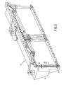
- Figs. 1 and 2 show a device 1 for placing components on a printed circuit board in lateral elevation and in plan view, respectively.
- the reference numeral 2 in these Figures indicates a printed circuit board which has already been provided with components 3 at the lower side, which components have been placed in holes in the printed circuit board 2 with their connection wires.
- the printed circuit board 2 is supported by a carrier 5.
- Components are yet to be placed on the upper side of the printed circuit board 2. These may be: components suitable for surface mounting, the so-called SMDs such as PLCCs, QFPs, SOTs, etc., or components having connection wires which are to be inserted in holes in the printed circuit board 2.
- the components must be placed on the printed circuit board 2 in an accurate manner with small mutual inter- spacings.
- the components to be placed are packed in known manner in packaging tapes 9 wound on reels 7.
- the packaging tape 9 comprises a carrier tape 11 with compartments and a covering tape 13.
- the covering tape 13 is removed from the carrier tape 11 and the components accommodated in the compartments may be taken from the carrier tape 11 in a feed position 15.
- the components are taken from the feed positions 15 and put on the printed circuit board 2 by a transfer mechanism 17.
- the transfer mechanism 17 comprises a slide 19 which can be displaced in an x-direction and a pick-up device 21 which is also constructed as a slide and which can be displaced in a y-direction.
- the pick-up device 21 is provided with a number of manipulators 23 which are capable of picking up components by means of an underpressure and which are each rotatable about a z-axis which is transverse to the x- and y-directions.
- manipulators 23 are positioned in the pick-up device 21 in a pattern which corresponds to the pattern of the feed positions 15, so that the manipulators 23 can pick up components simultaneously.
- the device further comprises an imaging device 25 which is situated between the feed positions 15 and the printed circuit board 2.
- the imaging device comprises a known video camera, a flash gun and an optical system (not shown). Pictures can be taken by the camera 25 of objects which are present in the image field 27 situated above the camera.
- Fig. 3 shows a pick-up device 21 which corresponds to a device as described in detail in a European Patent Application Publication EP-A1 0434156 by Applicant (Application no. 90203353.9).
- Each cylindrical manipulator 23 is rotatable about a centreline 29 and arranged coaxially in a holder 31 which is connected to a frame 33.
- Each manipulator 23 is provided with a coaxially situated channel 35 in which an underpressure can be generated, so that the manipulator 23 can pick up a component.
- the pick-up device 21 is further provided with a reference member 37.
- the reference member 37 is a notch provided in a frame 33 of the pick-up device 21, which notch is essentially black and on which white marks 39 are provided (see Fig. 4).
- the positions of the marks 39 relative to the manipulators 23 are measured and stored in a control system (not shown).
- the transfer mechanism 17 with the manipulators 23 is brought to above the feed positions 15 by the control system. Components are picked up simultaneously or one by one by the manipulators 23 by means of an underpressure. The manipulators 23 are then displaced in the y-direction through the image field 27 over the camera 25. The moment a manipulator 23 is present in the image field 27 of the camera 25 the flash gun is triggered and a picture of the component held by the manipulator and of a portion of the reference member 37 situated in the vicinity of the manipulator is taken. The movements of the transfer mechanism 17 and the manipulators 23, the camera 25 and the flash gun are controlled by the control system. A picture is taken of every component in this manner.
- a picture may be obtained of each component carried by a manipulator 23 and a portion of the reference member 37 in a short time since the pictures of the components are taken while the manipulators 23 are moving over the camera 25, without each manipulator 23 having to be stopped in the image field 27 of the imaging device 25. Deceleration and acceleration forces on the components are avoided by this, and displacements of the component relative to the manipulator 23 as a result of these forces are prevented.
- the reference member 37 may also be constructed as a plate which is fastened to the frame 33 and which is provided with marks against a contrasting background, which plate is directed transversely to the centrelines 29 of the manipulators 23.
- Fig. 5 shows a diagrammatic picture of a component 41 and a portion of the reference member 37 fastened to the frame 33.
- the connection surfaces 43 of the component 41 and the marks 39 of the reference member 37 are clearly visible. It is stored in the control system where the camera 25 is situated relative to the device 1, where the reference member 37 is situated relative to the manipulator 23, as well as a model picture of the connection surfaces 43 of the component 41.
- the position of the reference member 37 relative to the camera 25 at the moment at which the picture was made can be determined from the picture made, after which the position of the manipulator 23 can also be determined.
- the position of the component 41 relative to the camera 25 at the moment at which the picture was made can also be derived from this picture.
- the position of the component 41 relative to the manipulator 23 is implicitly known as a result. This relative position, however, need not be separately computed.
- the control system determines the angular rotation and the displacements to be carried out by the manipulator 23 in such a way that the component 41 is placed on the printed circuit board 2 in the desired position.
- imaging devices such as, for example, linear CCD cameras, photocameras, or laser scanners may be used instead of a video camera.
- Fig. 6a shows a second embodiment of a device 50 according to the invention which is suitable for placing components 51 with connection wires 53 in holes 55 in a printed circuit board 57.
- a device similar to a device 50 but without the main characterizing feature of the invention (reference member 65) is described in detail in a European Patent Application Publication EP-A2 0432848 by Applicant (Application no. 90203234.1).
- the device 50 comprises a robot 59 which is provided with a manipulator 61 which can pick up components by means of grippers 63.
- the manipulator 61 is provided with three legs 65 which act as reference members.
- the robot 59 is controlled by a control system 67.
- the control system 67 is provided with information about the movements to be carried out by the robot 59 by a computer 69.
- the device 50 is further provided with an imaging device 71 (Figs. 6b, 6c) which comprises seven light sources and seven light sensors. A light beam emitted by the light source is detected by a light sensor cooperating with this light source.
- the operation of the device 50 is as follows.
- the component 51 held by the manipulator 61 is moved through the imaging device 71 by the robot 59.
- the legs 65 of the manipulator 61 interrupt the light beams 101, 102 and 103, so that the light sensors temporarily receive no light.
- the moments at which the light beams are interrupted are stored in the computer.
- the moments at which the connection wires 53 of the component 51 interrupt the light beams 104, 105 and 106 are also stored in the computer.
- the light beam 107 is only interrupted if one of the connection wires 53 is too long, so that the computer 69 gives an alarm signs.
- the position of the component 51 relative to the manipulator 61 is computed by the computer 69 from the moments at which the light beams 101 to 106 were interrupted. This may be done in a manner analogous to that described in the cited European Patent Application Publication EP-A2 0432848 (application number 90203234.1) or in the already mentioned US patent 4553843.
- the position of the printed circuit board 57, the positions of the holes 55 and the expected position of the component 51 relative to the manipulator 61 are stored in the computer 69.
- the displacement to be carried out by the manipulator 61 is computed from the position of the manipulator 61 the deviations of the actual position from the expected position of the component 51 relative to the manipulator 61, and the positions of the holes 55 in the printed circuit board 57 in such a way that the connnection wires 53 can be inserted in the holes 55 of the printed circuit board, upon which the component 51 is placed on the printed circuit board 57.
- the position of the printed circuit board 57 relative to the manipulator 61 must be exactly known in order to obtain a correct placement of the component 51.
- the exact position of the imaging device 71 relative to the manipulator 61 and the printed circuit board 57 need not be known because this position plays no part in the determination of the position of the component 51 relative to the manipulator 61 and the printed circuit board 57.
- a picture of the component and of a reference member coupled to the manipulator is used both in the determination of the positions of manipulator and component relative to the imaging device and in the determination of the position of the component relative to the manipulator. Both methods can be used with the devices described above. When determining the positions relative to the imaging device, the position of the imaging device relative to the device must be exactly known.
Abstract
A method of placing a component on a printed circuit board by means of a manipulator and a device suitable for carrying out this method, whereby the position of the component is determined with an imaging device. The imaging device makes a picture of the component and of a reference member coupled to the manipulator. The position of the component relative to the manipulator can be directly determined from this picture. The positions of the manipulator and the component relative to the imaging device may also be determined.
Description
- The invention relates to methods of placing a component on a printed circuit board whereby a manipulator carrying the component is displaced relative to an imaging device and the component is brought into an image field of the imaging device, after which the position of the component is determined by means of the imaging device and subsequently the component is put in the correct position on the printed circuit board by the manipulator. The invention also relates to a device provided with an imaging device and at least one manipulator displaceable relative to the imaging device.
- A method of the kind mentioned in the opening paragraph and a device for carrying out said method are known from German Patent A1 3546216. In this known method, an electronic component (chip) is transported to a feed position by a supply device. In this feed position, a manipulator controlled by a control system pick up the component by means of an underpressure and moves it into an image field of an imaging device. A picture of the component is then taken by means of the imaging device. In an image signal processor, this picture is compared with a model picture of the component stored in this processor, and deviations in an x-and a y-direction and an angular deviation about a z-axis are computed. An x-axis and a y-axis, which define the x- and y-directions, lie in a plane parallel to the printed circuit board on which the component is to be placed. The z-axis is directed transversely to this plane and coincides with an axis of rotation of the manipulator. After the deviations have been computed, the component is rotated through an angle by the manipulator and is put in the desired position on the printed circuit board, during which the computed deviations are taken into account. During imaging of the component it is necessary for the manipulator to be in a position relative to the imaging device which is known beforehand. The position of the manipulator is determined by the control system. If the manipulator moves at a certain speed relative to the imaging device during imaging, the exact position of the manipulator at the imaging moment cannot be accurately determined by means of the control system. A disadvantage of this method and of this device is that, if the manipulator position relative to the imaging device deviates from the expected position, the position of the component relative to the imaging device cannot be well determined, and faulty corrections will be carried out. For example, if the component is picked up eccentrically by the manipulator, a rotation about the z-axis will cause deviations in the x- and y-directions. If the position of the manipulator relative to the imaging device is known, these deviations can be corrected during placement on the printed circuit board. If this position is not accurately known, these deviations cannot be corrected.
- The invention has for its object to provide a method by which the positions of the component and of the manipulator can be accurately determined in such a way that a correct placement on the printed circuit board is possible.
- The method according to the invention is for this purpose characterized in that a picture of the component and of a reference member coupled to the manipulator is made by means of the imaging device, after which the positions of the component and the manipulator relative to the imaging device are determined from this picture. These positions are compared with expected positions relative to the imaging device. Subsequently, the manipulator is moved to above the printed circuit board, during which the deviations are taken into account, and then the component is placed on the printed circuit board in the desired position.
- The invention also has for its object to provide a method by which the position of the component relative to the manipulator can be accurately determined in such a way that a correct placement on the printed circuit board is possible.
- The method according to the invention is for this purpose characterized in that a picture of the component and of a reference member coupled to the manipulator is made by means of the imaging device, after which the position of the component relative to the manipulator is determined from this picture. This relative position is compared with an expected relative position, and deviations in the x-and y-direction and an angular deviation about the z-axis are computed therefrom. The manipulator is then moved to the desired position above the printed circuit board, during which the deviations are taken into account, and then the component is placed on the printed circuit board in the desired position. The position of the manipulator relative to the imaging device must be such that the component and the reference member are in the image field of the imaging device during imaging. The exact position of the imaging device is immaterial in this method.
- It is noted that European Patent A2-0350850 discloses a method and a device where a camera is connected to a manipulator and makes a picture of the component and of a background which moves along with the camera and is provided with marks. In this device, the position of the manipulator relative to the camera is unequivocally known and the problem of determining the component position relative to the manipulator instead of the component position relative to the camera plays no part. A disadvantage of this device is that the camera moves along whenever the manipulator is displaced. The weight of the camera causes positioning inaccuracies during quick movements. Another disadvantage is that the use of a number of manipulators implies that each manipulator must be provided with a separate camera, so that a very expensive device is obtained.
- An embodiment of the method according to the invention is characterized in that a picture is made by the imaging device while the component carried by the manipulator and the reference member coupled to the manipulator are being moved through the image field of the imaging device. This increases the speed at which the component is placed on the printed circuit board. The manipulator may be moved through the image field of the imaging device at any speed desired.
- The invention also has for its object to provide a device by which the disadvantage of the known device is obviated. The device suitable for carrying out the method according to the invention is for this purpose characterized in that the device is provided with a reference member which is coupled to the manipulator. This reference member has a fixed position relative to the manipulator. As a result, the position of the manipulator is known if the position of the reference member has been determined by the imaging device. The position of the component relative to the reference member can also be determined, upon which the position of the component relative to the manipulator is known.
- An embodiment of the device according to the invention is characterized in that the device is provided with a number of manipulators, while the reference member is a common reference member which is coupled to all manipulators. The use of a number of manipulators increases the speed at which components can be placed on a printed circuit board. The use of a common reference member for all manipulators has the advantage that all manipulators can be coupled to a reference member in a simple manner.
- Another embodiment of the device according to the invention is characterized in that the reference member comprises a plate which is provided with at least one mark. The mark may be a white square which is provided on a black plate so as to obtain a good contrast. An inexpensive reference member is obtained in this way which may be added in a simple way to an existing component placement device, such as, for example, the one described in the German Patent A1 3546216.
- A further embodiment of the device according to the invention is characterized in that the reference member comprises a number of legs. Such a reference member is suitable in a device which is also provided with an imaging device which comprises at least one light source and a light sensor cooperating with said light source and which is suitable for placing components having connection wires. The legs of the reference member coupled to the manipulator and the connection wires of the component interrupt a light beam emitted by the light source in the direction of the light sensor at different moments. The position of the component relative to the manipulator can be determined from these moments. Such an imaging device is known from US Patent 4553843.
- The invention will be explained in more detail with reference to the drawing in which
- Fig. 1 is a diagrammatic side elevation of a device according to the invention,
- Fig. 2 is a diagrammatic plan view of the device,
- Fig. 3 shows a pick-up device with a number of manipulators of the device,
- Fig. 4 is a bottom view of the pick-up device depicted in Fig. 3,
- Fig. 5 shows a component with a reference member according to the invention,
- Fig. 6a diagrammatically shows a second embodiment of a device according to the invention, and
- Figs. 6b and 6c are a plan view and a lateral elevation, respectively, of an imaging device belonging to the device shown in Fig. 6a.
- The same reference numerals are used for the corresponding parts in the various Figures.
- Figs. 1 and 2 show a
device 1 for placing components on a printed circuit board in lateral elevation and in plan view, respectively. Thereference numeral 2 in these Figures indicates a printed circuit board which has already been provided withcomponents 3 at the lower side, which components have been placed in holes in the printedcircuit board 2 with their connection wires. The printedcircuit board 2 is supported by acarrier 5. Components are yet to be placed on the upper side of the printedcircuit board 2. These may be: components suitable for surface mounting, the so-called SMDs such as PLCCs, QFPs, SOTs, etc., or components having connection wires which are to be inserted in holes in the printedcircuit board 2. The components must be placed on the printedcircuit board 2 in an accurate manner with small mutual inter- spacings. The components to be placed are packed in known manner inpackaging tapes 9 wound on reels 7. Thepackaging tape 9 comprises acarrier tape 11 with compartments and a coveringtape 13. The coveringtape 13 is removed from thecarrier tape 11 and the components accommodated in the compartments may be taken from thecarrier tape 11 in afeed position 15. The components are taken from the feed positions 15 and put on the printedcircuit board 2 by atransfer mechanism 17. Thetransfer mechanism 17 comprises aslide 19 which can be displaced in an x-direction and a pick-updevice 21 which is also constructed as a slide and which can be displaced in a y-direction. The pick-updevice 21 is provided with a number ofmanipulators 23 which are capable of picking up components by means of an underpressure and which are each rotatable about a z-axis which is transverse to the x- and y-directions. A more detailed description of such adevice 1 which is suitable for placing components on a printedcircuit board 2 can be found in European Patent 92292. Themanipulators 23 are positioned in the pick-updevice 21 in a pattern which corresponds to the pattern of the feed positions 15, so that themanipulators 23 can pick up components simultaneously. The device further comprises animaging device 25 which is situated between the feed positions 15 and the printedcircuit board 2. The imaging device comprises a known video camera, a flash gun and an optical system (not shown). Pictures can be taken by thecamera 25 of objects which are present in theimage field 27 situated above the camera. - Fig. 3 shows a pick-up
device 21 which corresponds to a device as described in detail in a European Patent Application Publication EP-A1 0434156 by Applicant (Application no. 90203353.9). Eachcylindrical manipulator 23 is rotatable about acentreline 29 and arranged coaxially in aholder 31 which is connected to aframe 33. Eachmanipulator 23 is provided with a coaxially situatedchannel 35 in which an underpressure can be generated, so that themanipulator 23 can pick up a component. The pick-updevice 21 is further provided with areference member 37. Thereference member 37 is a notch provided in aframe 33 of the pick-updevice 21, which notch is essentially black and on which white marks 39 are provided (see Fig. 4). The positions of themarks 39 relative to themanipulators 23 are measured and stored in a control system (not shown). - The operation of the
device 1 is now briefly explained. Thetransfer mechanism 17 with themanipulators 23 is brought to above the feed positions 15 by the control system. Components are picked up simultaneously or one by one by themanipulators 23 by means of an underpressure. Themanipulators 23 are then displaced in the y-direction through theimage field 27 over thecamera 25. The moment amanipulator 23 is present in theimage field 27 of thecamera 25 the flash gun is triggered and a picture of the component held by the manipulator and of a portion of thereference member 37 situated in the vicinity of the manipulator is taken. The movements of thetransfer mechanism 17 and themanipulators 23, thecamera 25 and the flash gun are controlled by the control system. A picture is taken of every component in this manner. A picture may be obtained of each component carried by amanipulator 23 and a portion of thereference member 37 in a short time since the pictures of the components are taken while themanipulators 23 are moving over thecamera 25, without eachmanipulator 23 having to be stopped in theimage field 27 of theimaging device 25. Deceleration and acceleration forces on the components are avoided by this, and displacements of the component relative to themanipulator 23 as a result of these forces are prevented. - The
reference member 37 may also be constructed as a plate which is fastened to theframe 33 and which is provided with marks against a contrasting background, which plate is directed transversely to thecentrelines 29 of themanipulators 23. - Fig. 5 shows a diagrammatic picture of a
component 41 and a portion of thereference member 37 fastened to theframe 33. The connection surfaces 43 of thecomponent 41 and themarks 39 of thereference member 37 are clearly visible. It is stored in the control system where thecamera 25 is situated relative to thedevice 1, where thereference member 37 is situated relative to themanipulator 23, as well as a model picture of the connection surfaces 43 of thecomponent 41. The position of thereference member 37 relative to thecamera 25 at the moment at which the picture was made can be determined from the picture made, after which the position of themanipulator 23 can also be determined. The position of thecomponent 41 relative to thecamera 25 at the moment at which the picture was made can also be derived from this picture. When the positions of themanipulator 23 relative to thecamera 25 and of thecomponent 41 relative to thecamera 25 are known, the position of thecomponent 41 relative to themanipulator 23 is implicitly known as a result. This relative position, however, need not be separately computed. The control system then determines the angular rotation and the displacements to be carried out by themanipulator 23 in such a way that thecomponent 41 is placed on the printedcircuit board 2 in the desired position. - Other known imaging devices such as, for example, linear CCD cameras, photocameras, or laser scanners may be used instead of a video camera.
- Fig. 6a shows a second embodiment of a
device 50 according to the invention which is suitable for placingcomponents 51 withconnection wires 53 inholes 55 in a printedcircuit board 57. A device similar to adevice 50 but without the main characterizing feature of the invention (reference member 65) is described in detail in a European Patent Application Publication EP-A2 0432848 by Applicant (Application no. 90203234.1). Thedevice 50 comprises arobot 59 which is provided with amanipulator 61 which can pick up components by means ofgrippers 63. Themanipulator 61 is provided with threelegs 65 which act as reference members. Therobot 59 is controlled by acontrol system 67. Thecontrol system 67 is provided with information about the movements to be carried out by therobot 59 by acomputer 69. Thedevice 50 is further provided with an imaging device 71 (Figs. 6b, 6c) which comprises seven light sources and seven light sensors. A light beam emitted by the light source is detected by a light sensor cooperating with this light source. The operation of thedevice 50 is as follows. Thecomponent 51 held by themanipulator 61 is moved through theimaging device 71 by therobot 59. Thelegs 65 of themanipulator 61 interrupt the light beams 101, 102 and 103, so that the light sensors temporarily receive no light. The moments at which the light beams are interrupted are stored in the computer. The moments at which theconnection wires 53 of thecomponent 51 interrupt the light beams 104, 105 and 106 are also stored in the computer. Thelight beam 107 is only interrupted if one of theconnection wires 53 is too long, so that thecomputer 69 gives an alarm signs. The position of thecomponent 51 relative to themanipulator 61 is computed by thecomputer 69 from the moments at which the light beams 101 to 106 were interrupted. This may be done in a manner analogous to that described in the cited European Patent Application Publication EP-A2 0432848 (application number 90203234.1) or in the already mentioned US patent 4553843. The position of the printedcircuit board 57, the positions of theholes 55 and the expected position of thecomponent 51 relative to themanipulator 61 are stored in thecomputer 69. - The displacement to be carried out by the
manipulator 61 is computed from the position of themanipulator 61 the deviations of the actual position from the expected position of thecomponent 51 relative to themanipulator 61, and the positions of theholes 55 in the printedcircuit board 57 in such a way that theconnnection wires 53 can be inserted in theholes 55 of the printed circuit board, upon which thecomponent 51 is placed on the printedcircuit board 57. The position of the printedcircuit board 57 relative to themanipulator 61 must be exactly known in order to obtain a correct placement of thecomponent 51. The exact position of theimaging device 71 relative to themanipulator 61 and the printedcircuit board 57 need not be known because this position plays no part in the determination of the position of thecomponent 51 relative to themanipulator 61 and the printedcircuit board 57. - A picture of the component and of a reference member coupled to the manipulator is used both in the determination of the positions of manipulator and component relative to the imaging device and in the determination of the position of the component relative to the manipulator. Both methods can be used with the devices described above. When determining the positions relative to the imaging device, the position of the imaging device relative to the device must be exactly known.
Claims (7)
1. A method of placing a component on a printed circuit board whereby a manipulator carrying the component is displaced relative to an imaging device and the component is brought into an image field of the imaging device, after which the position of the component is determined by means of the imaging device and subsequently the component is put in the correct position on the printed circuit board by the manipulator, characterized in that a picture of the component and of a reference member coupled to the manipulator is made by means of the imaging device, after which the positions of the component and the manipulator relative to the imaging device are determined from this picture.
2. A method of placing a component on a printed circuit board whereby a manipulator carrying the component is displaced relative to an imaging device and the component is brought into an image field of the imaging device, after which the position of the component is determined by means of the imaging device and subsequently the component is put in the correct position on the printed circuit board by the manipulator, characterized in that a picture of the component and of a reference member coupled to the manipulator is made by means of the imaging device, after which the position of the component relative to the manipulator is determined from this picture.
3. A method as claimed in Claim 1 or 2, characterized in that a picture is made by the imaging device while the component carried by the manipulator and the reference member coupled to the manipulator are being moved through the image field of the imaging device.
4. A device suitable for carrying out the method as claimed in Claim 1, 2 or 3, provided with an imaging device and at least one manipulator which is displaceable relative to the imaging device, characterized in that the device is provided with a reference member which is coupled to the manipulator.
5. A device as claimed in Claim 4, characterized in that the device is provided with a number of manipulators, while the reference member is a common reference member which is coupled to all manipulators.
6. A device as claimed in Claim 4 or 5, characterized in that the reference member comprises a plate which is provided with at least one mark.
7. A device as claimed in Claim 4 or 5, characterized in that the reference member comprises a number of legs.
Applications Claiming Priority (2)
| Application Number | Priority Date | Filing Date | Title |
|---|---|---|---|
| EP91201206 | 1991-05-21 | ||
| EP91201206 | 1991-05-21 |
Publications (1)
| Publication Number | Publication Date |
|---|---|
| EP0514975A1 true EP0514975A1 (en) | 1992-11-25 |
Family
ID=8207658
Family Applications (1)
| Application Number | Title | Priority Date | Filing Date |
|---|---|---|---|
| EP92201352A Ceased EP0514975A1 (en) | 1991-05-21 | 1992-05-12 | Methods of placing a component on a printed circuit board, and device suitable for carrying out said methods |
Country Status (3)
| Country | Link |
|---|---|
| US (1) | US5216804A (en) |
| EP (1) | EP0514975A1 (en) |
| JP (1) | JPH05198994A (en) |
Cited By (3)
| Publication number | Priority date | Publication date | Assignee | Title |
|---|---|---|---|---|
| BE1007587A3 (en) * | 1993-09-23 | 1995-08-16 | Philips Electronics Nv | Method for the placement of an object in a desired location on a carrier aswell as the device suitable for the carrying out of such a method and objectsuitable for application of such a method |
| US6332269B1 (en) | 1997-08-21 | 2001-12-25 | Micron Technology, Inc. | Component alignment methods |
| WO2005013665A1 (en) * | 2003-08-04 | 2005-02-10 | Assembleon N.V. | Component placement device and method |
Families Citing this family (11)
| Publication number | Priority date | Publication date | Assignee | Title |
|---|---|---|---|---|
| JP3114034B2 (en) * | 1992-06-05 | 2000-12-04 | ヤマハ発動機株式会社 | Component mounting method and component mounting device |
| JP2554431B2 (en) * | 1992-11-05 | 1996-11-13 | ヤマハ発動機株式会社 | Mounting device component suction state detection device |
| US5479694A (en) * | 1993-04-13 | 1996-01-02 | Micron Technology, Inc. | Method for mounting integrated circuits onto printed circuit boards and testing |
| US5455894A (en) * | 1993-04-19 | 1995-10-03 | Advanced Micro Devices | Wafer fabrication robotic interface unit |
| JP3339230B2 (en) * | 1995-01-17 | 2002-10-28 | 松下電器産業株式会社 | Apparatus and method for supporting printed circuit board and mounting apparatus |
| EP0809926B1 (en) * | 1995-12-14 | 1999-11-10 | Koninklijke Philips Electronics N.V. | Component placement machine |
| EP0811310A1 (en) * | 1995-12-14 | 1997-12-10 | Koninklijke Philips Electronics N.V. | Method of placing a component on a carrier, and component placement machine for implementing said method |
| US6157866A (en) * | 1997-06-19 | 2000-12-05 | Advanced Micro Devices, Inc. | Automated material handling system for a manufacturing facility divided into separate fabrication areas |
| JP5098846B2 (en) * | 2008-06-23 | 2012-12-12 | 富士電機株式会社 | Robot system |
| JP5223683B2 (en) * | 2009-01-05 | 2013-06-26 | 富士電機株式会社 | Work holding position and orientation measurement system and work transfer system |
| JP5381147B2 (en) * | 2009-02-17 | 2014-01-08 | 富士電機株式会社 | Work transfer system |
Citations (8)
| Publication number | Priority date | Publication date | Assignee | Title |
|---|---|---|---|---|
| US4472056A (en) * | 1980-07-23 | 1984-09-18 | Hitachi, Ltd. | Shape detecting apparatus |
| US4553843A (en) * | 1981-08-03 | 1985-11-19 | Micro Component Technology, Inc. | Apparatus for determining the alignment of leads on a body |
| DE3546216A1 (en) * | 1984-12-26 | 1986-07-03 | TDK Corporation, Tokio/Tokyo | DEVICE FOR FASTENING ELECTRONIC COMPONENTS ON PRINTED CIRCUIT BOARDS |
| EP0284381A2 (en) * | 1987-03-24 | 1988-09-28 | Emhart Inc. | Lead sense system for component insertion machine |
| EP0350850A2 (en) * | 1988-07-14 | 1990-01-17 | ROHDE & SCHWARZ ENGINEERING AND SALES GMBH | Device for the insertion of components in printed circuits by machine |
| EP0394568A1 (en) * | 1987-11-02 | 1990-10-31 | Mpm Corp. | Video probe aligning of object to be acted upon |
| EP0432848A2 (en) * | 1989-12-13 | 1991-06-19 | Koninklijke Philips Electronics N.V. | Apparatus for sensing a position of a lead of a component |
| EP0434156A1 (en) * | 1989-12-21 | 1991-06-26 | Koninklijke Philips Electronics N.V. | Device comprising at least two manipulators, positioning device suitable for placing electrical components on a support and pick-up device suitable for use in such a positioning device |
Family Cites Families (9)
| Publication number | Priority date | Publication date | Assignee | Title |
|---|---|---|---|---|
| JPS57189703A (en) * | 1981-05-15 | 1982-11-22 | Sumitomo Electric Ind Ltd | Cutting tool |
| NL8201653A (en) * | 1982-04-21 | 1983-11-16 | Philips Nv | METHOD AND APPARATUS FOR PLACING CHIP-SHAPED ELECTRICAL AND / OR ELECTRONIC COMPONENTS ON A SUBSTRATE |
| EP0144717B1 (en) * | 1983-11-05 | 1988-10-19 | Zevatech AG | Method and device positioning elements on a work piece |
| JPS63260280A (en) * | 1987-04-16 | 1988-10-27 | Mitsubishi Electric Corp | Electronic component mount device |
| GB2223429B (en) * | 1988-08-24 | 1993-02-17 | Tdk Corp | Apparatus for and method of automatically mounting electronic component on printed circuit board |
| JP2776860B2 (en) * | 1989-01-11 | 1998-07-16 | 株式会社日立製作所 | Electronic component mounting device and mounting method |
| US5177864A (en) * | 1989-09-06 | 1993-01-12 | Matsushita Electric Industrial Co., Ltd. | Electronic component mounting apparatus and method of mounting electronic component |
| JP2803221B2 (en) * | 1989-09-19 | 1998-09-24 | 松下電器産業株式会社 | IC mounting apparatus and method |
| US4980971A (en) * | 1989-12-14 | 1991-01-01 | At&T Bell Laboratories | Method and apparatus for chip placement |
-
1991
- 1991-10-03 US US07/771,387 patent/US5216804A/en not_active Expired - Fee Related
-
1992
- 1992-05-12 EP EP92201352A patent/EP0514975A1/en not_active Ceased
- 1992-05-20 JP JP4127409A patent/JPH05198994A/en active Pending
Patent Citations (8)
| Publication number | Priority date | Publication date | Assignee | Title |
|---|---|---|---|---|
| US4472056A (en) * | 1980-07-23 | 1984-09-18 | Hitachi, Ltd. | Shape detecting apparatus |
| US4553843A (en) * | 1981-08-03 | 1985-11-19 | Micro Component Technology, Inc. | Apparatus for determining the alignment of leads on a body |
| DE3546216A1 (en) * | 1984-12-26 | 1986-07-03 | TDK Corporation, Tokio/Tokyo | DEVICE FOR FASTENING ELECTRONIC COMPONENTS ON PRINTED CIRCUIT BOARDS |
| EP0284381A2 (en) * | 1987-03-24 | 1988-09-28 | Emhart Inc. | Lead sense system for component insertion machine |
| EP0394568A1 (en) * | 1987-11-02 | 1990-10-31 | Mpm Corp. | Video probe aligning of object to be acted upon |
| EP0350850A2 (en) * | 1988-07-14 | 1990-01-17 | ROHDE & SCHWARZ ENGINEERING AND SALES GMBH | Device for the insertion of components in printed circuits by machine |
| EP0432848A2 (en) * | 1989-12-13 | 1991-06-19 | Koninklijke Philips Electronics N.V. | Apparatus for sensing a position of a lead of a component |
| EP0434156A1 (en) * | 1989-12-21 | 1991-06-26 | Koninklijke Philips Electronics N.V. | Device comprising at least two manipulators, positioning device suitable for placing electrical components on a support and pick-up device suitable for use in such a positioning device |
Cited By (10)
| Publication number | Priority date | Publication date | Assignee | Title |
|---|---|---|---|---|
| BE1007587A3 (en) * | 1993-09-23 | 1995-08-16 | Philips Electronics Nv | Method for the placement of an object in a desired location on a carrier aswell as the device suitable for the carrying out of such a method and objectsuitable for application of such a method |
| US6332269B1 (en) | 1997-08-21 | 2001-12-25 | Micron Technology, Inc. | Component alignment methods |
| US6463653B1 (en) | 1997-08-21 | 2002-10-15 | Micron Technology, Inc. | Component alignment apparatuses |
| US6606791B1 (en) | 1997-08-21 | 2003-08-19 | Micron Technology, Inc. | Component alignment methods |
| US6845555B1 (en) | 1997-08-21 | 2005-01-25 | Micron Technology, Inc. | Component alignment methods |
| US6895661B1 (en) | 1997-08-21 | 2005-05-24 | Micron Technology, Inc. | Component alignment apparatuses and methods |
| US7017262B1 (en) | 1997-08-21 | 2006-03-28 | Micron Technology, Inc. | Component alignment methods |
| US7222414B2 (en) | 1997-08-21 | 2007-05-29 | Micron Technology, Inc. | Component transfer systems |
| WO2005013665A1 (en) * | 2003-08-04 | 2005-02-10 | Assembleon N.V. | Component placement device and method |
| US7272887B2 (en) | 2003-08-04 | 2007-09-25 | Assembleon N.V. | Component placement device and method |
Also Published As
| Publication number | Publication date |
|---|---|
| US5216804A (en) | 1993-06-08 |
| JPH05198994A (en) | 1993-08-06 |
Similar Documents
| Publication | Publication Date | Title |
|---|---|---|
| US5768759A (en) | Method and apparatus for reflective in-flight component registration | |
| US5724722A (en) | Part state detecting device for mounter | |
| US5216804A (en) | Method and device for placing a component on a printed circuit board | |
| KR910003000B1 (en) | Electronic component mounting system | |
| US6506614B1 (en) | Method of locating and placing eye point features of a semiconductor die on a substrate | |
| US5467186A (en) | Attracting nozzle control apparatus for a chip component mounting machine | |
| US5249356A (en) | Method and apparatus for mounting electronic component | |
| US7089656B2 (en) | Electric parts mounting apparatus | |
| US7181089B2 (en) | Method and apparatus for searching for fiducial marks, and method of detecting positions of the fiducial marks | |
| US6043877A (en) | Calibration carrier for a component placement machine having an adhesive reflective surface | |
| KR101506519B1 (en) | Component mounting apparatus | |
| US6853874B2 (en) | Variable-width substrate conveyor, method of changing width of the same, and method of matching widths of two adjacent substrate conveyors | |
| JP4516220B2 (en) | Relative positional relationship acquisition method and electrical component mounting system for component mounting accuracy related parts | |
| US4922434A (en) | Linear interpolation for a component placement robot | |
| EP1154227B1 (en) | Edge detecting method and edge detecting apparatus | |
| EP0809926B1 (en) | Component placement machine | |
| US20020111709A1 (en) | Apparatus and method for determining a reference position for an industrial robot | |
| KR20010074993A (en) | Method and device for processing substrates | |
| US6195454B1 (en) | Component mounting apparatus | |
| US20020071601A1 (en) | Apparatus for detecting lead coplanarity, apparatus for detecting condition of electronic component, and system for mounting electronic component | |
| EP0341629B1 (en) | Printed circuit board and a method of recognizing the position of surface mounted parts | |
| JP4562275B2 (en) | Electrical component mounting system and accuracy inspection method thereof | |
| JPH11121992A (en) | Working apparatus and electronic circuit device mounting apparatus | |
| JPH08236997A (en) | Method of correcting mounting position of mounting device | |
| WO1997022237A1 (en) | Method of placing a component on a carrier, and component placement machine for implementing said method |
Legal Events
| Date | Code | Title | Description |
|---|---|---|---|
| PUAI | Public reference made under article 153(3) epc to a published international application that has entered the european phase |
Free format text: ORIGINAL CODE: 0009012 |
|
| AK | Designated contracting states |
Kind code of ref document: A1 Designated state(s): DE FR GB |
|
| 17P | Request for examination filed |
Effective date: 19930517 |
|
| 17Q | First examination report despatched |
Effective date: 19941123 |
|
| STAA | Information on the status of an ep patent application or granted ep patent |
Free format text: STATUS: THE APPLICATION HAS BEEN REFUSED |
|
| K1C1 | Correction of patent application (title page) published |
Effective date: 19921125 |
|
| 18R | Application refused |
Effective date: 19950518 |