EP0508395B1 - Grounding device - Google Patents
Grounding device Download PDFInfo
- Publication number
- EP0508395B1 EP0508395B1 EP92106059A EP92106059A EP0508395B1 EP 0508395 B1 EP0508395 B1 EP 0508395B1 EP 92106059 A EP92106059 A EP 92106059A EP 92106059 A EP92106059 A EP 92106059A EP 0508395 B1 EP0508395 B1 EP 0508395B1
- Authority
- EP
- European Patent Office
- Prior art keywords
- circuit board
- contact
- tab
- arrangement according
- earthing
- Prior art date
- Legal status (The legal status is an assumption and is not a legal conclusion. Google has not performed a legal analysis and makes no representation as to the accuracy of the status listed.)
- Expired - Lifetime
Links
- 210000002105 tongue Anatomy 0.000 claims abstract description 10
- 239000004020 conductor Substances 0.000 claims description 9
- 239000002184 metal Substances 0.000 claims description 7
- 238000003825 pressing Methods 0.000 claims description 2
- 238000005476 soldering Methods 0.000 claims description 2
- 230000006835 compression Effects 0.000 abstract 1
- 238000007906 compression Methods 0.000 abstract 1
- 238000004519 manufacturing process Methods 0.000 description 3
- 229910001369 Brass Inorganic materials 0.000 description 2
- 239000010951 brass Substances 0.000 description 2
- 239000003990 capacitor Substances 0.000 description 1
- 238000011161 development Methods 0.000 description 1
- 230000018109 developmental process Effects 0.000 description 1
- 238000000034 method Methods 0.000 description 1
- 238000004080 punching Methods 0.000 description 1
Images

Classifications
-
- H—ELECTRICITY
- H02—GENERATION; CONVERSION OR DISTRIBUTION OF ELECTRIC POWER
- H02B—BOARDS, SUBSTATIONS OR SWITCHING ARRANGEMENTS FOR THE SUPPLY OR DISTRIBUTION OF ELECTRIC POWER
- H02B1/00—Frameworks, boards, panels, desks, casings; Details of substations or switching arrangements
- H02B1/16—Earthing arrangements
-
- H—ELECTRICITY
- H01—ELECTRIC ELEMENTS
- H01R—ELECTRICALLY-CONDUCTIVE CONNECTIONS; STRUCTURAL ASSOCIATIONS OF A PLURALITY OF MUTUALLY-INSULATED ELECTRICAL CONNECTING ELEMENTS; COUPLING DEVICES; CURRENT COLLECTORS
- H01R12/00—Structural associations of a plurality of mutually-insulated electrical connecting elements, specially adapted for printed circuits, e.g. printed circuit boards [PCB], flat or ribbon cables, or like generally planar structures, e.g. terminal strips, terminal blocks; Coupling devices specially adapted for printed circuits, flat or ribbon cables, or like generally planar structures; Terminals specially adapted for contact with, or insertion into, printed circuits, flat or ribbon cables, or like generally planar structures
- H01R12/50—Fixed connections
- H01R12/51—Fixed connections for rigid printed circuits or like structures
- H01R12/55—Fixed connections for rigid printed circuits or like structures characterised by the terminals
- H01R12/58—Fixed connections for rigid printed circuits or like structures characterised by the terminals terminals for insertion into holes
Definitions
- the invention relates to an arrangement for ground connection in electronic ballasts for lights or the like, comprising a metallic base part in the form of a U-frame and a printed circuit board equipped with electrical components, the ground connection from a corresponding conductor surface of the printed circuit board via an upward provided on the base part protruding tab takes place, the upper end of which protrudes through an opening in the circuit board.
- the ground connection is further established by fastening the base part to a lamp housing.
- Ballasts such as those used for luminaires equipped with fluorescent lamps, make up a very large proportion of the manufacturing costs of the entire luminaire. It is therefore desirable to minimize manufacturing costs as much as possible.
- the ground connection must always be guaranteed. This means that expensive manual work such as the production of screw connections should be avoided.
- the known design means that the conductor surface, which must be connected to ground, must be located in the area of the opening. However, this imposes restrictions on the course of the conductor tracks on the circuit board. In addition, in order to ensure safe ground contact, the entire resilient pressing member is required, which means that an additional operation is required, which as a rule cannot be automated.
- the object is achieved by a grounding part fastened like an electrical component in the printed circuit board and conductively connected to the ground printed circuit board, which has a contact element which, when inserted into the printed circuit board, projects into the area of the opening of the printed circuit board such that when the PCB in the bottom part of the contact element at the upper end of the tab is pressed.
- the main advantage of the procedure according to the application can be seen in the fact that the contact element, like the electrical components, can be arranged on the circuit board with the same operation.
- the assembly of the printed circuit board with the electrical components and the subsequent electrical connection with the conductor tracks, namely soldering, takes place automatically. Additional measures are not necessary; if necessary, the printed circuit board can even be inserted into the base part by a machine.
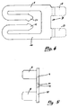
- FIG. 1 shows a cross section through an electronic ballast for lights of the usual type. It has a bottom part 1 designed as a U-frame, in which a printed circuit board 2 is supported.
- the supports for this are not shown in detail. For this purpose it can be tabs fastened to the base part 1 or bent up from it, which have narrow upper ends and shoulders in their course.
- the circuit board 2 rests on openings, recesses or the like on these shoulders. The upper ends projecting through these openings, recesses and the like can be bent beyond the circuit board 2 and thus fix the circuit board in its position.
- the circuit board 2 can, however, also be supported in another way.
- a transformer 3 is provided, cf. Fig.2, is arranged next to the circuit board 2 in this embodiment.
- the printed circuit board 2 is partially supported on the transformer 3 (cf. also FIG. 3).
- the elements arranged in the base part 1, namely the printed circuit board 2 and the transformer 3, are covered by a cover part 4.
- the cover part 4 can consist of plastic or metal and surround the base part 1 on all sides or partially. The metal base part 1 and the cover part 4 thus form a housing.
- the circuit board 2 has a slot-like opening 5 in its end section facing the transformer 3. From the bottom of the bottom part 1, a tab 6 projects upwards through this opening 5 of the printed circuit board 2.
- a grounding part 7 shown in FIGS. 4 and 5 is fastened, in particular soldered, via contact tabs 8 in the printed circuit board 2, in such a way that the contact tabs 8 are soldered to those conductor surfaces (not shown) of the printed circuit board 2 with which the ground connection is made should be done.
- two contact tongues 9 and 10 protrude from the attachment point of the earthing part 7 via its contact lugs 8 in the direction of the opening 5.
- Both contact tongues 9, 10 are bent back inwards again in the plane mentioned, the tips 11 and 12 of the two contact tongues 9 and 10 lie opposite each other via a gap which, when not inserted into the base part 1, is smaller than the thickness of the tab 6.
- These tips 11 and 12 are further provided in the area of the opening 5 of the circuit board in such a way that they are arranged in the area of the tab 6 when the circuit board 2 is inserted into the base part 1 and come into resilient contact against the tab 6 when the tips 11 and 12 are pushed apart.
- the earthing part 7 is made from a flat sheet metal stamped part made of tinned brass, only the lugs forming the contact tabs 8 being bent through 90 ° to the plane of the sheet metal stamped part.
- This grounding part 7 can be handled in the same way as electronic and electrical components by means of an automatic assembly machine and can therefore be brought into mechanical as well as electrical connection when the circuit board 2 is automatically equipped with the circuit board 2. This makes it possible to provide the grounding part 7 at any desired location on the printed circuit board 2. It can also be provided several times. In addition, for this reason it is easy to change the arrangement of the various components on the printed circuit board 2, even at short notice, provided that it is only ensured that a tab 6 protruding through an opening 5 in the printed circuit board 2 is provided on the base part 1.
- This tab 6 can be fastened there or bent upwards after punching out, that is to say form a so-called tear-up part.
- the tab 6 can also be one of the mentioned supports of the printed circuit board 2 and thus have a shoulder (not shown).
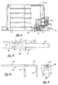
- FIG. 6 shows a different embodiment in partial section, the same elements being designated by the same reference symbols.
- the metal base part 1 which is also designed in the manner of a U-shaped frame, also has a cover 4.
- a circuit board 2 is also provided in the housing thus formed.
- a tab 6 likewise protrudes upward from the bottom part 1, namely also through an opening 5 in the printed circuit board 2, which, in contrast to the exemplary embodiment according to FIGS. 1 to 3, is not slit-shaped but has a closed contour.
- a separate grounding part 17 is provided, which is fastened in the printed circuit board 2 via contact lugs 18, in the exemplary embodiment 4 contact lugs 18, namely soldered on. 7 to 9, contact tongues are not provided here, but a slot 19 is provided, the width of which is somewhat less than the thickness of the tab 6.
- the upper end 20 of the tab 6 penetrates through the slot 19 and presses against the side surfaces 20, 21 and thus achieves reliable electrical contact.
- a pin-like contact extension 22 projecting in a plane parallel to the printed circuit board is additionally provided on the grounding part 17, which protrudes beyond the printed circuit board 2 in the installed state of the grounding part 17 (FIG. 6) and thus connects to one part in a front part 23 of the housing provided terminal 24.
- This embodiment is particularly expedient if the ground connection to the lamp is not made via a screw connection of the base part to the lamp but via a terminal connection or if a terminal connection is to be provided for other reasons.
- the grounding part 17 is also a sheet-metal stamped part made of tinned brass, the four contact tabs 18 here still having to be bent (FIG. 8, FIG. 9).
- the second embodiment of the grounding part is suitable for automatic assembly.
- the tab 6 of the base part 1 used for the ground connection can also be a supporting element for the printed circuit board 2. This does not necessarily have to be the case.
- the support can also take place in a different way, for example via a corresponding support part 3a of the transformer 3 of the first exemplary embodiment (FIGS. 1 to 3) and / or via a corresponding design of the end part 23, these two parts expediently made of plastic exist and are therefore inexpensive manufactured parts.
Landscapes
- Engineering & Computer Science (AREA)
- Power Engineering (AREA)
- Structures For Mounting Electric Components On Printed Circuit Boards (AREA)
- Arrangement Of Elements, Cooling, Sealing, Or The Like Of Lighting Devices (AREA)
- Waveguide Aerials (AREA)
- Communication Cables (AREA)
Abstract
Description
Die Erfindung betrifft eine Anordnung zur Masseverbindung bei elektronischen Vorschaltgeräten für Leuchten oder dergleichen, aufweisend ein metallisches Bodenteil in Form eines U-Rahmens und eine mit elektrischen Bauteilen bestückte Leiterplatte, wobei die Masseverbindung von einer entsprechenden Leiterfläche der Leiterplatte aus über eine am Bodenteil vorgesehene nach oben wegragende Lasche erfolgt, deren Oberende durch eine Öffnung der Leiterplatte hindurchragt.The invention relates to an arrangement for ground connection in electronic ballasts for lights or the like, comprising a metallic base part in the form of a U-frame and a printed circuit board equipped with electrical components, the ground connection from a corresponding conductor surface of the printed circuit board via an upward provided on the base part protruding tab takes place, the upper end of which protrudes through an opening in the circuit board.
Ausgehend von dieser Anwendung, die meist noch einen Deckel aufweist, und so die elektrischen Bauelemente auf der Leiterplatte in ein Gehäuse einschließt, wird weiter die Masseverbindung über die Befestigung des Bodenteils an einem Leuchtengehäuse herbeigeführt.Proceeding from this application, which usually still has a cover and thus encloses the electrical components on the printed circuit board in a housing, the ground connection is further established by fastening the base part to a lamp housing.
Vorschaltgeräte, wie sie für mit Leuchtstofflampen versehene Leuchten verwendet werden, bedingen einen sehr großen Anteil an den Herstellkosten der gesamten Leuchte. Es ist daher erwünscht, die Herstellkosten weitgehend zu minimieren. Andererseits muß stets die Masseverbindung gewährleistet werden. Dies bedeutet, daß aufwendige Handarbeit wie die Herstellung von Schraubverbindungen vermieden werden soll.Ballasts, such as those used for luminaires equipped with fluorescent lamps, make up a very large proportion of the manufacturing costs of the entire luminaire. It is therefore desirable to minimize manufacturing costs as much as possible. On the other hand, the ground connection must always be guaranteed. This means that expensive manual work such as the production of screw connections should be avoided.
Bei einer Lösung dieses Problems ist vorgeschlagen (DE-GM 89 09 517), den aus dem Bodenteil hochgebogenen Laschen eine besondere Ausführungsform zu geben, derart, daß Schultern gebildet sind und die Leiterfläche der Leiterplatte, die mit Masse zu verbinden ist, in Anlage gegen diese Schultern zu bringen. Vorzugsweise wird dies mittels eines als Federmutter bezeichneten Andrückgliedes, das über das durch die Öffnung hinausragende Oberende der Lasche geschoben werden muß, sichergestellt.In a solution to this problem it is proposed (DE-GM 89 09 517) to give the tabs bent up from the bottom part a special embodiment in such a way that shoulders are formed and the conductor surface of the printed circuit board, which is to be connected to ground, is in contact with the system to bring those shoulders. This is preferably ensured by means of a pressure member, referred to as a spring nut, which has to be pushed over the upper end of the tab protruding through the opening.
Die bekannte Ausgestaltung bedingt, daß die Leiterfläche, die mit Masse in Verbindung gebracht werden muß, sich unbedingt im Bereich der Öffnung befinden muß. Jedoch sind hierdurch Einschränkungen für den Verlauf der Leiterbahnen auf der Leiterplatte gegeben. Außerdem ist, um den sicheren Massekontakt zu gewährleisten ist das gesamte federnde Andrückglied erforderlich, wodurch ein zusätzlicher Arbeitsgang erforderlich ist, der in aller Regel nicht automatisierbar ist.The known design means that the conductor surface, which must be connected to ground, must be located in the area of the opening. However, this imposes restrictions on the course of the conductor tracks on the circuit board. In addition, in order to ensure safe ground contact, the entire resilient pressing member is required, which means that an additional operation is required, which as a rule cannot be automated.
Ausgehend hiervon ist es Aufgabe der vorliegenden Erfindung, eine entsprechende Anordnung so weiterzubilden, daß in einfacher Weise ein sicherer Massekontakt auch ohne zusätzliche Arbeitsgänge bei der Montage gewährleistet werden kann.Based on this, it is an object of the present invention to develop a corresponding arrangement so that a safe ground contact can be ensured in a simple manner even without additional operations during assembly.
Die Aufgabe wird durch ein wie ein elektrisches Bauteil in der Leiterplatte befestigtes und mit der Masse-Leiterplatte leitend verbundenes Erdungsteil gelöst, das ein Kontaktelement aufweist, das bei in die Leiterplatte eingesetztem Zustand so in den Bereich der Öffnung der Leiterplatte ragt, daß bei Einsetzen der Leiterplatte in das Bodenteil das Kontaktelement am Oberende der Lasche unter Anpressung anliegt.The object is achieved by a grounding part fastened like an electrical component in the printed circuit board and conductively connected to the ground printed circuit board, which has a contact element which, when inserted into the printed circuit board, projects into the area of the opening of the printed circuit board such that when the PCB in the bottom part of the contact element at the upper end of the tab is pressed.
Weiterbildungen der Erfindung ergeben sich aus den Unteransprüche.Further developments of the invention result from the subclaims.
Der wesentliche Vorteil der anmeldungsgemäßen Vorgehensweise ist darin zu sehen, daß das Kontaktelement wie die elektrischen Bauteile mit dem gleichen Arbeitsgang auf der Leiterplatte angeordnet werden können. Bei industriell gefertigten Produkten, wie es Vorschaltelemente sind, erfolgt die Bestückung der Leiterplatte mit den elektrischen Bauteilen sowie die anschließende elektrische Verbindung mit den Leiterbahnen, nämlich das Verlöten, automatisch. Zusätzliche Maßnahmen sind nicht erforderlich, ggfs. kann die bestückte Leiterplatte sogar von einem Automaten in das Bodenteil eingesetzt werden.The main advantage of the procedure according to the application can be seen in the fact that the contact element, like the electrical components, can be arranged on the circuit board with the same operation. In the case of industrially manufactured products, such as ballast elements, the assembly of the printed circuit board with the electrical components and the subsequent electrical connection with the conductor tracks, namely soldering, takes place automatically. Additional measures are not necessary; if necessary, the printed circuit board can even be inserted into the base part by a machine.
Die Erfindung wird anhand der in der Zeichnung dargestellten Ausführungsbeispiele näher erläutert. Es zeigen
- Fig.1.
- einen Querschnitt,
- Fig.2.
- einen Längsschnitt und
- Fig.3.
- eine Aufsicht durch bzw. auf ein Vorschaltgerät, bei dem ein Erdungsteil gem. einer ersten Ausführungsform verwendet ist;
- Fig.4.
- in Aufsicht und
- Fig. 5
- in Seitenansicht das Erdungsteil gem. dem ersten Ausführungsbeispiel;
- Fig.6
- im Teil-Längsschnitt ein Vorschaltgerät mit einem Erdungsteil gem. einer zweiten Ausführungsform der Erfindung;
- Fig.7.
- in Aufsicht,
- Fig.8.
- in Seitenansicht und
- Fig.9.
- in Stirnansicht das Erdungsteil gem. dem zweiten Ausführungsbeispiel.
- Fig. 1.
- a cross section,
- Fig. 2.
- a longitudinal section and
- Fig. 3.
- a supervision by or on a ballast in which an earthing part acc. a first embodiment is used;
- Fig. 4.
- under supervision and
- Fig. 5
- in side view the earthing part acc. the first embodiment;
- Fig. 6
- in partial longitudinal section a ballast with an earthing part acc. a second embodiment of the invention;
- Fig. 7.
- under supervision,
- Fig. 8.
- in side view and
- Fig. 9.
- in front view the earthing part acc. the second embodiment.
Fig.1 zeigt einen Querschnitt durch ein elektronisches Vorschaltgerät für Leuchten üblicher Bauart. Es weist ein als U-Rahmen ausgebildetes Bodenteil 1 auf, in dem eine Leiterplatte 2 abstützend gehaltert ist. Die Stützen hierfür sind nicht im einzelnen dargestellt. Es kann sich hierfür um am Bodenteil 1 befestigte oder aus dieser hochgebogene Laschen handeln, die schmale Oberenden aufweisen und in ihrem Verlauf Schultern besitzen. Die Leiterplatte 2 ruht über Öffnungen, Ausnehmungen oder dergleichen auf diesen Schultern. Die durch diese Öffnungen, Ausnehmungen und dergleichen ragenden Oberenden können jenseits der Leiterplatte 2 umgebogen sein und so die Leiterplatte in ihrer Lage fixieren. Die Leiterplatte 2 kann jedoch auch in anderer Weise abgestützt sein.1 shows a cross section through an electronic ballast for lights of the usual type. It has a
Auf der Leiterplatte 2 sind nicht dargestellte elektrische und elektronische Bauelemente wie Widerstände, Kondensatoren und dergleichen, angeordnet. Gemäß Fig.1 ist ein Transformator 3 vorgesehen der, vgl. Fig.2, bei diesem Ausführungsbeispiel neben der Leiterplatte 2 angeordnet ist. Beim Ausführungsbeispiel stützt sich die Leiterplatte 2 zum Teil an dem Transformator 3 ab (vgl. auch Fig.3.). Die in dem Bodenteil 1 angeordneten Elemente, nämlich die bestückte Leiterplatte 2 und der Transformator 3, sind durch ein Deckelteil 4 abgedeckt. Das Deckelteil 4 kann aus Kunststoff oder Metall bestehen und das Bodenteil 1 allseitig oder teilweise umgeben. Das aus Metall bestehende Bodenteil 1 und das Deckelteil 4 bilden so ein Gehäuse.Electrical and electronic components such as resistors, capacitors and the like, not shown, are arranged on the printed
Die Leiterplatte 2 weist in ihrem dem Transformator 3 zugewandten Endabschnitt eine schlitzartige Öffnung 5 auf. Vom Boden des Bodenteils 1 ragt eine Lasche 6 nach oben durch diese Öffnung 5 der Leiterplatte 2 hindurch. Ein in den Fig. 4 und 5 alleine dargestelltes Erdungsteil 7 ist über Kontaktfahnen 8 in der Leiterplatte 2 befestigt insbesondere eingelötet, und zwar derart, daß die Lötverbindung der Kontaktfahnen 8 mit denjenigen Leiterflächen (nicht dargestellt) der Leiterplatte 2 erfolgt, mit denen die Masseverbindung erfolgen soll. Im Wesentlichen parallel zu Erstreckung der Leiterplatte 2 ragen zwei Kontaktzungen 9 und 10 vom Befestigungsort des Erdungsteils 7 über dessen Kontaktfahnen 8 weg in Richtung zur Öffnung 5. Beide Kontaktzungen 9, 10 sind in der erwähnten Ebene nochmals nach innen zurückgebogen, wobei die Spitzen 11 und 12 der beiden Kontaktzungen 9 bzw. 10 sich über einen Spalt gegenübeliegen, der im nicht in das Bodenteil 1 eingesetzten Zustand kleiner ist als die Dicke der Lasche 6. Diese Spitzen 11 und 12 sind weiter derart im Bereich der Öffnung 5 der Leiterplatte vorgesehen, daß sie beim Einsetzen der Leiterplatte 2 in das Bodenteil 1 im Bereich der Lasche 6 angeordnet sind und beim Einführen durch Auseinanderdrücken der Spitzen 11 und 12 in federnde Anlage gegen die Lasche 6 kommen.The
Hierdurch ist eine sichere Masseverbindung erzielt.This ensures a secure earth connection.
Wie sich das insbesondere aus Fig. 4 ergibt, ist das Erdungsteil 7 ausgehend von einem flachen Blech-Stanzteil aus verzinntem Messing hergestellt, wobei lediglich die die Kontaktfahnen 8 bildenden Ansätze um 90° zur Ebene des Blech-Stanzteils umgebogen sind. Dieses Erdungsteil 7 ist in gleicher Weise wie elektronische und elektrische Bauelemente mittels eines Bestückungsautomaten handhabbar und kann daher beim automatischen Bestücken der Leiterplatte 2 mit der Leiterplatte 2 sowohl in mechanische als auch elektrische Verbindung gebracht werden. Hierdurch ist es möglich das Erdungsteil 7 an jedem gewünschten Ort auf der Leiterplatte 2 vorzusehen. Es kann auch mehrfach vorgesehen sein. Darüber hinaus ist es aus diesem Grunde einfach, die Anordnung der verschiedenen Bauelemente auf der Leiterplatte 2, auch kurzfristig, zu ändern, sofern lediglich sichergestellt ist, das eine durch eine Öffnung 5 in der Leiterplatte 2 ragende Lasche 6 am Bodenteil 1 vorgesehen ist.As can be seen in particular from FIG. 4, the earthing
Diese Lasche 6 kann dort befestigt sein oder dort nach Ausstanzen nach oben weggebogen sein, also ein sog. Hochriß-Teil bilden. Die Lasche 6 kann auch eine der erwähnten Stützen der Leiterplatte 2 sein und also eine Schulter aufweisen (nicht dargestellt).This
Fig.6 zeigt im Teilschnitt eine andere Ausführungform, wobei gleiche Elemente mit gleichen Bezugszeichen bezeichnet sind.FIG. 6 shows a different embodiment in partial section, the same elements being designated by the same reference symbols.
Das aus Metall bestehende Bodenteil 1, das ebenfalls nach Art eines U-förmigen Rahmens ausgebildet ist, weist ebenfalls einen Deckel 4 auf. In dem so gebildeten Gehäuse ist ebenfalls eine Leiterplatte 2 vorgesehen. Vom Bodenteil 1 ragt ebenfalls eine Lasche 6 nach oben und zwar ebenfalls durch eine Öffnung 5 in der Leiterplatte 2, die im Gegensatz zum Ausführungsbeispiel gemäß Fig.1 bis 3 nicht schlitzförmig ist, sondern eine geschlossene Kontur aufweist.The
Auch hier ist ein gesondertes Erdungsteil 17 vorgesehen, das über Kontaktfahnen 18, beim Ausführungsbeispiel 4 Kontaktfahnen 18, in der Leiterplatte 2 befestigt, nämlich eingelötet ist. Wie es sich insbesondere aus den Fig. 7 bis 9 ergibt, sind hier nicht Kontaktzungen vorgesehen, sondern ist ein Schlitz 19 vorgesehen, dessen Breite etwas geringer ist als die Dicke der Lasche 6.Here, too, a separate grounding part 17 is provided, which is fastened in the printed
Beim Zusammenbau, d.h. beim Aufsetzen der Leiterplatte 2 auf die entsprechenden Stützeinrichtungen am Bodenteil 1, dringt das Oberende 20 der Lasche 6 durch den Schlitz 19 und drückt sich an dessen Seitenflächen 20,21 an und erreicht so einen sicheren elektrischen Kontakt.During assembly, i.e. when the
Bei diesem Ausführungsbeispiel eines Erdungsteils ist an dem Erdungsteil 17 zusätzlich ein in einer zur Leiterplatte parallelen Ebene wegragender stiftartiger Kontaktfortsatz 22 vorgesehen, der im eingebauten Zustand des Erdungsteils 17 (Fig.6) über die Leiterplatte 2 hinaus wegragt und so Anschlußteil zu einer in einem Stirnteil 23 des Gehäuses vorgesehenen Klemme 24 sein. Diese Ausführungsform ist vor allem dann zweckmäßig, wenn die Masseverbindung zur Leuchte nicht über eine Schraubverbindung des Bodenteils mit der Leuchte sondern über eine Klemmen-Verbindung erfolgt oder wenn eine Klemmen-Verbindung aus anderen Gründen vorzusehen ist.In this exemplary embodiment of a grounding part, a pin-
Wie bei dem ersten Ausführungsbeispiel ist auch das Erdungsteil 17 ein Blech-Stanzteil aus verzinntem Messing, wobei die hier vier Kontaktfahnen 18 noch umzubiegen sind (Fig.8, Fig.9).As in the first exemplary embodiment, the grounding part 17 is also a sheet-metal stamped part made of tinned brass, the four
Wie auch das erste Ausführungsbeispiel eignet sich das zweite Ausführungsbeispiel des Erdungsteils zur automatischen Bestückung.Like the first embodiment, the second embodiment of the grounding part is suitable for automatic assembly.
Wie erwähnt kann die für die Masse-Verbindung verwendete Lasche 6 des Bodenteils 1 auch Stützelement für die Leiterplatte 2 sein. Dies muß nicht notwendigerweise der Fall sein. Wie erwähnt, kann die Abstützung auch in anderer Weise erfolgen beispielsweise über ein entsprechendes Abstützteil 3a des Transformators 3 des ersten Ausführungsbeispiels (Fig. 1 bis Fig. 3) und/oder über eine entsprechende Ausbildung des Stirnteils 23, wobei diese beiden Teile zweckmäßig aus Kunststoff bestehen und daher kostengünstig hergestellte Teile sind.As mentioned, the
Insgesamt kann eine Masse-Verbindung stets gewährleistet werden, wobei automatische Bestückung und automatischer Zusammenbau möglich sind. Zusätzliche Schritte, insbesondere solche die nicht automatisierbar sind, sind nicht erforderlich.Overall, a ground connection can always be guaranteed, whereby automatic assembly and assembly are possible. Additional steps, especially those that cannot be automated, are not required.
Claims (9)
- Arrangement for making earthing connection of electronic ballasts preferably for lights, having a metallic base part (1) in the form of a U-frame and having a circuit board (2) on which electrical components are mounted,
the earthing connection being established from a corresponding conductor surface of the circuit board (2) by way of a tab provided on the base part (1) projecting upwardly away therefrom, the upper end (20) of the tab projecting through an opening (5) in the circuit board (2),
characterised by
an earthing part (7; 17) attached in the circuit board (2) in the manner of an electrical component and conductively connected with the ground conductor surface, the earthing part having a contact element (9, 10; 19) which, in the placed into the circuit board (2) condition, projects into the region of the opening (5) of the circuit board (2) in such a manner that upon placement of the circuit board (2) into the base part (1) the contact element (9, 10; 19) bears upon the upper end (20) of the tab (6), pressing against it. - Arrangement according to claim 1,
characterised in that,
the earthing part (7; 17) is a stamped out sheet metal part of which contact lugs (8, 18) are folded over for placement into the circuit board (2) and for conductive connection with the ground conductor surface, such as by soldering. - Arrangement according to claim 1 or 2,
characterised in that,
the contact element is at least one contact tongue (9, 10) which bears against the upper end (20) of the tab (6) under elastic biasing. - Arrangement according to claim 3,
characterised by
two contact tongues (9, 10) lying opposed to one another in a plane parallel to the plane of the circuit board (2), the spacing between which tongues is slightly less than the thickness of the tab (6), against which they come to bear. - Arrangement according to claim 4,
characterised in that,
from the region of the contact lugs (8), the contact tongues (9, 10) project away, in the plane, in the form of U-limbs. - Arrangement according to claim 5,
characterised in that,
further, the ends of the U-limbs of the contact tongues (9, 10) extend, remaining in the plane, turned inwardly, likewise in U-shape. - Arrangement according to claim 1 or 2,
characterised in that,
the contact element is a slit (19) in the earthing part (17), the width of which slit is slightly smaller than the thickness of the tab (6), over which the slit (19) can be pushed. - Arrangement according to any of claims 1 to 7,
characterised by
a pin-like contact extension (22) which projects away, in a plane parallel to the circuit board (2), beyond the circuit board (2), as a connection part to a clamp (24). - Arrangement according to any of claims 1 to 8,
characterised in that,
the tab (6) is formed by a part folded over out of the base part (1).
Applications Claiming Priority (2)
| Application Number | Priority Date | Filing Date | Title |
|---|---|---|---|
| DE9104298U DE9104298U1 (en) | 1991-04-09 | 1991-04-09 | Grounding part |
| DE9104298U | 1991-04-09 |
Publications (2)
| Publication Number | Publication Date |
|---|---|
| EP0508395A1 EP0508395A1 (en) | 1992-10-14 |
| EP0508395B1 true EP0508395B1 (en) | 1995-07-05 |
Family
ID=6866120
Family Applications (1)
| Application Number | Title | Priority Date | Filing Date |
|---|---|---|---|
| EP92106059A Expired - Lifetime EP0508395B1 (en) | 1991-04-09 | 1992-04-08 | Grounding device |
Country Status (3)
| Country | Link |
|---|---|
| EP (1) | EP0508395B1 (en) |
| AT (1) | ATE124838T1 (en) |
| DE (2) | DE9104298U1 (en) |
Families Citing this family (4)
| Publication number | Priority date | Publication date | Assignee | Title |
|---|---|---|---|---|
| DE9104298U1 (en) * | 1991-04-09 | 1991-07-18 | Zumtobel Ag, Dornbirn | Grounding part |
| DE9307387U1 (en) * | 1993-05-14 | 1994-06-16 | Tridonic Bauelemente Ges.Mbh, Dornbirn | Earthing part |
| DE9417135U1 (en) * | 1994-10-25 | 1994-12-15 | Siemens AG, 80333 München | Assembly |
| DE29607879U1 (en) * | 1996-04-30 | 1997-09-04 | Tridonic Bauelemente Ges.M.B.H., Dornbirn | Earthing part |
Family Cites Families (11)
| Publication number | Priority date | Publication date | Assignee | Title |
|---|---|---|---|---|
| DE1245465B (en) * | 1964-08-26 | 1967-07-27 | Ibm | Terminal part for making a line connection |
| DE2148780A1 (en) * | 1970-10-06 | 1972-06-29 | Freguson Transformers Pty Ltd | Electrical throttle unit, in particular throttle unit for discharge or fluorescent lamps |
| DE3035109A1 (en) * | 1980-09-17 | 1982-04-22 | Siemens AG, 1000 Berlin und 8000 München | Earthing system for circuit board magazine - uses contact between metallised surfaces of circuit board connected rail and reception socket |
| DE3035130A1 (en) * | 1980-09-17 | 1982-04-22 | Siemens AG, 1000 Berlin und 8000 München | Earthing system for circuit board magazine - uses cooperating contact plates to connect circuit board connector path to earthed potential plate |
| AU4118585A (en) * | 1984-04-09 | 1985-11-01 | Nigg, J. | Verfahren zum losbaren anschliessen elektrischer beleuchtung skorper,adapter bzw. vorschaltgerat sowie schaltungsanordnungmit einem hochfrequenzerzeuger |
| US4758168A (en) * | 1985-07-29 | 1988-07-19 | Siemens Aktiengesellschaft | Contact device composed of a plug and a corresponding socket |
| DE3621369A1 (en) * | 1985-08-13 | 1987-02-19 | Broekelmann Jaeger & Busse | CONNECTION OR CONNECTING TERMINAL FOR ELECTRICAL DEVICES |
| IT8819772A0 (en) * | 1988-03-15 | 1988-03-15 | Honeywell Bull Spa | GROUND SELECTIVE DEVICE FOR ELECTRONIC EQUIPMENT. |
| US4856060A (en) * | 1988-08-01 | 1989-08-08 | Porta Systems Corp. | Solid state telephone protector module |
| DE8909517U1 (en) * | 1989-08-08 | 1989-10-12 | Siemens AG, 1000 Berlin und 8000 München | Electronic ballast |
| DE9104298U1 (en) * | 1991-04-09 | 1991-07-18 | Zumtobel Ag, Dornbirn | Grounding part |
-
1991
- 1991-04-09 DE DE9104298U patent/DE9104298U1/en not_active Expired - Lifetime
-
1992
- 1992-04-08 EP EP92106059A patent/EP0508395B1/en not_active Expired - Lifetime
- 1992-04-08 AT AT92106059T patent/ATE124838T1/en not_active IP Right Cessation
- 1992-04-08 DE DE59202778T patent/DE59202778D1/en not_active Expired - Fee Related
Also Published As
| Publication number | Publication date |
|---|---|
| ATE124838T1 (en) | 1995-07-15 |
| DE9104298U1 (en) | 1991-07-18 |
| EP0508395A1 (en) | 1992-10-14 |
| DE59202778D1 (en) | 1995-08-10 |
Similar Documents
| Publication | Publication Date | Title |
|---|---|---|
| DE69311382T2 (en) | Surface mount electrical connector assembly | |
| DE3883805T2 (en) | Surface mount electrical connector. | |
| DE2203435A1 (en) | Electrical connector element for printed circuits | |
| DE10006530A1 (en) | Antenna spring | |
| DE2053568A1 (en) | Connection sockets for integrated circuits and methods for the simultaneous assembly of several sockets | |
| DE3535923A1 (en) | SUBSTRATE CONSTRUCTION | |
| DE7328667U (en) | Connecting element | |
| DE3213884A1 (en) | CONNECTING DEVICE FOR A PANEL-SHAPED ELECTRICAL DEVICE | |
| DE3821411A1 (en) | SWITCH-PLUG COMBINATION FOR PCB | |
| DE68912002T2 (en) | Electric lamp. | |
| EP0211357A2 (en) | Process for installing a contact device on a circuit board. | |
| DE3032083A1 (en) | FUSE PROTECTION, ESPECIALLY FOR PRINTED CIRCUITS | |
| EP0508395B1 (en) | Grounding device | |
| DE3738545A1 (en) | Device for mounting plug connectors on printed circuit boards | |
| DE2345583B2 (en) | Connector strip | |
| DE69313361T2 (en) | Electrical connector with contacts which have means for securing the contacts on the circuit board | |
| DD297283A5 (en) | CONTACT HOUSING WITH CONTACT ELEMENTS FOR BROADCASTING | |
| DE3828904C2 (en) | ||
| DE3911108A1 (en) | Electrical connecting terminal for printed circuit boards | |
| EP0177955A2 (en) | Contact element | |
| EP3435488B1 (en) | Device arrangement | |
| EP0805521B1 (en) | Grounding member | |
| DE29614725U1 (en) | Plug-in device | |
| DE3412244C2 (en) | Telecommunications junction box | |
| EP0854548B1 (en) | Electric contact device |
Legal Events
| Date | Code | Title | Description |
|---|---|---|---|
| PUAI | Public reference made under article 153(3) epc to a published international application that has entered the european phase |
Free format text: ORIGINAL CODE: 0009012 |
|
| AK | Designated contracting states |
Kind code of ref document: A1 Designated state(s): AT CH DE GB LI NL SE |
|
| 17P | Request for examination filed |
Effective date: 19921202 |
|
| 17Q | First examination report despatched |
Effective date: 19931125 |
|
| GRAA | (expected) grant |
Free format text: ORIGINAL CODE: 0009210 |
|
| AK | Designated contracting states |
Kind code of ref document: B1 Designated state(s): AT CH DE GB LI NL SE |
|
| PG25 | Lapsed in a contracting state [announced via postgrant information from national office to epo] |
Ref country code: GB Effective date: 19950705 Ref country code: NL Free format text: LAPSE BECAUSE OF FAILURE TO SUBMIT A TRANSLATION OF THE DESCRIPTION OR TO PAY THE FEE WITHIN THE PRESCRIBED TIME-LIMIT Effective date: 19950705 |
|
| REF | Corresponds to: |
Ref document number: 124838 Country of ref document: AT Date of ref document: 19950715 Kind code of ref document: T |
|
| REF | Corresponds to: |
Ref document number: 59202778 Country of ref document: DE Date of ref document: 19950810 |
|
| PG25 | Lapsed in a contracting state [announced via postgrant information from national office to epo] |
Ref country code: SE Effective date: 19951005 |
|
| NLV1 | Nl: lapsed or annulled due to failure to fulfill the requirements of art. 29p and 29m of the patents act | ||
| GBV | Gb: ep patent (uk) treated as always having been void in accordance with gb section 77(7)/1977 [no translation filed] |
Effective date: 19950705 |
|
| PLBE | No opposition filed within time limit |
Free format text: ORIGINAL CODE: 0009261 |
|
| STAA | Information on the status of an ep patent application or granted ep patent |
Free format text: STATUS: NO OPPOSITION FILED WITHIN TIME LIMIT |
|
| 26N | No opposition filed | ||
| PGFP | Annual fee paid to national office [announced via postgrant information from national office to epo] |
Ref country code: AT Payment date: 20050421 Year of fee payment: 14 |
|
| PG25 | Lapsed in a contracting state [announced via postgrant information from national office to epo] |
Ref country code: AT Free format text: LAPSE BECAUSE OF NON-PAYMENT OF DUE FEES Effective date: 20060408 |
|
| REG | Reference to a national code |
Ref country code: CH Ref legal event code: PFA Owner name: TRIDONIC BAUELEMENTE GMBH Free format text: TRIDONIC BAUELEMENTE GMBH#SCHMELZHUETTERSTRASSE 34#DORNBIRN (AT) -TRANSFER TO- TRIDONIC BAUELEMENTE GMBH#SCHMELZHUETTERSTRASSE 34#DORNBIRN (AT) |
|
| PGFP | Annual fee paid to national office [announced via postgrant information from national office to epo] |
Ref country code: DE Payment date: 20080627 Year of fee payment: 17 |
|
| PG25 | Lapsed in a contracting state [announced via postgrant information from national office to epo] |
Ref country code: DE Free format text: LAPSE BECAUSE OF NON-PAYMENT OF DUE FEES Effective date: 20091103 |
|
| PGFP | Annual fee paid to national office [announced via postgrant information from national office to epo] |
Ref country code: CH Payment date: 20110421 Year of fee payment: 20 |
|
| REG | Reference to a national code |
Ref country code: CH Ref legal event code: PL |