EP0506357A2 - Optical voltage detector - Google Patents
Optical voltage detector Download PDFInfo
- Publication number
- EP0506357A2 EP0506357A2 EP92302557A EP92302557A EP0506357A2 EP 0506357 A2 EP0506357 A2 EP 0506357A2 EP 92302557 A EP92302557 A EP 92302557A EP 92302557 A EP92302557 A EP 92302557A EP 0506357 A2 EP0506357 A2 EP 0506357A2
- Authority
- EP
- European Patent Office
- Prior art keywords
- voltage
- voltage detector
- interference fringe
- detector according
- detecting means
- Prior art date
- Legal status (The legal status is an assumption and is not a legal conclusion. Google has not performed a legal analysis and makes no representation as to the accuracy of the status listed.)
- Granted
Links
Images


Classifications
-
- G—PHYSICS
- G01—MEASURING; TESTING
- G01R—MEASURING ELECTRIC VARIABLES; MEASURING MAGNETIC VARIABLES
- G01R15/00—Details of measuring arrangements of the types provided for in groups G01R17/00 - G01R29/00, G01R33/00 - G01R33/26 or G01R35/00
- G01R15/14—Adaptations providing voltage or current isolation, e.g. for high-voltage or high-current networks
- G01R15/24—Adaptations providing voltage or current isolation, e.g. for high-voltage or high-current networks using light-modulating devices
- G01R15/241—Adaptations providing voltage or current isolation, e.g. for high-voltage or high-current networks using light-modulating devices using electro-optical modulators, e.g. electro-absorption
- G01R15/242—Adaptations providing voltage or current isolation, e.g. for high-voltage or high-current networks using light-modulating devices using electro-optical modulators, e.g. electro-absorption based on the Pockels effect, i.e. linear electro-optic effect
-
- G—PHYSICS
- G01—MEASURING; TESTING
- G01R—MEASURING ELECTRIC VARIABLES; MEASURING MAGNETIC VARIABLES
- G01R1/00—Details of instruments or arrangements of the types included in groups G01R5/00 - G01R13/00 and G01R31/00
- G01R1/02—General constructional details
- G01R1/06—Measuring leads; Measuring probes
- G01R1/067—Measuring probes
- G01R1/07—Non contact-making probes
- G01R1/071—Non contact-making probes containing electro-optic elements
Landscapes
- Physics & Mathematics (AREA)
- General Physics & Mathematics (AREA)
- Instruments For Measurement Of Length By Optical Means (AREA)
- Measuring Instrument Details And Bridges, And Automatic Balancing Devices (AREA)
Abstract
Description
- The present invention relates to a voltage detector utilizing the electrooptical effect.
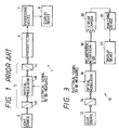
- Fig. 1 shows a conventional voltage detector 1 which uses an
electrooptical amplitude modulator 4. Input light from alight source 2 is modulated by theelectrooptical amplitude modulator 4 in accordance with an electrical signal (i.e., voltage) being provided thereto. Output light from themodulator 4 is detected by aphotodetector 6. An output signal of thephotodetector 6 is subjected to necessary processing in aprocessing device 7, and then displayed on adisplay device 8. - The
electrooptical amplitude modulator 4 consists of anoptical modulator 4B which receives the electrical signal to be measured, and apolarizer 4A andanalyzer 4C disposed on the input and output side of theoptical modulator 4B, respectively. As shown in Fig. 2, theelectrooptical amplitude modulator 4 utilizes the following relationship between the input voltage V and the output light intensity I:
where I₀ is the input light intensity and Vπ is the half-wave voltage of theelectrooptical amplitude modulator 4. Further, it is assumed that attenuation due to light absorption does not occur in themodulator 4. - If a high-speed photodetector, such as a streak camera, is employed as the
photodetector 6, a high-speed voltage detector can be constructed. - In the above-described voltage detector 1, since the output light intensity I is not proportional to the voltage V being applied, the output signal of the
photodetector 6 should be subjected to a conversion process based on equation (1) in theprocessing device 7 to obtain a signal properly representing the input voltage. - Where the input voltage is small, the resulting output light intensity from the
electrooptical amplitude modulator 4 is also small, preventing accurate voltage measurements. Further, there is a problem that noise in the light intensity of thelight source 2 deteriorates the S/N ratio of the output signal. - According to this invention a voltage detector comprising:
light source means for emitting polarized light;
modulating means for changing a polarization state of the polarized light in accordance with a voltage applied to it; and,
detecting means for determining the voltage being applied to the modulating means;
is characterised by polarization interferometer means, coupled to the modulating means, for producing an interference fringe; and by the detecting means determining the voltage at least based on movement distance of the interference fringe formed on an input surface of the detecting means. - According to the voltage detector having the above construction, the movement distance of the interference fringe is proportional to the input voltage. Therefore, precise measurements can be made without the need of performing a conversion process to obtain an output signal properly representing the input voltage. Even a smaller input voltage can easily be measured. Even where light intensity noise occurs in the light source means, it does not cause movement of the interference fringe and, therefore, the S/N ratio of the output signal is not deteriorated.
- Particular embodiments of voltage detectors in accordance with this invention will now be described with reference to the accompanying drawings; in which:-
- Fig. 1 is a block diagram showing a conventional voltage detector;
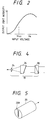
- Fig. 2 is a graph showing a relationship between a voltage applied to an electrooptical amplitude modulator and intensity of output light therefrom;
- Fig. 3 is a block diagram showing a high-speed voltage detector according to a first embodiment of the present invention;
- Fig. 4 is a block diagram showing an example of a polarization interferometer used in the first embodiment;
- Fig. 5 is a perspective view showing how an interference fringe is formed on an entrance slit of a streak camera;
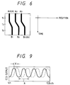
- Fig. 6 shows an example of an output image of the streak camera;
- Fig. 7 is a block diagram showing a voltage detector according to a second embodiment of the invention;
- Fig. 8 is a block diagram showing a high voltage detector according to a third embodiment of the invention;
- Fig. 9 shows an output of a one-dimensional CCD line sensor used in the third embodiment of Fig. 8;
- Fig. 10 is a block diagram showing a small-sized voltage detector according to a fourth embodiment of the invention;
- Fig. 11 is a perspective view showing a waveguide-type phase modulator used in the fourth embodiment of Fig. 10; and
- Fig. 12 shows how an interference fringe formed on an input surface of a semiconductor position-sensitive detector moves as an input voltage increases, in the fourth embodiment.
- A first embodiment of the invention is directed to a high-speed voltage detector utilizing a streak camera. As shown in Fig. 3, a high-
speed voltage detector 10 consists of alight source 12,polarizer 14,optical modulator 16 having an electrooptic crystal to which an electrical signal (i.e., voltage) to be measured is applied,polarization interferometer 18,streak camera 20 for receiving output light from thepolarization interferometer 18, analyzingdevice 22 for analyzing an output signal of thestreak camera 20, anddisplay device 23. These components are arranged in the above order from thelight source 12. The electrical signal is measured based on a movement distance of an interference fringe which is formed on the input surface of thestreak camera 20 and moves in accordance with a variation of the electrical signal being applied to theoptical modulator 16. Thepolarizer 14 may be omitted if thelight source 12 emits polarized light. - As shown in Fig. 4, the
polarization interferometer 18 consists of anobjective lens 24,birefringent crystal 26 andanalyzer 28, which are arranged in this order. Theanalyzer 28 is so arranged that its polarizing direction forms an angle of 45° with the optic axis of thebirefringent crystal 26. - As shown in Fig. 5, the
streak camera 20 is so arranged that itsentrance slit 20A traverses bands of the interference fringe. The analyzingdevice 22 determines the input voltage V based on equation (2) (described below) using intervals A between peaks of the interference fringe and a movement distance X of the peaks, which are obtained from an output image of thestreak camera 20. - The operation of the
voltage detector 10 according to the first embodiment is described next. - Upon entrance into the
polarization interferometer 18, the polarized light is expanded by theobjective lens 24, and then input to thebirefringent crystal 26. In thebirefringent crystal 26, the input light beam is split into two beams which have different polarization states in a direction determined by the optic axis of thecrystal 26 and in a direction perpendicular thereto, and which travel along different paths. As a result, the two beams having an optical path difference are output from thepolarization interferometer 18. Since, as described above, theanalyzer 28 is so arranged that its polarizing direction forms an angle of 45° with the optic axis of thebirefringent crystal 26, the two beams output from thebirefringent crystal 26 and having orthogonal polarization states interfere with each other after passing through theanalyzer 28, and the resulting interference fringe is formed on the input surface of thestreak camera 20, i.e., theentrance slit 20A. - On the other hand, the
optical modulator 16 changes the polarization state of the light in accordance with the electrical signal being applied, and provides the resulting light to thepolarization interferometer 18. Therefore, the interference fringe, which is formed on the input surface of thestreak camera 20 by thepolarization interferometer 18, moves in proportion to the polarization state variation caused by theoptical modulator 16, i.e., in proportion to the input voltage variation. - The movement distance X of the interference fringe is given by:

where A represents an interval of the interference fringe, V the voltage being applied to theoptical modulator 16, and Vπ the half-wave voltage. - Fig. 6 shows an example of an output image of the
streak camera 20 when a step-function-like electrical signal is applied. When no voltage is applied to the optical modulator 16 (at time T1), peak positions (channels) of the output image, which has been caused by the interference fringe, appear as indicated by A1-A3 in Fig. 6. In the image of Fig. 6, the vertical axis corresponds to time, and the horizontal axis to a position on theentrance slit 20A. The analyzingdevice 22 determines the channels A1-A3 of the three peaks to obtain the interval A of the interference fringe. - When an electrical signal of a certain level is applied to the
optical modulator 16 at time T2, the interference fringe is moved. Then, channels B1-B3 of the peaks in the output image of thestreak camera 20, which has been caused by the interference fringe, are determined. A movement distance X of the interference fringe is determined by comparing the channels B1-B3 with the channels A1-A3. - The voltage V is finally determined based on the movement distance X and interval A of the interference fringe and the known value Vπ in the manner as described above. A waveform of the input electrical signal is obtained by performing this calculation over the entire period in the analyzing
device 22. - It is noted that the
streak camera 20 can measure the input electrical signal in the form of not only a repetitive phenomenon but also a single phenomenon. Further, although the interference fringe is detected by thestreak camera 20 in the above embodiment, the invention is not limited to this configuration. Other one-dimensional or two-dimensional high-speed phonodetectors may be used instead of thestreak camera 20, to constitute a high-speed voltage detector. - Further, the angle formed by the polarizing direction of the
analyzer 28 and the optic axis of thebirefringent crystal 26 is not limited to 45°, but may be any angle as long as they are not parallel with or perpendicular to each other. - Next, a voltage detector according to a second embodiment of the invention is described.
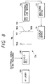
- As shown in Fig. 7, a
voltage detector 110 of the second embodiment includes alight source 12,polarizer 14,optical modulator 16 for modulating input light in accordance with an electrical signal being applied, Young'sinterferometer 116 havingpolarizer elements analyzer 118,photodetector 120, analyzingdevice 22 for analyzing an output signal of thephotodetector 120, anddisplay device 24 for displaying analysis results of the analyzingdevice 22. The above components are arranged in the above order from thelight source 12. - Young's
interferometer 116 consists of asingle slit 116A and adouble slit 117. Two slits of thedouble slit 117 extend in parallel with thesingle slit 116A, and are equipped withrespective polarizer elements - The
polarizer 14 and theanalyzer 118 are so arranged that their polarizing directions are identical or perpendicular to each other. Thepolarizing elements double slit 117 are so arranged that their polarizing directions form angles of + 45° and - 45° with the polarizing direction of thepolarizer 14, respectively. - The
photodetector 120 is either a one-dimensional photodetector or two-dimensional photodetector. Examples of the one-dimensional photodetector are a photodiode array, one-dimensional CCD line sensor and one-dimensional semiconductor position-sensitive detector. A CCD camera, two-dimensional semiconductor position-sensitive detector and image pickup tube are used as the two-dimensional photodetector. Further, a high-speed voltage detector can be constructed by using a streak camera as thephotodetector 120, as in the case of the first embodiment. - The analyzing
device 22 detects a movement distance of an interference fringe from a light and shade pattern of the interference fringe, i.e., an output pattern of thephotodetector 120. - The operation of the
voltage detector 110 of the second embodiment is described below. - Polarized light from the
polarizer 14 passes through theoptical modulator 16, Young'sinterferometer 116 andanalyzer 118, so that an interference fringe is formed on the input surface of thephotodetector 120. When an electrical signal (i.e., voltage) is applied to theoptical modulator 14, the polarization state of the output light of theoptical modulator 14 is changed in accordance with the electrical signal being applied and the interference fringe formed on the input surface of thephotodetector 120 is moved accordingly. - An interval A of bands of the interference fringe is given by:

where λ represents a wavelength of light emitted from thelight source 12, L a distance between thedouble slit 117 and thephotodetector 120, and 2d an interval between the two slits of thedouble slit 117. Further, a movement distance X of the interference fringe is moved in proportion to the voltage V being applied to theoptical modulator 14, and is expressed as:
which has the same expression as equation (2) described above. The voltage can be obtained by determining the movement distance X based on equations (3) and (4) in the analyzingdevice 22. - In the following, a high voltage detector according to a third embodiment is described.
- As shown in Fig. 8, a
high voltage detector 124 includes an argon laser 126 (acting as thelight source 12 of Fig. 7), a Pockels cell 128 (optical modulator 16) using a bulk crystal and having a half-wave voltage Vπ of 2 kV, Young'sinterferometer 116 in which film-type polarizers double slit 117, a film-type analyzer 132 (analyzer 118), and a one-dimensional CCD line sensor 134 (photodetector 120). - Fig. 9 shows an example of an output of the one-dimensional
CCD line sensor 134. The analyzingdevice 22 detects peak positions of the output of the one-dimensionalCCD line sensor 134. In the case of Fig. 9, four peak positions are detected, and their intervals A are determined. The determination of a plurality of intervals A contributes to improvement of the measurement accuracy. - When a voltage is applied to the
Pockels cell 128, the interference fringe moves to produce an output as indicated by the dashed line in Fig. 9. The analyzingdevice 22 determines the movement distances X of the respective peak positions of the interference fringe. The input voltage is determined based on equation (4) using the above-obtained peak interval A and movement distance X, and displayed on thedisplay device 24. - A small-sized voltage detector according to a fourth embodiment is described next.
- As shown in Fig. 10, a small-
sized voltage detector 136 of the fourth embodiment includes a semiconductor laser diode 138 (hereinafter referred to as "LD", and acting as thelight source 12 of Fig. 7), a waveguide-type phase modulator 140 (optical modulator 16) having Vπ of 10 V, and a semiconductor position-sensitive detector 142 (photodetector 120). - As shown in Fig. 11, the waveguide-
type phase modulator 140 has a structure in which a titanium-diffusedlight waveguide 140B is formed on a substrate of alithium niobate crystal 140A and a pair ofelectrodes waveguide 140B. In the waveguide-type phase modulator 140 of this embodiment, the distance between theelectrodes - The face-to-face coupling is provided between the
LD 138 and the titanium-diffusedlight waveguide 140B so that laser light from the former is input to the latter. Further, they are so arranged that the polarization direction of the output light from theLD 138 forms an angle of 45° with the z-axis of the crystal constituting the titanium-diffusedlight waveguide 140B. - It is noted that the
single slit 116A of Fig. 7 is not used in the fourth embodiment because the output light from the titanium-diffusedlight waveguide 140B can be regarded as polarized light emitted from a point light source. - Further, in the fourth embodiment, a film-
type analyzer 132 is employed as in the case of the third embodiment (Fig. 8), and is directly adhered to the input surface of the semiconductor position-sensitive detector 142. The semiconductor position-sensitive detector 142 is arranged so as to detect the interference fringe formed on the input surface over a length not more than one pitch thereof, i.e., to detect only one peak of the interference fringe which corresponds to the center of gravity of the interference fringe. The voltage to be measured is applied between the pair ofelectrodes type phase modulator 140. When the voltage is applied between theelectrodes waveguide 140B is subjected to phase modulation in accordance with the voltage being applied. Therefore, in the same manner as in the above embodiments, the interference fringe formed on the input surface of the semiconductor position-sensitive detector 142 is moved in accordance with the variation of the input voltage. - If an adjustment has been made such that the output of the semiconductor position-
sensitive detector 142 is zero when no voltage is applied to the waveguide-type phase modulator 140, the output itself of the semiconductor position-sensitive detector 142 becomes proportional to the voltage being applied. This means that the analyzing device can be eliminated, that is, a signal indicating the input voltage can be provided directly from the semiconductor position-sensitive detector 142 to thedisplay device 24. - Although the optical modulator of the fourth embodiment (Figs. 10 and 11) has a small half-wave voltage of 10 V, a voltage larger than the half-wave voltage 10 V can be detected by the
voltage detector 136 according to equation (1). This is explained as follows. As the input voltage to the waveguide-type phase modulator 140 increases, the interference fringe formed on the input surface of the semiconductor position-sensitive detector 142 moves accordingly as shown in Fig. 12. Since there is no upper limit on the input voltage, the movement distance of the interference fringe does not have an upper limit either. - In the fourth embodiment of Fig. 10, the movement distance of the interference fringe can be measured precisely by examining the movement distance of more than one pitch by the analyzing
device 22. - Similarly, in the second and third embodiments of Figs. 7 and 8, a movement distance of the interference fringe can be measured correctly by analyzing the movement distance of more than one pitch by the analyzing
device 22. - In the above embodiments, if the
light source 12 has a broad spectrum, a wavelength selection element such as an interference filter may be disposed immediately after the light source to obtain a narrower spectrum. This improves the visibility of the interference fringe, and contributes to production of outputs having a higher S/N ratio. - In the second to fourth embodiments, the polarizing directions of the two polarizer elements attached to the
double slit 117 are not limited to orthogonal ones, but may form any angle except that they are identical to each other.
Claims (10)
- A voltage detector comprising:
light source means (12,14,126,138) for emitting polarized light;
modulating means (16,128,140) for changing a polarization state of the polarized light in accordance with a voltage applied to it; and,
detecting means (20,120,134,142) for determining the voltage being applied to the modulating means;
characterised by polarization interferometer means (18,116,136), coupled to the modulating means (16,128,140), for producing an interference fringe; and by the detecting means (20,120,134,142) determining the voltage at least based on movement distance of the interference fringe formed on an input surface of the detecting means (20,120,134,142). - A voltage detector according to claim 1, wherein the detecting means (20,120,134,142) determines the voltage further based on a pitch of the interference fringe.
- A voltage detector according to claim 1 or 2, wherein the polarization interferometer means (18) comprises a birefringent crystal (26) to which the voltage is applied, and an analyzer (28) disposed downstream of the birefringent crystal (26).
- A voltage detector according to claim 1 or 2, wherein the polarization interferometer means (116,136) comprises a Young's interferometer which includes a single slit (116A) and a douhle slit (117) which has two slits arranged in parallel with the single slit (116A) and polarizer elements (117A,117B,130A,130B) attached to the two respective slits and having orthogonal polarizing directions, and an analyzer (118,132) disposed downstream of said Young's interferometer.
- A voltage detector according to claim 4, wherein the analyzer (118,132) is so arranged that its polarizing direction forms angles of + 45° and - 45° with the polarizing directions of the polarizer elements (117A,117B,130A,130B) of the double slit.
- A voltage detector according to any one of the preceding claims, wherein the detecting means comprises a streak camera (20).
- A voltage detector according to any one of claims 1-5, wherein the detecting means comprises a one-dimensional (134) or two dimensional photodetector.
- A voltage detector according to any one of claims 1 to 5, wherein the detecting means comprises a position-sensitive detector, and detects only one peak of the interference fringe, the one peak representing a centre of gravity of the interference fringe.
- A voltage detector according to any one of the preceding claims, wherein the modulating means (16,140) comprises an electrooptical modulator.
- A voltage detector according to claim 9, wherein the modulating means comprises a waveguide-type phase modulator (140).
Applications Claiming Priority (4)
| Application Number | Priority Date | Filing Date | Title |
|---|---|---|---|
| JP86245/91 | 1991-03-26 | ||
| JP3086245A JP2742474B2 (en) | 1991-03-26 | 1991-03-26 | High-speed voltage measurement device |
| JP3106843A JP2760668B2 (en) | 1991-04-11 | 1991-04-11 | Voltage detector |
| JP106843/91 | 1991-04-11 |
Publications (3)
| Publication Number | Publication Date |
|---|---|
| EP0506357A2 true EP0506357A2 (en) | 1992-09-30 |
| EP0506357A3 EP0506357A3 (en) | 1992-12-09 |
| EP0506357B1 EP0506357B1 (en) | 1995-12-13 |
Family
ID=26427404
Family Applications (1)
| Application Number | Title | Priority Date | Filing Date |
|---|---|---|---|
| EP92302557A Expired - Lifetime EP0506357B1 (en) | 1991-03-26 | 1992-03-25 | Optical voltage detector |
Country Status (3)
| Country | Link |
|---|---|
| US (1) | US5420686A (en) |
| EP (1) | EP0506357B1 (en) |
| DE (1) | DE69206654T2 (en) |
Families Citing this family (5)
| Publication number | Priority date | Publication date | Assignee | Title |
|---|---|---|---|---|
| DE19720246C2 (en) * | 1997-05-15 | 1999-04-15 | Deutsche Telekom Ag | Tunable interferometer |
| JP2000065531A (en) | 1998-08-26 | 2000-03-03 | Minolta Co Ltd | Interference image input device using birefringent plate |
| US6122415A (en) * | 1998-09-30 | 2000-09-19 | Blake; James N. | In-line electro-optic voltage sensor |
| JP6192890B2 (en) * | 2011-11-25 | 2017-09-06 | 東芝三菱電機産業システム株式会社 | Surface potential distribution measuring apparatus and surface potential distribution measuring method |
| CN104204720B (en) * | 2012-03-21 | 2017-03-01 | 韩国标准科学研究院 | Transparency carrier monitoring device and transparency carrier monitoring method |
Citations (2)
| Publication number | Priority date | Publication date | Assignee | Title |
|---|---|---|---|---|
| EP0299427A2 (en) * | 1987-07-13 | 1989-01-18 | Hamamatsu Photonics K.K. | Voltage detector |
| US5041779A (en) * | 1990-08-17 | 1991-08-20 | The United States Of America As Represented By The Secretary Of The Army | Nonintrusive electro-optic field sensor |
Family Cites Families (5)
| Publication number | Priority date | Publication date | Assignee | Title |
|---|---|---|---|---|
| US4232333A (en) * | 1979-01-05 | 1980-11-04 | Hamamatsu Terebi Kabushiki Kaisha | Streak image analyzing device |
| EP0197196A1 (en) * | 1985-03-08 | 1986-10-15 | The University Of Rochester | Electro-electron optical oscilloscope system for time-resolving picosecond electrical waveforms |
| FR2595820B1 (en) * | 1986-03-13 | 1990-01-05 | Bertin & Cie | OPTICAL FIBER DEVICE FOR THE REMOTE DETECTION OF A PHYSICAL QUANTITY, PARTICULARLY TEMPERATURE |
| FR2643145A1 (en) * | 1989-02-14 | 1990-08-17 | Bertin & Cie | METHOD AND DEVICE FOR DETECTING AND MEASURING A PHYSICAL SIZE |
| CH681570A5 (en) * | 1989-09-15 | 1993-04-15 | Suisse Electronique Microtech |
-
1992
- 1992-03-25 EP EP92302557A patent/EP0506357B1/en not_active Expired - Lifetime
- 1992-03-25 DE DE69206654T patent/DE69206654T2/en not_active Expired - Fee Related
-
1994
- 1994-02-22 US US08/200,568 patent/US5420686A/en not_active Expired - Fee Related
Patent Citations (2)
| Publication number | Priority date | Publication date | Assignee | Title |
|---|---|---|---|---|
| EP0299427A2 (en) * | 1987-07-13 | 1989-01-18 | Hamamatsu Photonics K.K. | Voltage detector |
| US5041779A (en) * | 1990-08-17 | 1991-08-20 | The United States Of America As Represented By The Secretary Of The Army | Nonintrusive electro-optic field sensor |
Also Published As
| Publication number | Publication date |
|---|---|
| EP0506357B1 (en) | 1995-12-13 |
| US5420686A (en) | 1995-05-30 |
| DE69206654T2 (en) | 1996-07-11 |
| DE69206654D1 (en) | 1996-01-25 |
| EP0506357A3 (en) | 1992-12-09 |
Similar Documents
| Publication | Publication Date | Title |
|---|---|---|
| EP0146244A2 (en) | Optical instrument for measuring displacement | |
| JPH0815435A (en) | Displacement-information measuring device | |
| JPH06102295A (en) | Non-contact type probe and non-contact voltage measuring device | |
| US6462539B2 (en) | Magnetic sensor with faraday element | |
| US5754282A (en) | Optical device detecting displacement information using a device for frequency-shifting an incident beam and a system for reducing beam diameter in an application direction | |
| US5774218A (en) | Laser Doppler velocimeter with electro-optical crystal | |
| US5629793A (en) | Frequency shifter and optical displacement measurement apparatus using the same | |
| US5517022A (en) | Apparatus for measuring an ambient isotropic parameter applied to a highly birefringent sensing fiber using interference pattern detection | |
| EP0506357B1 (en) | Optical voltage detector | |
| EP0294816B1 (en) | Voltage detecting device | |
| US6034761A (en) | Displacement information measuring apparatus | |
| EP0506358B1 (en) | Sampling-type optical voltage detector | |
| EP0299427B1 (en) | Voltage detector | |
| EP0199137A1 (en) | Method of and apparatus for optically measuring displacement | |
| EP0294815B1 (en) | Voltage detecting device | |
| JP2001324525A (en) | Electric field sensor | |
| JPH08146066A (en) | Electrical signal-measuring method and device | |
| JP2760668B2 (en) | Voltage detector | |
| RU2676835C1 (en) | Optical radiation mixer with application of prisms of optical active materials | |
| JPS59166873A (en) | Optical applied voltage and electric field sensor | |
| JP2742474B2 (en) | High-speed voltage measurement device | |
| JP2004012468A (en) | Electric field sensor | |
| JP4316991B2 (en) | Refractive index measuring device and concentration measuring device | |
| JPH08159867A (en) | Light-waveform measuring apparatus | |
| JP2568561B2 (en) | Optical interferometer |
Legal Events
| Date | Code | Title | Description |
|---|---|---|---|
| PUAI | Public reference made under article 153(3) epc to a published international application that has entered the european phase |
Free format text: ORIGINAL CODE: 0009012 |
|
| AK | Designated contracting states |
Kind code of ref document: A2 Designated state(s): DE FR GB |
|
| PUAL | Search report despatched |
Free format text: ORIGINAL CODE: 0009013 |
|
| AK | Designated contracting states |
Kind code of ref document: A3 Designated state(s): DE FR GB |
|
| 17P | Request for examination filed |
Effective date: 19930319 |
|
| 17Q | First examination report despatched |
Effective date: 19940921 |
|
| GRAA | (expected) grant |
Free format text: ORIGINAL CODE: 0009210 |
|
| AK | Designated contracting states |
Kind code of ref document: B1 Designated state(s): DE FR GB |
|
| REF | Corresponds to: |
Ref document number: 69206654 Country of ref document: DE Date of ref document: 19960125 |
|
| ET | Fr: translation filed | ||
| PLBE | No opposition filed within time limit |
Free format text: ORIGINAL CODE: 0009261 |
|
| STAA | Information on the status of an ep patent application or granted ep patent |
Free format text: STATUS: NO OPPOSITION FILED WITHIN TIME LIMIT |
|
| 26N | No opposition filed | ||
| PGFP | Annual fee paid to national office [announced via postgrant information from national office to epo] |
Ref country code: FR Payment date: 20010313 Year of fee payment: 10 |
|
| PGFP | Annual fee paid to national office [announced via postgrant information from national office to epo] |
Ref country code: DE Payment date: 20010319 Year of fee payment: 10 |
|
| PGFP | Annual fee paid to national office [announced via postgrant information from national office to epo] |
Ref country code: GB Payment date: 20010321 Year of fee payment: 10 |
|
| REG | Reference to a national code |
Ref country code: GB Ref legal event code: IF02 |
|
| PG25 | Lapsed in a contracting state [announced via postgrant information from national office to epo] |
Ref country code: GB Free format text: LAPSE BECAUSE OF NON-PAYMENT OF DUE FEES Effective date: 20020325 |
|
| PG25 | Lapsed in a contracting state [announced via postgrant information from national office to epo] |
Ref country code: DE Free format text: LAPSE BECAUSE OF NON-PAYMENT OF DUE FEES Effective date: 20021001 |
|
| GBPC | Gb: european patent ceased through non-payment of renewal fee |
Effective date: 20020325 |
|
| PG25 | Lapsed in a contracting state [announced via postgrant information from national office to epo] |
Ref country code: FR Free format text: LAPSE BECAUSE OF NON-PAYMENT OF DUE FEES Effective date: 20021129 |
|
| REG | Reference to a national code |
Ref country code: FR Ref legal event code: ST |