EP0504063B1 - Transceiver for the simultaneous bidirectional baseband transmission of data - Google Patents
Transceiver for the simultaneous bidirectional baseband transmission of data Download PDFInfo
- Publication number
- EP0504063B1 EP0504063B1 EP92400662A EP92400662A EP0504063B1 EP 0504063 B1 EP0504063 B1 EP 0504063B1 EP 92400662 A EP92400662 A EP 92400662A EP 92400662 A EP92400662 A EP 92400662A EP 0504063 B1 EP0504063 B1 EP 0504063B1
- Authority
- EP
- European Patent Office
- Prior art keywords
- impedance
- transmission
- generator
- transceiver
- signals
- Prior art date
- Legal status (The legal status is an assumption and is not a legal conclusion. Google has not performed a legal analysis and makes no representation as to the accuracy of the status listed.)
- Expired - Lifetime
Links
Images


Classifications
-
- H—ELECTRICITY
- H04—ELECTRIC COMMUNICATION TECHNIQUE
- H04B—TRANSMISSION
- H04B1/00—Details of transmission systems, not covered by a single one of groups H04B3/00 - H04B13/00; Details of transmission systems not characterised by the medium used for transmission
- H04B1/38—Transceivers, i.e. devices in which transmitter and receiver form a structural unit and in which at least one part is used for functions of transmitting and receiving
- H04B1/40—Circuits
- H04B1/54—Circuits using the same frequency for two directions of communication
- H04B1/58—Hybrid arrangements, i.e. arrangements for transition from single-path two-direction transmission to single-direction transmission on each of two paths or vice versa
-
- H—ELECTRICITY
- H03—ELECTRONIC CIRCUITRY
- H03K—PULSE TECHNIQUE
- H03K5/00—Manipulating of pulses not covered by one of the other main groups of this subclass
- H03K5/01—Shaping pulses
- H03K5/02—Shaping pulses by amplifying
- H03K5/026—Shaping pulses by amplifying with a bidirectional operation
-
- H—ELECTRICITY
- H04—ELECTRIC COMMUNICATION TECHNIQUE
- H04L—TRANSMISSION OF DIGITAL INFORMATION, e.g. TELEGRAPHIC COMMUNICATION
- H04L5/00—Arrangements affording multiple use of the transmission path
- H04L5/14—Two-way operation using the same type of signal, i.e. duplex
- H04L5/1423—Two-way operation using the same type of signal, i.e. duplex for simultaneous baseband signals
Definitions
- the invention relates to the transmission of digital data between stations or units via bidirectional serial links of point-to-point type.
- These links include a transmission medium, such as twisted pairs, coaxial cables or optical fibers, connected at each end to a station by a transmitter and a receiver associated with the station.
- this solution will be suitable for achieving interconnection between the units of a central computer subsystem comprising a large number of units. Indeed, the current trend being to considerably increase the number of processors and memories, the choice of a bus to carry out the exchange of information between all these units is no longer suitable. It is preferable in this context to use serial links connecting each unit to all the other units of the system so as to increase parallelism. Given the large number of links involved in such a system, the choice of bidirectional links is preferable.
- a bidirectional transmission requires at each station the presence of a transceiver connected to the lines by an adaptation impedance. It is also necessary to provide in the receiving part means making it possible to deal with collisions, that is to say the cases where the transmitters of the two interconnected stations transmit simultaneously on the common link. These means must make it possible in all circumstances to detect from the electrical state of the line the existence and nature of the signals transmitted by the remote station.
- the document EP-A-0220 626 describes a transceiver for bidirectional transmission link, provided with an adaptation impedance R11.
- the transceiver includes a differential amplifier (R2, R3, T1, T2, T4, R6) to differentiate between a signal SGN1, representative of the signal present on the link, and a signal SEN1, representative of the control signal d DATA SIGNAL 1 broadcast.
- the invention proposes another solution which does not consist in subtracting the transmission signal from the line signal when the transmitter of the station considered transmits but at contrary to adding, when the station does not transmit, the line signal to a compensation signal of the same polarity suitably chosen so that the resulting sum is representative of the transmission signal of the other station.
- the invention also relates to a simple and effective embodiment where the transceiver is further characterized in that said detection means comprise a second impedance of which a first terminal is connected to a point common to the adaptation impedance and to the line, the second terminal of which, called reception terminal, is supplied with current by a second generator controlled in response to the signals of emission control and of the same polarity as said first generator, in that said first and second generators are controlled in response to said control signals so that the first generator is active while the second generator is not and conversely, and in that said measurement signal is the voltage present on said reception terminal, said compensation value being the voltage across said second impedance, said generators and said second impedance being dimensioned so as to satisfy said compensation condition .
- said detection means comprise a second impedance of which a first terminal is connected to a point common to the adaptation impedance and to the line, the second terminal of which, called reception terminal, is supplied with current by a second generator controlled in response to the signals of emission control and of the same polarity as
- the transceiver is characterized in that said first generator comprises an adjustable current source and controlled by first servo means such that said compensation condition is satisfied.
- the solution consisting in using a external adaptation impedance to the integrated circuit causes difficulties due in particular to parasitic inductances introduced by the connections between the impedance and the terminals of the integrated circuit.
- This problem can be solved if the adaptation impedance is itself integrated, but we find the previous problems due to manufacturing dispersions and drifting characteristics.
- the transceiver is characterized in that it is part of an integrated circuit and in that the first impedance is adjustable and controlled by second means d servo such that said first impedance takes a value equal to that of a calibrated impedance outside the integrated circuit and having the value of the characteristic line impedance.
- the invention also relates to a differential type transceiver intended to be connected to a differential link formed by two lines used to convey in normal operation complementary voltages representative of a corresponding binary logic value.
- This embodiment has the advantages in particular of reducing noise and simplifying the receiver by the use of self-referenced comparators.
- the invention also relates to a transceiver characterized in that, said link comprising two transmission lines, said amplification means comprise two channels formed by two bidirectional amplifiers associated respectively with said transmission lines, in that said amplifiers are respectively controlled by two differential emission signals forming said signals transmission control, in that one of the differential signals controls the first current generator of the first amplifier as well as the second current generator of the second amplifier, the other of said differential signals controls the first generator of the second amplifier as well as the second generator of the first amplifier and in that said reception signals are a function of the differential voltage present between the reception terminals of the two bidirectional amplifiers.
- the invention also relates to an integrated circuit incorporating a plurality of transceivers having the characteristics mentioned above.
- certain elements such as the servo means may be common to several transceivers of the same integrated circuit.
- the invention finally relates to a computer system in which the interconnection between the functional units of this system is carried out by means of integrated circuits according to the invention and associated respectively with the units of this system.
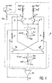
- Figure 1 is a simplified functional representation of the bidirectional amplifier used in the transceiver.
- Amplifier 1 includes an adaptation impedance R connected to line L by terminals B as well as a first current generator G1 controlled by a transmission control signal e.
- the generator G1 is connected in parallel with a circuit comprising a second impedance r connected in series with a second current generator G2 of the same polarity as the generator G1 and controlled by the signal e * complement of e.
- the terminal V of the impedance r which is connected to the current generator G2 constitutes the reception terminal whose voltage is representative of the signal emitted by the other station connected to the other end of the line L.
- the other terminal U of the impedance r is connected to the point common to the impedance R, to the generator G1 and to the line L.
- the other terminal of the impedance R is connected to a fixed potential Vdd assumed to be the ground of the circuit. In the case where the line is a coaxial cable, as shown, the cable shield is connected to ground.
- the first current generator G1 consists of a first current source S1 supplying a current I of variable intensity as a function of an adjustment signal AI.
- the current source S1 is connected to the impedance R by means of a switch T1 controlled by the signal e.
- the second generator G2 comprises a second current source S2 supplying a current i adjusted as a function of a reference voltage Vref and connected to the impedance r via a second switch T2 controlled by the signal e *.
- the current sources S1, S2 are supplied by a second fixed potential Vss negative with respect to ground.
- the impedance R is assumed to be variable as a function of adjustment signals AR by means of a decoder 8.
- the compensation condition could be satisfied by appropriate dimensioning of the resistors and current sources of the transceiver.
- means must be provided which make it possible to automatically adjust the characteristics of the components and circuits so as to compensate for manufacturing dispersions and characteristic drifts.
- FIG. 2 This figure represents an integrated circuit comprising several transceivers of which only the bidirectional amplifiers 1 are shown. Each amplifier 1 is connected to an associated line L via the pads B of the integrated circuit.
- the circuit includes means for controlling the currents I and the adaptation impedances R of the amplifiers 1.
- the control of I is carried out by means of a current control circuit 2 connected to a control impedance Ra of constitution and dimensioning as a function of the impedances R.
- the circuit 2 provides a current adjustment signal AI applied to the adjustment input of the current sources S1 of the amplifiers 1.
- the circuit 2 is designed so as to adjust the current I of the sources of current to check the compensation condition mentioned above.
- the detailed description of circuit 2 will be given in relation to FIG. 4.
- the impedance servo means R comprise a resistance control circuit 3 connected to the servo impedance Ra and to a calibrated impedance Rc external to the integrated circuit.
- Circuit 3 provides a control signal AR for the servo impedance Ra and the impedances R of the amplifiers.
- Circuit 3 controls the value of the resistances Ra and R to the value of the calibrated resistance Rc equal to the characteristic impedance of the lines L. Circuit 3 will be described in detail with reference to FIG. 6.
- the means for controlling the intensity I and the impedances R ensure that the compensation condition will be verified whatever the manufacturing dispersions and the drift in characteristics while maintaining the condition of adaptation of the adaptation impedances.
- FIG. 3 represents an embodiment in BiCMOS technology of a bidirectional amplifier of the differential type. It is functionally equivalent to two bidirectional amplifiers in accordance with FIG. 1, arranged symmetrically and connected respectively to the lines L, L * of a differential link. As in differential mode only one of the channels is active at a time, it suffices to provide a single current source S1, S2 common to the current generators G1, G2, associated with the two channels.
- the left channel associated with line L comprises an adaptation impedance R connected by point U to line L and to the collector of a bipolar transistor T1 whose emitter is connected to the first common current source S1 .
- the base of transistor T1 receives the emission control signal e.
- the collector of transistor T1 is connected to the collector V of a second transistor T2 via the impedance r.
- the emitter of transistor T2 is connected to the second common current source S2.
- the right channel connected to the second line L * of the differential link comprises an adaptation impedance R connected by the point U * to the collector of a transistor T1 * whose emitter is connected to the common current source S1.
- the collector of transistor T1 * is connected to the collector V * of transistor T2 * via the impedance r.
- the emitter of transistor T2 * is connected to the second common current source S2.
- the transistor T1 * receives on its base the signal e * complement of the signal e.
- the signals e and e * constitute differential transmission control signals. These signals are complementary and representative of a determined logic value.
- the signals e and e * are applied respectively on the basis of the transistors T2 * and T2, via resistors serving to compensate for the time constant due to the structural capacity of the impedances R.
- the current source S1 consists of a bipolar transistor T3 whose collector is connected to the emitters of the transistors T1 and T1 * and whose emitter is connected to the negative potential Vss via the drain-source path of an NMOS transistor N1.
- the base of transistor T3 is controlled by the adjustment signal AI and the gate of transistor N1 receives the power supply control signal AUTO.
- the second current source S2 consists of a bipolar transistor T4 whose collector is connected to the emitters of transistors T2 and T2 * and whose emitter is connected to the voltage Vss via a resistor N2.
- the operation of the circuit of FIG. 3 is easily deduced from that of FIG. 1 thanks to the following remarks.
- the first current generator G1 consists of the transistor T1 or T1 * acting as a switch and the first common current source S1.
- the second current generator G2 is formed by the transistor T2 or T2 * and the second current source S2.
- Each channel then operates exactly like the circuit of FIG. 1 but, taking into account the differential operating mode, only one of the transmission control signals e, e * is active at a time, as well for the transceiver of the station considered only for that of the remote station.
- the voltages present at the measurement terminals V and V * will respectively take the values - RI and -RI / 2 or - RI / 2 and - RI depending on whether the left channel or the right channel of the remote station transmitter is active or not.
- the voltages V and V * therefore constitute a differential signal which is a function of the differential transmit signal of the remote station and can be used downstream of the amplifier after appropriate shaping.
- FIG. 4 represents a current control circuit 2 particularly suitable for controlling the differential amplifier of FIG. 3.
- the compensation condition requires that the voltage drop in the resistors R and r in series must be the same when the transmitter in question is the only one to transmit and when no transmitter is transmitting. Consequently, the circuit of FIG. 4 is designed so as to simulate these two cases, to compare the corresponding measurement voltages and to adjust the current I so as to obtain the equality of these voltages.
- the circuit of FIG. 4 includes a control circuit 9 of the same constitution and same dimensioning for the most part as the differential amplifier of FIG. 3 but modified so as to carry out the desired simulations on its two channels.
- a fixed differential emission control signal is applied to the bases of the transistors T1, T1 * so as to make them respectively conductive and non-conductive.
- the emitter of transistor T1 * is connected to its base while the base of transistor T1 receives a positive voltage with respect to Vss.
- This voltage is supplied by an assembly comprising a bipolar transistor T5 whose base and collector are connected to ground and whose emitter is connected to the potential Vss by an appropriate resistor.
- the emitter of transistor T5 supplies the base voltage of transistor T1.
- the adaptation impedance R and the second impedance r are replaced respectively by a servo impedance Ra, Ra * and an impedance z.
- the choice of the values of Ra, Ra * and z must take into account the fact that, unlike circuit 9, the transceiver has its adaptation impedances R connected to the lines and that consequently the current source S1 supplies an impedance equivalent equal to half the adaptation impedance.
- the servo impedances Ra, Ra * could be produced by placing in parallel two impedances identical to the adaptation impedances R used in the transceiver. In this case, the impedance z would be identical to r.
- servo impedances Ra, Ra * identical to the adaptation impedance R, by choosing for z a value equal to twice that of the second impedance r.
- the impedance r will then be achieved by putting two impedances identical to z in parallel.
- This solution simplifies the realization of the servo impedances Ra, Ra * which, like the adaptation impedances R, are preferably adjustable.
- this solution allows the impedance Ra of the left channel to be used to control the impedances R, as we will see below.
- the impedances R and Ra on the one hand, r and z on the other hand have the same value but the current supplied by the current source S1 of the servo circuit 9 is half of that supplied by the source S1 of the bidirectional amplifier. For this, it is sufficient to size the transistor N1 of the circuit 9 so that it has a resistance twice that of the amplifier. Insofar as R is not negligible with respect to r, Ra * should be equal to R / 2.
- the voltages V and V * are proportional to the voltage drops across the impedances R and r of the transmitter respectively when it is the only one to transmit and when no transmitter transmits.
- the voltages V and V * are applied respectively to the direct and inverting input of a differential amplifier 10 with high gain and high input impedance, the output of which provides the current adjustment signal AI which is then applied to the base of the transistors T3 of current sources S1 of the servo circuit 9 and bidirectional amplifiers 1.
- the amplifier 10 could be replaced by a digital circuit analogous to that used for the enslavement of the impedances as we will see in detail later.
- circuit of FIG. 4 regulates the current I of the current sources S1 so as to permanently maintain the desired compensation condition.
- control circuit 9 Since the control circuit 9 is essentially of the same constitution and dimensioning as the bidirectional amplifiers 1, it reproduces with good precision their behavior independently of the manufacturing dispersions and takes account of the possibly leakage currents of the switching transistors T1 , T1 *, T2, T2 *.
- this circuit ensures that the compensation condition will be strictly verified from the static point of view, which is generally sufficient since the characteristic line impedance, therefore the impedances R and r, are, for high frequencies, practically pure resistances.
- the impedances R and r are, for high frequencies, practically pure resistances.
- the latter comprise a second identical current source S2 formed by the transistor T4 in series with a resistor N2. It follows that the voltage Vref applied to the base of the transistor T4 fixes the voltage drop in the resistor N2 and consequently the current i which flows through it. Thus, taking into account the dimensioning condition imposed by the servo circuit, the choice of the voltage Vref indirectly determines the RI product which must be fixed precisely because it fixes the dynamics of the signals.
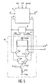
- FIG. 5 represents the reception part as a whole.
- the circuit 5 receives the voltages V, V * from the amplifier 1 and provides a differential signal VAL, VAL * resulting from the comparison between the differential voltage V, V * and a determined threshold value.
- the circuit 5 is in fact made up of a set of comparators for respectively comparing the voltages V and V * at a threshold value between the maximum and minimum voltages that can be taken by V and V * when the remote station is active. If one of the voltages V or V * is greater than this threshold in absolute value, a logic circuit places the outputs VAL and VAL * of circuit 5 respectively at a high and low level. Otherwise, the signals VAL and VAL * are placed respectively at low and high levels.
- the realization of circuit 5 being within the reach of the skilled person, we will not give a more detailed description.
- the shaping circuit 4 is an AND gate in ECL technology composed of two transistors T6, T7 linked together by their transmitter and whose collectors are each connected to ground via a resistor.
- Two other transistors T8, T9 have their emitter connected to the collector of a fifth transistor T10, the emitter of which is connected to the voltage Vss via a resistor N3.
- the collector of transistor T8 is connected to the emitters of transistors T6 and T7 while the collector of transistor T9 is connected to the collector of transistor T7.
- the base of transistor T10 receives the reference voltage Vref so as to fix the current flowing in the resistor N3.
- the bases of the transistors T6 and T7 respectively receive the voltages V * and V.
- the bases of the transistors T8 and T9 receive the line activity signals VAL and VAL * respectively.
- the voltages s * and s of the collectors of the transistors T6 and T7 constitute the differential reception signals usable downstream in the rest of the circuit.
- the circuit of Figure 5 operates as follows. If the remote station is active, there is a differential voltage V, V * which is detected by the circuit 5 then providing a positive differential signal VAL, VAL *. As a result, the transistor T8 is conductive and the transistor T9 is blocked. Circuit 4 works then as a differential amplifier producing on its outputs s, s * a differential signal as a function of the differential voltage V, V *.
- the circuit 5 detects the inactivity of the remote station, the signals VAL and VAL * take values complementary to the previous case. The transistor T8 is then blocked and the transistor T9 is conductive. As a result, the signal s is in the low state and the signal s * is in the high state, thus forcing the differential output of the shaping circuit to the logic value 0.
- FIG. 6 represents the means for controlling the adaptation impedances R. They include an impedance comparator 3 connected to a reference impedance Rc and to a control impedance Ra.
- the reference impedance Rc is a calibrated impedance external to the integrated circuit and the impedance Ra is an integrated impedance adjustable with the same constitution and dimensioning as the adaptation impedances R to be adjusted.
- the impedance comparator 3 delivers a digital adjustment signal AR connected to the decoders 7, 8 associated respectively with the impedance Ra and with each adaptation impedance R.
- Each decoder 7, 8 controls the value of the associated impedance.
- the decoders 8 associated with the adaptation impedances R differ from the decoder 7 of the impedance Ra by the presence of an additional input INF * provided for the test operations which will be explained later.
- the embodiment described below allows the part to be adjusted purely resistive adaptation impedances. Those skilled in the art can modify this embodiment to take into account, if necessary, the real characteristics of the line.
- the impedance comparator 3 comprises two voltage dividing bridges Pa, Pc connected in parallel with Ra and Rc respectively. These two parallel assemblies are supplied respectively by identical current sources Sa and Sc.
- the source Sa is in fact the source S1 of the circuit 9.
- the comparator 3 also includes a voltage comparator 11 connected to the dividing bridges Pa and Pc as well as an up-down counter 6.
- the voltage comparator 11 is in fact made up of two comparators CL, CH supplying respectively an INC increment signal applied to the counting input of the up-down counter 6 and a decrement signal DEC applied to its countdown input.
- the midpoint c of the divider bridge Pc of resistance 2X is connected to the inverting input of the comparator CL and to the direct input of the comparator CH.
- the divider bridge Pa has two intermediate terminals a, b such that the resistance X between the point a and the ground and the resistance between the point b and the current source Sa are equal, a resistance x between the points a and b being equal at a fraction of X.
- Point a is connected to the inverting input of comparator CH and point b is connected to the direct input of comparator CL.
- This arrangement makes it possible, by appropriate dimensioning of X and x, to produce a hysteresis effect such that the INC increment or DEC decrement signals are active when the value of the servo impedance Ra is respectively less than or greater than the value of the reference impedance Rc of a determined threshold value.
- This has the advantage of avoiding instability in the regulation of the adaptation impedances.
- This threshold value will be defined by a percentage of error imposed and relating to the value of Rc.
- the operation of the comparator 3 is practically independent of the manufacturing dispersions, insofar as X is sufficiently large with respect to Rc, which is always possible.
- the state of the up-down counter 6 is representative of the setting value to be applied to the impedances R and Ra so that their value is equal to the value of the reference impedance Rc to within an error percentage.
- the slaving of FIG. 6 is therefore of the numerically controlled type.
- this solution has the disadvantage that the analog adjustment signal is exposed to alterations during its transmission in the circuit, in particular in the case of an integrated circuit comprising a large number of transceivers.
- each variable impedance is produced by means of a plurality of resistors selectively connected in parallel by a digital adjustment signal.
- the impedance Ra is slightly different from that of the impedances R because it is not necessary to provide for the possibility for Ra to take an infinite value for the test operations. Consequently, one of the resistors of Ra can be permanently connected.
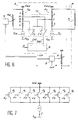
- FIG. 7 represents such an embodiment where each resistor consists of a PMOS transistor P0-P6.
- the transistors are connected in parallel, their sources being connected to ground and their drains to the associated current source.
- the gates of the transistors P0-P6 are controlled respectively by the signals E0-E6.
- the resistance of the drain-source path of each transistor then takes a value which depends on the dimensioning of the transistor (its gate width for example) as well as the manufacturing process, with an uncertainty around a typical value corresponding to the most likely case. .
- the solution chosen consists in using a coded digital adjustment signal as the AR adjustment signal and in associating with each impedance to adjust a corresponding decoder 7, 8.
- the code used is advantageously a Gray code supplied directly by the up-down counter 6. A detailed embodiment of this up-down counter and the associated decoders is shown in FIG. 8.
- the characteristic line impedance being 50 ohms, for example an error of less than 5% is imposed on the adaptation impedances, within the limits of a dispersion of about 25% on the values of the components.
- the adaptation impedances must then be able to vary regularly between 37 and 63 ohms approximately in the typical case.
- the calculations and simulations then lead to a solution with 7 transistors PO to P6 of increasing resistances, the dimensions of which are easy to calculate according to the technology used.
- the INC increment or DEC decrement signals must be activated when the impedance Ra is respectively lower or higher by 5% than the impedance Rc.
- R.I. 0.5 V, this results in noise immunity for a noise level below 3.3 mV.
- FIG. 8 represents the up-down counter 6 and the decoders 7 and 8 in the particular case where the adaptation impedances comprise 7 PMOS transistors in parallel.
- the decoder 7 associated with Ra has only 6 outputs C1 to C6 connected respectively to the gates of the transistors P1 to P6.
- the transistor P0 is permanently made conductive by a negative bias of its gate.
- a output C1-C6 of decoder 7 takes the logic value 0, the transistor which it controls P1-P6 is made conductive.
- the decoder 8 has 7 outputs E0 to E6 and operates similar to the decoder 7 with the difference that the first transistor P0 can be conductive or blocked depending on whether the output E0 is at 0 or at 1.
- the up-down counter 6 comprises three flip-flops DA, DB, DC of type D defining the state of the counter.
- the flip-flops DA, DB, DC receive respectively on their inputs D the logic signals A + , B + , C + supplied by a set of logic gates as a function of the signals INC and DEC and of the states A, B, C of the flip-flops DA, DB, DC.
- the counter can take seven different states, state 000 being prohibited.
- Each state A, B, C corresponds to the value coded in Gray code of the number of transistors which must be in the conducting state. This provision implies that any modification imposed on the value of the impedances to be regulated results in the change of state of only one of the flip-flops DA, DB, DC at the same time.
- the flip-flops are synchronized by the falling edges of a clock signal Ho as a function of a primary signal H and of the state of an additional flip-flop DH.
- the flip-flop DH receives on its reverse clock input CK * the clock signal H and on its input D the logical sum DEC + INC.
- the clock signal H and the non-inverting output Q of the flip-flop DH are connected to the inputs of a NAND gate (NAND) GH delivering the signal Ho to the reverse clock inputs CK * of the flip-flops DA, DB, DC.
- NAND NAND gate
- the up-down counter 6 operates as follows. When the difference in absolute value between the values of Ra and Rc is less than the threshold, the signals DEC and INC remain at 0. During a falling edge of the clock signal H, the flip-flop DH is set to 0 and the output Ho of the gate GH is maintained at 1, which prohibits any change of state of the flip-flops DA, DB, DC. If, on the other hand, the difference between Ra and Rc exceeds the threshold, one of the signals DEC or INC is at 1 and the input D of the flip-flop DH receives the logical value 1. When the following falling clock edge appears, the state of the flip-flop DH reverts to 1 and the output of the gate GH delivers a signal complementary to the clock signal H. The output of the gate GH is therefore at 1 but returns to 0 on the appearance of the next rising edge of H and the flip-flops DA, DB, DC are updated in accordance with equations (1), (2), (3) above.
- the up-down counter is only activated when a modification has to take place and this makes it possible to simplify the logic circuit for controlling the flip-flops.
- the flip-flop DH and the gate GH the flip-flops DA, DB, DC are perfectly synchronized by the clock H without risk of disturbance by the appearance of the signals INC or DEC.
- the decoders 7 and 8 receive the state signals A, B, C from the flip-flops DA, DB, DC or their complement and supply as output the signals C1-C6 or E0-E6 controlling the associated variable impedances.
- FIG. 9 represents a parallel-series, series-parallel interface circuit in which the invention can be applied advantageously.
- This circuit is assumed to be produced in the form of an integrated circuit intended to be connected on the one hand to parallel input-output lines composed of data lines DT and control lines CT and on the other hand to transmission lines L series.
- the circuit comprises serialization-deserialization means 14 connected to the parallel input-output DT, CT as well as to the various transceivers 12 by associated serial transmission and reception lines.
- Each transceiver 12 is connected to a bidirectional transmission line L via an amplifier 1 in accordance with the preceding description.
- Each line L connects the transceiver associated with another transceiver belonging to a remote station.
- the integrated circuit also comprises the means 2, 3 for controlling the current I and the adaptation impedances R of the amplifiers.
- a clock generator 13 receiving a master clock signal CL supplied by an external clock controls the serialization-deserialization means 14.
- the generator 13 operates at a frequency multiplier so as to adapt the transmission rate serial data at the parallel data reception rate.
- the generator 13 regenerates a clock signal at the frequency of the serial data from this data and performs a frequency division to control the parallel part of the serializer-deserializer.
- circuits 13 and 14 are the subject of an example of embodiment detailed in each of the following French patent applications filed on 11.07.90: "Process and system for digital serial data transmission", No. 90.08811; “Data serialization and deserialization device and resulting serial digital data transmission system", n ° 90.08812; “Data sampling device and resulting digital data transmission system”, No. 90.08813.
- the circuit 14 further comprises means for selecting the transceivers and supplying them with the signals INF and AUTO with a view to respectively carrying out the test operations and the power supply failure of the amplifiers associated with the inactive lines.
- the serialization-deserialization means 14 include circuits for controlling the activity of the transceivers as a function of CT commands indicating the destination station. Conversely, these circuits are designed to deliver control signals on the parallel interface in response to the identity of the lines active in reception.
- decoding circuits supplying the signals INF and AUTO to the transceivers designated by appropriate CT commands. The practical implementation of these circuits essentially depends on the parallel interface chosen. For example, if the CT commands have an address part and a control part, the address part will be used as input to address decoders. Test command signals and power control signals from the control part will be used to validate one of the INF or AUTO signals selected by the address decoder.
- Figures 10, 11 and 12 symbolize the test operations that can be performed on the integrated circuit of Figure 9.
- the serializer-deserializer 14 of the integrated circuit 16 is connected by its parallel inputs-outputs to a test device 15.
- the circuit 14 is connected to the transceivers 12, only one of which is shown for reasons of clarity.
- the integrated circuit 16 is tested after manufacture, before being connected to the serial transmission lines.
- the tester 15 controls the setting of the signal INF of the transceiver to be tested to 0, which results in its current source supplies the adaptation impedances in their normal configuration.
- the tester 15 controls the transmission by this transceiver of a set of data applied to the parallel inputs of the circuit 14.
- the circuit 14 converts them into serial data and transmits them to the selected transceiver 12.
- the amplifier 1 of the transceiver 12 receives transmission control signals which consequently activate the current sources supplying the adaptation impedances.
- the source S1 supplies only the adaptation impedance R of the active channel, therefore outputs on an impedance double the equivalent impedance which it supplies when the transceiver is in operation normal. Consequently, the voltage V or V * of the active channel takes the value - RI On the other hand, the voltage V * or V of the inactive channel takes the value - (R + r) i, that is to say practically say - RI / 2.
- the voltages V and V * which appear on the reception terminals of the amplifier 1 therefore reproduce the transmission control signals which, after shaping and conversion into parallel data, are received by the test apparatus 15. This the latter then performs the comparison between the parallel data originally transmitted and that received. If there is a coincidence, this means that circuits 13, 14 and 12 have worked correctly.
- the test operations of the integrated circuit are very simple and make it possible to verify not only the proper functioning of the transceivers but also of all additional and intermediate circuits such as the serializer-deserializer 14.
- Tests can also be carried out while the integrated circuit is in place in a system, its transceivers being connected to the transmission lines L.
- the test apparatus 15 controls the setting to 1 of the signal INF of the transceiver to be tested, which forces its adaptation impedances to the infinite value.
- the current source of its amplifier 1 supplies only the transmission lines L.
- the adaptation impedances have a value equal to the characteristic impedance of the lines, we find our in the same situation as in FIG. 10 and the test can be done in the same way.
- the test gives an additional indication of the integrity of the connections between the transceiver and the terminals of the integrated circuit and of the connections between the terminals and the lines.
- the transceivers of two integrated circuits 16, 16 ′ are linked together by the lines L and the test apparatus controls the setting of the signal INF of the transceiver to 0 of the integrated circuit to be tested 16 and setting the INF signal of the corresponding transceiver of the other integrated circuit 16 'to 1.
- the transceiver 12 of circuit 16 is in its normal configuration, while that of circuit 16 'has its adaptation impedances disconnected.
- the line L is open at its end which is connected to the circuit 16 'and consequently, the signals emitted by the circuit 16 are transmitted by the line to the circuit 16', are reflected there then retransmitted by the line to the circuit 16. It follows that the reflection of the signals simulates an emission from the circuit 16 ′ and a transmission by a line of length twice that of the real line, with the possibility of collisions between the signals transmitted and the signals received.
- test can therefore be carried out as previously but it will provide an additional indication of the integrity of the line and of the connections between the line and the transceiver of the remote station. In addition, this test takes into account any current losses during the transmission. Finally, the reflection effect can be exploited to locate line faults by analyzing the reception signals and the delay between transmission and reception of the test signals.
- test according to FIG. 12 reveals a fault
- test according to FIG. 11 will indicate whether the fault is due to circuit 16 or not.
- test methods are particularly advantageous in the case of a high-speed link since only low frequency signals are exchanged between the test and the integrated circuit to be tested.
- test circuits controlled from the outside, capable of automatically generating test signals. parallel, perform the comparisons and store the results of these comparisons in registers accessible from the outside.
- This test circuit will include a test signal generator, for example a random signal generator, controlled by an activation circuit which will be programmed to trigger the sending of a determined number of test words.
- a test signal generator for example a random signal generator
- the comparison circuits must be designed to take account of the offsets between the signals sent and the signals received. This can be done by means of buffer memories.
- a less bulky embodiment consists in associating with the comparison circuits a generator of test signals identical to that of transmission, programmed in the same way and synchronized by the reception clock. This embodiment makes it possible to delete the buffers as well as the resynchronization circuits which would be necessary otherwise.
- test circuits inside the integrated circuit has the double advantage of not requiring an external test device and of allowing much better exhaustiveness of the tests. Indeed, the use of a test device would considerably slow down test operations because of the desynchronization between transmission and reception, which involves numerous operations of writing and reading in the memory of the device. test.
- test signal generators Comparison and storage means are within the reach of those skilled in the art and therefore does not require a more detailed description.
Abstract
Description
L'invention concerne les transmissions de données numériques entre stations ou unités par l'intermédiaire de liaisons série bidirectionnelles de type point à point. Ces liaisons comportent un support de transmission, tel que paires torsadées, câbles coaxiaux ou fibres optiques, relié à chaque extrémité à une station par un émetteur et un récepteur associé à la station.The invention relates to the transmission of digital data between stations or units via bidirectional serial links of point-to-point type. These links include a transmission medium, such as twisted pairs, coaxial cables or optical fibers, connected at each end to a station by a transmitter and a receiver associated with the station.
Pour de nombreuses applications, on préfère utiliser un mode de transmission permettant un fonctionnement simultané dans les deux sens entre les deux points afin d'obtenir une meilleure utilisation des lignes.For many applications, it is preferred to use a transmission mode allowing simultaneous operation in both directions between the two points in order to obtain better use of the lines.
En particulier, cette solution sera adaptée pour réaliser l'interconnexion entre les unités d'un sous-système central informatique comportant un grand nombre d'unités. En effet, la tendance actuelle étant d'augmenter considérablement le nombre de processeurs et de mémoires, le choix d'un bus pour effectuer les échanges d'informations entre toutes ces unités n'est plus adapté. Il est préférable dans ce contexte d'utiliser des liaisons série reliant chaque unité à toutes les autres unités du système de façon à augmenter le parallélisme. Compte tenu du grand nombre de liaisons impliquées dans un tel système, le choix de liaisons bidirectionnelles est préférable.In particular, this solution will be suitable for achieving interconnection between the units of a central computer subsystem comprising a large number of units. Indeed, the current trend being to considerably increase the number of processors and memories, the choice of a bus to carry out the exchange of information between all these units is no longer suitable. It is preferable in this context to use serial links connecting each unit to all the other units of the system so as to increase parallelism. Given the large number of links involved in such a system, the choice of bidirectional links is preferable.
De façon générale, une transmission bidirectionnelle nécessite au niveau de chaque station la présence d'un émetteur-récepteur relié aux lignes par une impédance d'adaptation. Il faut en outre prévoir dans la partie réceptrice des moyens permettant de traiter les collisions, c'est-à-dire les cas où les émetteurs des deux stations reliées entre elles émettent simultanément sur la liaison commune. Ces moyens doivent permettre en toute circonstance de détecter à partir de l'état électrique de la ligne l'existence et la nature des signaux émis par la station éloignée.In general, a bidirectional transmission requires at each station the presence of a transceiver connected to the lines by an adaptation impedance. It is also necessary to provide in the receiving part means making it possible to deal with collisions, that is to say the cases where the transmitters of the two interconnected stations transmit simultaneously on the common link. These means must make it possible in all circumstances to detect from the electrical state of the line the existence and nature of the signals transmitted by the remote station.
Pour résoudre ce problème, on utilise habituellement le principe d'une compensation dans le récepteur de l'effet produit sur la ligne par l'émetteur de la même station lorsque celui-ci émet. Ceci revient à effectuer en cas d'émission une soustraction du signal d'émission au signal présent sur la ligne. La différence obtenue est alors représentative du signal émis par l'émetteur de la station éloignée. Une telle solution est décrite dans la demande de brevet européen EP-A-186 142 intitulée "Two wire bidirectional digital transmission system".To solve this problem, we usually use the principle of compensation in the receiver for the effect produced on the line by the transmitter of the same station when it transmits. This amounts to performing a subtraction of the transmission signal from the signal on the line in the event of transmission. The difference obtained is then representative of the signal transmitted by the transmitter of the remote station. Such a solution is described in European patent application EP-A-186 142 entitled "Two wire bidirectional digital transmission system".
Le document EP-A-0220 626 décrit un émetteur-récepteur pour liaison de transmission bidirectionnelle, muni d'une impédance d'adaptation R11. L'émetteur-récepteur comprend un amplificateur différentiel (R2, R3, T1, T2, T4, R6) pour effectuer la différence entre un signal SGN1, représentatif du signal présent sur la liaison, et un signal SEN1, représentatif du signal de commande d'émission DATA SIGNAL 1.The document EP-A-0220 626 describes a transceiver for bidirectional transmission link, provided with an adaptation impedance R11. The transceiver includes a differential amplifier (R2, R3, T1, T2, T4, R6) to differentiate between a signal SGN1, representative of the signal present on the link, and a signal SEN1, representative of the control signal
Le document US-A-3909 559 décrit un émetteur-récepteur pour liaison de transmission bidirectionnelle à deux conducteurs dont l'un est mis à la masse. Selon les figures 3 et 4 de ce document, il semblerait possible de connecter plusieurs émetteurs-récepteurs identiques sur une même liaison à condition de brancher au moins une impédance d'adaptation entre les deux conducteurs, à l'extérieur des émetteurs-récepteurs.Document US-A-3909 559 describes a transceiver for two-way two-way transmission link, one of which is grounded. According to FIGS. 3 and 4 of this document, it would seem possible to connect several identical transceivers on the same link provided that at least one adaptation impedance is connected between the two conductors, outside the transceivers.
L'invention propose une autre solution consistant non pas à soustraire du signal de ligne le signal d'émission lorsque l'émetteur de la station considérée émet mais au contraire à additionner, lorsque la station n'émet pas, le signal de ligne à un signal de compensation de même polarité convenablement choisi pour que la somme en résultant soit représentative du signal d'émission de l'autre station.The invention proposes another solution which does not consist in subtracting the transmission signal from the line signal when the transmitter of the station considered transmits but at contrary to adding, when the station does not transmit, the line signal to a compensation signal of the same polarity suitably chosen so that the resulting sum is representative of the transmission signal of the other station.
Plus précisément l'invention a pour objet un émetteur-récepteur prévu pour être relié par une liaison de transmission à un autre émetteur-récepteur analogue, ladite liaison comportant au moins une ligne de transmission, ledit émetteur-récepteur comportant des moyens d'amplification pour produire des signaux d'émission sur ladite liaison en réponse à des signaux de commande d'émission et pour produire des signaux de réception en réponse aux signaux d'émission produits sur ladite liaison par l'autre émetteur-récepteur, ledit émetteur-récepteur étant caractérisé en ce que lesdits moyens d'amplification comportent pour chaque ligne de transmission un amplificateur bidirectionnel 1 comprenant:
- une première impédance d'adaptation à la ligne et connectée à celle-ci,
- un premier générateur commandé en réponse auxdits signaux de commande d'émission et alimentant en parallèle ladite première impédance et ladite ligne,
- des moyens de détection, commandés en réponse auxdits signaux de commande d'émission, pour fournir un signal de mesure qui est représentatif soit du courant circulant dans l'impédance d'adaptation lorsque ledit premier générateur est actif, soit de la somme du courant circulant dans l'impédance d'adaptation et d'une valeur de compensation lorsque ledit premier générateur n'est pas actif,
- a first impedance for adapting to the line and connected to it,
- a first generator controlled in response to said transmission control signals and supplying said first impedance and said line in parallel,
- detection means, controlled in response to said emission control signals, to supply a measurement signal which is representative either of the current flowing in the adaptation impedance when said first generator is active, or of the sum of the current flowing in the adaptation impedance and a compensation value when said first generator is not active,
De multiples réalisations sont envisageables pour produire un signal représentatif de la somme de deux courants. Néanmoins, l'invention présente l'avantage qu'elle permet de choisir des réalisations particulièrement simples car les circuits pour additionner deux signaux de même polarité peuvent être plus simples que ceux qui effectuent les différences.Multiple embodiments are possible to produce a signal representative of the sum of two currents. However, the invention has the advantage that it makes it possible to choose particularly simple embodiments because the circuits for adding two signals of the same polarity can be simpler than those which make the differences.
Cet avantage est particulièrement appréciable si l'on cherche à obtenir un fonctionnement à très haute fréquence car la complexité des circuits entraîne toujours des perturbations dues notamment aux liaisons électriques et aux connexions.This advantage is particularly appreciable if one seeks to obtain a very high frequency operation because the complexity of the circuits always leads to disturbances due in particular to the electrical connections and the connections.
Aussi, l'invention concerne également une réalisation simple et efficace où l'émetteur-récepteur est en outre caractérisé en ce que lesdits moyens de détection comportent une seconde impédance dont une première borne est reliée à un point commun à l'impédance d'adaptation et à la ligne, dont la seconde borne, appelée borne de réception, est alimentée en courant par un second générateur commandé en réponse aux signaux de commande d'émission et de même polarité que ledit premier générateur, en ce que lesdits premier et second générateurs sont commandés en réponse auxdits signaux de commande de façon à ce que le premier générateur soit actif alors que le second générateur ne l'est pas et réciproquement, et en ce que ledit signal de mesure est la tension présente sur ladite borne de réception, ladite valeur de compensation étant la tension aux bornes de ladite seconde impédance, lesdits générateurs et ladite seconde impédance étant dimensionnés de façon à satisfaire ladite condition de compensation.Also, the invention also relates to a simple and effective embodiment where the transceiver is further characterized in that said detection means comprise a second impedance of which a first terminal is connected to a point common to the adaptation impedance and to the line, the second terminal of which, called reception terminal, is supplied with current by a second generator controlled in response to the signals of emission control and of the same polarity as said first generator, in that said first and second generators are controlled in response to said control signals so that the first generator is active while the second generator is not and conversely, and in that said measurement signal is the voltage present on said reception terminal, said compensation value being the voltage across said second impedance, said generators and said second impedance being dimensioned so as to satisfy said compensation condition .
La condition de compensation mentionnée ci-dessus impose, comme nous le verrons en détail ultérieurement, une relation entre les valeurs des impédances et des courants impliqués dans l'amplificateur bidirectionnel. Dans le cas d'une réalisation au moyen de circuits discrets, il serait possible de vérifier cette relation par un simple dimensionnement des composants de l'amplificateur bidirectionnel. Par contre, cette solution est difficilement applicable dans le cas d'un circuit intégré à cause des dispersions de fabrication ainsi que des dérives des caractéristiques par vieillissement ou variations de température.The compensation condition mentioned above imposes, as we will see in detail later, a relationship between the values of the impedances and of the currents involved in the bidirectional amplifier. In the case of an embodiment by means of discrete circuits, it would be possible to verify this relation by a simple dimensioning of the components of the bidirectional amplifier. On the other hand, this solution is difficult to apply in the case of an integrated circuit because of manufacturing dispersions as well as drifts in the characteristics by aging or variations in temperature.
Pour résoudre ce problème, et selon une caractéristique particulière de l'invention, l'émetteur-récepteur est caractérisé en ce que ledit premier générateur comporte une source de courant réglable et commandée par des premiers moyens d'asservissement tels que ladite condition de compensation soit satisfaite.To solve this problem, and according to a particular characteristic of the invention, the transceiver is characterized in that said first generator comprises an adjustable current source and controlled by first servo means such that said compensation condition is satisfied.
D'autre part, pour réaliser un émetteur-récepteur intégré capable de fonctionner à haut débit, par exemple de l'ordre de 1 Gbit/s, la solution consistant à utiliser une impédance d'adaptation externe au circuit intégré entraîne des difficultés dues notamment aux inductances parasites introduites par les connexions entre l'impédance et les bornes du circuit intégré. Ce problème peut être résolu si l'impédance d'adaptation est elle-même intégrée mais on retrouve les problèmes précédents dûs aux dispersions de fabrication et aux dérives des caractéristiques.On the other hand, to achieve an integrated transceiver capable of operating at high speed, for example of the order of 1 Gbit / s, the solution consisting in using a external adaptation impedance to the integrated circuit causes difficulties due in particular to parasitic inductances introduced by the connections between the impedance and the terminals of the integrated circuit. This problem can be solved if the adaptation impedance is itself integrated, but we find the previous problems due to manufacturing dispersions and drifting characteristics.
Pour résoudre ce dernier problème et selon un autre aspect de l'invention, l'émetteur-récepteur est caractérisé en ce qu'il fait partie d'un circuit intégré et en ce que la première impédance est réglable et commandée par des seconds moyens d'asservissement tels que ladite première impédance prenne une valeur égale à celle d'une impédance calibrée extérieure au circuit intégré et ayant la valeur de l'impédance caractéristique de la ligne.To solve this latter problem and according to another aspect of the invention, the transceiver is characterized in that it is part of an integrated circuit and in that the first impedance is adjustable and controlled by second means d servo such that said first impedance takes a value equal to that of a calibrated impedance outside the integrated circuit and having the value of the characteristic line impedance.
D'autres caractéristiques de l'émetteur-récepteur selon l'invention apparaîtront dans la suite de la description.Other characteristics of the transceiver according to the invention will appear in the following description.
En particulier, l'invention concerne également un émetteur-récepteur de type différentiel destiné à être relié à une liaison différentielle formée de deux lignes servant à véhiculer en fonctionnement normal des tensions complémentaires représentatives d'une valeur logique binaire correspondante. Cette réalisation présente les avantages notamment de diminuer le bruit et de simplifier le récepteur par l'utilisation de comparateurs auto-référencés.In particular, the invention also relates to a differential type transceiver intended to be connected to a differential link formed by two lines used to convey in normal operation complementary voltages representative of a corresponding binary logic value. This embodiment has the advantages in particular of reducing noise and simplifying the receiver by the use of self-referenced comparators.
Aussi, l'invention a également pour objet un émetteur-récepteur caractérisé en ce que, ladite liaison comprenant deux lignes de transmission, lesdits moyens d'amplification comportent deux voies formées de deux amplificateurs bidirectionnels associés respectivement auxdites lignes de transmission, en ce que lesdits amplificateurs sont commandés respectivement par deux signaux différentiels d'émission formant lesdits signaux de commande d'émission, en ce que l'un des signaux différentiels commande le premier générateur de courant du premier amplificateur ainsi que le second générateur de courant du second amplificateur, l'autre desdits signaux différentiels commande le premier générateur du second amplificateur ainsi que le second générateur du premier amplificateur et en ce que lesdits signaux de réception sont fonction de la tension différentielle présente entre les bornes de réception des deux amplificateurs bidirectionnels.Also, the invention also relates to a transceiver characterized in that, said link comprising two transmission lines, said amplification means comprise two channels formed by two bidirectional amplifiers associated respectively with said transmission lines, in that said amplifiers are respectively controlled by two differential emission signals forming said signals transmission control, in that one of the differential signals controls the first current generator of the first amplifier as well as the second current generator of the second amplifier, the other of said differential signals controls the first generator of the second amplifier as well as the second generator of the first amplifier and in that said reception signals are a function of the differential voltage present between the reception terminals of the two bidirectional amplifiers.
L'invention concerne également un circuit intégré incorporant une pluralité d'émetteurs-récepteurs ayant les caractéristiques mentionnées ci-dessus. Dans ce cas, certains éléments tels que les moyens d'asservissement pourront être communs à plusieurs émetteurs-récepteurs du même circuit intégré.The invention also relates to an integrated circuit incorporating a plurality of transceivers having the characteristics mentioned above. In this case, certain elements such as the servo means may be common to several transceivers of the same integrated circuit.
L'invention concerne enfin un système informatique dans lequel l'interconnexion entre les unités fonctionnelles de ce système est réalisée au moyen de circuits intégrés conformes à l'invention et associés respectivement aux unités de ce système.The invention finally relates to a computer system in which the interconnection between the functional units of this system is carried out by means of integrated circuits according to the invention and associated respectively with the units of this system.
D'autres aspects, détails de réalisation et avantages de l'émetteur-récepteur selon l'invention seront également exposés dans la description qui va suivre.
- La figure 1 représente un amplificateur bidirectionnel utilisé dans l'émetteur-récepteur selon l'invention.
- La figure 2 représente les moyens d'asservissement associés à l'amplificateur bidirectionnel.
- La figure 3 représente un amplificateur bidirectionnel de type différentiel.
- La figure 4 représente une réalisation des premiers moyens d'asservissement.
- La figure 5 représente la partie réception des moyens d'amplification de l'émetteur-récepteur selon l'invention.
- La figure 6 représente des seconds moyens d'asservissement.
- La figure 7 représente un mode de réalisation d'une impédance d'adaptation réglable.
- La figure 8 représente des circuits permettant de réaliser les seconds moyens d'asservissement.
- La figure 9 représente un circuit d'interface parallèle-série, série-parallèle utilisant l'émetteur-récepteur selon l'invention.
- Les figures 10, 11 et 12 illustrent les procédés de test applicables aux émetteurs-récepteurs et aux circuits intégrés selon l'invention.
- FIG. 1 represents a bidirectional amplifier used in the transceiver according to the invention.
- FIG. 2 represents the control means associated with the bidirectional amplifier.
- FIG. 3 represents a bidirectional amplifier of the differential type.
- Figure 4 shows an embodiment of the first control means.
- FIG. 5 represents the reception part of the amplification means of the transceiver according to the invention.
- Figure 6 shows second servo means.
- FIG. 7 represents an embodiment of an adjustable adaptation impedance.
- FIG. 8 represents circuits making it possible to produce the second control means.
- FIG. 9 represents a parallel-serial, serial-parallel interface circuit using the transceiver according to the invention.
- Figures 10, 11 and 12 illustrate the test methods applicable to transceivers and integrated circuits according to the invention.
La figure 1 est une représentation fonctionnelle simplifiée de l'amplificateur bidirectionnel utilisé dans l'émetteur-récepteur.Figure 1 is a simplified functional representation of the bidirectional amplifier used in the transceiver.
L'amplificateur 1 comprend une impédance d'adaptation R reliée à la ligne L par des bornes B ainsi qu'un premier générateur de courant G1 commandé par un signal de commande d'émission e. Le générateur G1 est branché en parallèle avec un montage comportant une seconde impédance r branchée en série avec un second générateur de courant G2 de même polarité que le générateur G1 et commandé par le signal e* complément de e. La borne V de l'impédance r qui est reliée au générateur de courant G2 constitue la borne de réception dont la tension est représentative du signal émis par l'autre station reliée à l'autre extrémité de la ligne L. L'autre borne U de l'impédance r est reliée au point commun à l'impédance R, au générateur G1 et à la ligne L. L'autre borne de l'impédance R est reliée à un potentiel fixe Vdd supposé être la masse du circuit. Dans le cas où la ligne est un câble coaxial, comme représenté, le blindage du câble est relié à la masse.
Le premier générateur de courant G1 est constitué d'une première source de courant S1 fournissant un courant I d'intensité variable en fonction d'un signal de réglage AI. La source de courant S1 est reliée à l'impédance R par l'intermédiaire d'un interrupteur T1 commandé par le signal e.The first current generator G1 consists of a first current source S1 supplying a current I of variable intensity as a function of an adjustment signal AI. The current source S1 is connected to the impedance R by means of a switch T1 controlled by the signal e.
De façon analogue, le second générateur G2 comporte une seconde source de courant S2 fournissant un courant i réglé en fonction d'une tension de référence Vref et reliée à l'impédance r par l'intermédiaire d'un second interrupteur T2 commandé par le signal e*.Similarly, the second generator G2 comprises a second current source S2 supplying a current i adjusted as a function of a reference voltage Vref and connected to the impedance r via a second switch T2 controlled by the signal e *.
Les sources de courant S1, S2 sont alimentées par un second potentiel fixe Vss négatif par rapport à la masse. L'impédance R est supposée variable en fonction de signaux de réglage AR par l'intermédiaire d'un décodeur 8.The current sources S1, S2 are supplied by a second fixed potential Vss negative with respect to ground. The impedance R is assumed to be variable as a function of adjustment signals AR by means of a
Pour simplifier les explications du principe de fonctionnement de l'amplificateur bidirectionnel, nous supposerons tout d'abord que la ligne L est sans perte, que i est négligeable par rapport à I et que la valeur de l'impédance R est très petite par rapport à celle de r. D'autre part, nous supposerons qu'un amplificateur bidirectionnel de même constitution d'une station éloignée est connecté à l'autre extrémité de la ligne L. Enfin, nous supposerons que l'état d'émission d'une station se traduit par la mise à 1 logique du signal de commande d'émission e qui, dans ce cas, provoque la fermeture de l'interrupteur T1 et l'ouverture de l'interrupteur T2.To simplify the explanations of the operating principle of the bidirectional amplifier, we will first assume that the line L is lossless, that i is negligible compared to I and that the value of the impedance R is very small compared to that of r. On the other hand, we will assume that a bi-directional amplifier of the same constitution of a distant station is connected to the other end of the line L. Finally, we will assume that the emission state of a station results in the logic setting of the emission control signal e which, in this case, causes the closing of the switch T1 and the opening of the switch T2.
En fonctionnement, quatre situations peuvent se présenter:
- a) La station considérée est seule à émettre. Le générateur G2 est alors inactif tandis que le générateur G1 fournit un courant I à l'impédance R en parallèle avec l'impédance caractéristique de la ligne L. L'impédance R étant supposée adaptée à la ligne, un courant I/2 circule dans cette impédance et la tension présente à la borne U ainsi qu'à la borne V est égale à - R.I/2.
- b) Si aucune station n'émet, le générateur G1 de chaque station est inactif, les générateurs G2 sont actifs. La tension à la borne V est alors pratiquement égale à - r.i.
- c) Si les deux stations émettent, les générateurs G2 sont inactifs et le courant I produit par le premier générateur G1 de la station et celui de la station éloignée se superposent dans les impédances R et dans la ligne. En supposant un fonctionnement linéaire, la tension présente à la borne U ainsi qu'à la borne V est donc égale à - R.I.
- d) Si la station éloignée est seule à émettre, un courant I/2 circule dans l'impédance R et la tension présente à la borne U est égale à - R.I/2. D'autre part, le courant i circule dans l'impédance r et la tension à la borne V est donc égale à - r.i - R.I/2.
- a) The station considered is the only one to transmit. The generator G2 is then inactive while the generator G1 supplies a current I at the impedance R in parallel with the characteristic impedance of the line L. The impedance R being supposed to be adapted to the line, a current I / 2 flows in this impedance and the voltage present at terminal U as well as at terminal V is equal to - RI / 2.
- b) If no station transmits, the generator G1 of each station is inactive, the generators G2 are active. The voltage at terminal V is then practically equal to - ri
- c) If the two stations transmit, the generators G2 are inactive and the current I produced by the first generator G1 of the station and that of the distant station are superimposed in the impedances R and in the line. Assuming linear operation, the voltage present at terminal U as well as at terminal V is therefore equal to - RI
- d) If the distant station is the only one to transmit, a current I / 2 flows in impedance R and the voltage present at terminal U is equal to - RI / 2. On the other hand, the current i flows in the impedance r and the voltage at the terminal V is therefore equal to - ri - RI / 2.
Le but étant d'obtenir un signal ne dépendant que de l'état d'émission de la station éloignée, on constate que si l'on choisit les valeurs des impédances r et R et des courants i et I telles que l'on ait la relation : r.i = R.I/2, la tension de la borne de réception V vérifie bien cette condition. Cette tension sera donc égale à - R.I lorsque la station éloignée émet et à -R.I/2 lorsqu'elle n'émet pas.The aim being to obtain a signal which only depends on the emission state of the remote station, it can be seen that if one chooses the values of the impedances r and R and of the currents i and I such that one has the relation: ri = RI / 2, the voltage of the reception terminal V verifies this condition well. This voltage will therefore be equal to - R.I when the remote station transmits and to -R.I / 2 when it does not transmit.
Il convient cependant de remarquer que la relation r.i = R.I/2 permet d'obtenir des niveaux de tension sur la borne V strictement indépendants de l'état d'émission de la station à condition que les hypothèses initiales soient parfaitement vérifiées. Dans le cas contraire, la tension à la borne de réception V dépendrait de l'état d'émission mais la compensation imparfaite qui en résulterait pourrait, dans certaines conditions, permettre tout de même de détecter l'émission de la station éloignée en comparant la tension de réception à des valeurs de seuil bien choisies.It should however be noted that the relation ri = RI / 2 makes it possible to obtain voltage levels on the terminal V strictly independent of the emission state of the station provided that the initial hypotheses are fully verified. Otherwise, the voltage at the reception terminal V would depend on the transmission state, but the imperfect compensation that would result from it could, under certain conditions, still make it possible to detect the transmission from the remote station by comparing the reception voltage at well chosen threshold values.
Un calcul plus précis permettrait d'établir une relation entre R, I, r, i pour réaliser exactement la compensation dans le cas réel. Cette relation doit exprimer la condition que la chute de tension dans les impédances R et r en série observée lorsque l'émetteur considéré est seul à émettre est égale à celle observée quand aucun émetteur n'émet. Cette condition est rigoureuse en fonctionnement linéaire et reste valable sans qu'il soit nécessaire de faire des hypothèses sur l'ordre de grandeur de la résistance r ou du courant i, ni sur l'impédance caractéristique de la ligne.A more precise calculation would make it possible to establish a relation between R, I, r, i to carry out exactly the compensation in the real case. This relation must express the condition that the voltage drop in the impedances R and r in series observed when the transmitter considered is the only one to transmit is equal to that observed when no transmitter transmits. This condition is rigorous in linear operation and remains valid without it being necessary to make assumptions on the order of magnitude of the resistance r or of the current i, nor on the characteristic impedance of the line.
Ainsi, en supposant un fonctionnement idéal des générateurs de courant, la condition de compensation s'exprime par la relation : R.I/2 = (R/2 + r). iThus, assuming an ideal operation of the current generators, the compensation condition is expressed by the relation: R.I / 2 = (R / 2 + r). i
La condition de compensation pourrait être satisfaite grâce à un dimensionnement approprié des résistances et des sources de courant de l'émetteur-récepteur. Cependant, dans la perspective d'une réalisation intégrée, il faut prévoir des moyens permettant d'ajuster automatiquement les caractéristiques des composants et des circuits de façon à compenser les dispersions de fabrication et les dérives de caractéristiques.The compensation condition could be satisfied by appropriate dimensioning of the resistors and current sources of the transceiver. However, from the perspective of an integrated embodiment, means must be provided which make it possible to automatically adjust the characteristics of the components and circuits so as to compensate for manufacturing dispersions and characteristic drifts.
Dans ce but, on prévoit des moyens d'asservissement représentés schématiquement à la figure 2. Cette figure représente un circuit intégré comportant plusieurs émetteurs-récepteurs dont seuls les amplificateurs bidirectionnels 1 sont représentés. Chaque amplificateur 1 est relié à une ligne associée L par l'intermédiaire des plots B du circuit intégré. Le circuit comporte des moyens d'asservissement des courants I et des impédances d'adaptation R des amplificateurs 1. L'asservissement de I est effectué au moyen d'un circuit de commande de courant 2 relié à une impédance d'asservissement Ra de constitution et de dimensionnement fonction des impédances R. Le circuit 2 fournit un signal AI de réglage de courant appliqué à l'entrée de réglage des sources de courant S1 des amplificateurs 1. Le circuit 2 est conçu de façon à régler le courant I des sources de courant pour vérifier la condition de compensation évoquée précédemment. La description détaillée du circuit 2 sera donnée en relation à la figure 4.For this purpose, provision is made for servo-control means shown diagrammatically in FIG. 2. This figure represents an integrated circuit comprising several transceivers of which only the
Les moyens d'asservissement des impédances R comportent un circuit de commande de résistance 3 relié à l'impédance d'asservissement Ra et à une impédance calibrée Rc extérieure au circuit intégré. Le circuit 3 fournit un signal de réglage AR de l'impédance d'asservissement Ra et des impédances R des amplificateurs. Le circuit 3 asservit la valeur des résistances Ra et R à la valeur de la résistance calibrée Rc égale à l'impédance caractéristique des lignes L. Le circuit 3 sera décrit en détail en référence à la figure 6.The impedance servo means R comprise a
Les moyens d'asservissement de l'intensité I et des impédances R assurent que la condition de compensation sera vérifiée quelles que soient les dispersions de fabrication et les dérives de caractéristiques tout en maintenant la condition d'adaptation des impédances d'adaptation.The means for controlling the intensity I and the impedances R ensure that the compensation condition will be verified whatever the manufacturing dispersions and the drift in characteristics while maintaining the condition of adaptation of the adaptation impedances.
La figure 3 représente une réalisation en technologie BiCMOS d'un amplificateur bidirectionnel de type différentiel. Il est fonctionnellement équivalent à deux amplificateurs bidirectionnels conformes à la figure 1, disposés symétriquement et reliés respectivement aux lignes L, L* d'une liaison différentielle. Comme en mode différentiel une seule des voies est active à la fois, il suffit de prévoir une seule source de courant S1, S2 commune aux générateurs de courant G1, G2, associés aux deux voies.FIG. 3 represents an embodiment in BiCMOS technology of a bidirectional amplifier of the differential type. It is functionally equivalent to two bidirectional amplifiers in accordance with FIG. 1, arranged symmetrically and connected respectively to the lines L, L * of a differential link. As in differential mode only one of the channels is active at a time, it suffices to provide a single current source S1, S2 common to the current generators G1, G2, associated with the two channels.
Ainsi, la voie de gauche associée à la ligne L comporte une impédance d'adaptation R reliée par le point U à la ligne L et au collecteur d'un transistor bipolaire T1 dont l'émetteur est relié à la première source de courant commune S1. La base du transistor T1 reçoit le signal de commande d'émission e. Le collecteur du transistor T1 est relié au collecteur V d'un second transistor T2 par l'intermédiaire de l'impédance r. L'émetteur du transistor T2 est relié à la seconde source de courant commune S2. Symétriquement, la voie de droite reliée à la seconde ligne L* de la liaison différentielle comporte une impédance d'adaptation R reliée par le point U* au collecteur d'un transistor T1* dont l'émetteur est relié à la source de courant commune S1. Le collecteur du transistor T1* est relié au collecteur V* du transistor T2* par l'intermédiaire de l'impédance r. L'émetteur du transistor T2* est relié à la seconde source de courant commune S2. Le transistor T1* reçoit sur sa base le signal e* complément du signal e. Les signaux e et e* constituent des signaux différentiels de commande d'émission. Ces signaux sont complémentaires et représentatifs d'une valeur logique déterminée. Les signaux e et e* sont appliqués respectivement sur la base des transistors T2* et T2, par l'intermédiaire de résistances servant à compenser la constante de temps due à la capacité de structure des impédances R.Thus, the left channel associated with line L comprises an adaptation impedance R connected by point U to line L and to the collector of a bipolar transistor T1 whose emitter is connected to the first common current source S1 . The base of transistor T1 receives the emission control signal e. The collector of transistor T1 is connected to the collector V of a second transistor T2 via the impedance r. The emitter of transistor T2 is connected to the second common current source S2. Symmetrically, the right channel connected to the second line L * of the differential link comprises an adaptation impedance R connected by the point U * to the collector of a transistor T1 * whose emitter is connected to the common current source S1. The collector of transistor T1 * is connected to the collector V * of transistor T2 * via the impedance r. The emitter of transistor T2 * is connected to the second common current source S2. The transistor T1 * receives on its base the signal e * complement of the signal e. The signals e and e * constitute differential transmission control signals. These signals are complementary and representative of a determined logic value. The signals e and e * are applied respectively on the basis of the transistors T2 * and T2, via resistors serving to compensate for the time constant due to the structural capacity of the impedances R.
La source de courant S1 est constituée d'un transistor bipolaire T3 dont le collecteur est relié aux émetteurs des transistors T1 et T1* et dont l'émetteur est relié au potentiel négatif Vss par l'intermédiaire du chemin drain-source d'un transistor NMOS N1. La base du transistor T3 est commandée par le signal de réglage AI et la grille du transistor N1 reçoit le signal de commande d'alimentation AUTO. De façon analogue, la seconde source de courant S2 est constituée d'un transistor bipolaire T4 dont le collecteur est relié aux émetteurs des transistors T2 et T2* et dont l'émetteur est relié à la tension Vss par l'intermédiaire d'une résistance N2.The current source S1 consists of a bipolar transistor T3 whose collector is connected to the emitters of the transistors T1 and T1 * and whose emitter is connected to the negative potential Vss via the drain-source path of an NMOS transistor N1. The base of transistor T3 is controlled by the adjustment signal AI and the gate of transistor N1 receives the power supply control signal AUTO. Similarly, the second current source S2 consists of a bipolar transistor T4 whose collector is connected to the emitters of transistors T2 and T2 * and whose emitter is connected to the voltage Vss via a resistor N2.
Le fonctionnement du circuit de la figure 3 se déduit facilement de celui de la figure 1 grâce aux remarques suivantes. Pour chaque voie, le premier générateur de courant G1 est constitué du transistor T1 ou T1* faisant fonction d'interrupteur et de la première source de courant commune S1. De même, le second générateur de courant G2 est formé du transistor T2 ou T2* et de la seconde source de courant S2. Chaque voie fonctionne alors exactement comme le circuit de la figure 1 mais, compte tenu du mode de fonctionnement différentiel, un seul des signaux de commande d'émission e, e* est actif à la fois, aussi bien pour l'émetteur-récepteur de la station considérée que pour celui de la station éloignée. Il en résulte que, grâce à la compensation décrite précédemment, les tensions présentes aux bornes de mesure V et V* prendront respectivement les valeurs - RI et -RI/2 ou - RI/2 et - RI selon que la voie de gauche ou la voie de droite de l'émetteur de la station éloignée est active ou non. Les tensions V et V* constituent donc un signal différentiel fonction du signal différentiel d'émission de la station éloignée et pourra être exploité en aval de l'amplificateur après une mise en forme appropriée.The operation of the circuit of FIG. 3 is easily deduced from that of FIG. 1 thanks to the following remarks. For each channel, the first current generator G1 consists of the transistor T1 or T1 * acting as a switch and the first common current source S1. Likewise, the second current generator G2 is formed by the transistor T2 or T2 * and the second current source S2. Each channel then operates exactly like the circuit of FIG. 1 but, taking into account the differential operating mode, only one of the transmission control signals e, e * is active at a time, as well for the transceiver of the station considered only for that of the remote station. It follows that, thanks to the compensation described above, the voltages present at the measurement terminals V and V * will respectively take the values - RI and -RI / 2 or - RI / 2 and - RI depending on whether the left channel or the right channel of the remote station transmitter is active or not. The voltages V and V * therefore constitute a differential signal which is a function of the differential transmit signal of the remote station and can be used downstream of the amplifier after appropriate shaping.
La figure 4 représente un circuit de commande de courant 2 particulièrement adapté pour commander l'amplificateur différentiel de la figure 3. Nous avons vu que la condition de compensation impose que la chute de tension dans les résistances R et r en série doit être la même lorsque l'émetteur considéré est seul à émettre et lorsqu'aucun émetteur n'émet. Par conséquent, le circuit de la figure 4 est conçu de façon à simuler ces deux cas, à comparer les tensions de mesure correspondantes et à régler le courant I de façon à obtenir l'égalité de ces tensions.FIG. 4 represents a
Dans ce but, le circuit de la figure 4 comporte un circuit d'asservissement 9 de même constitution et de même dimensionnement pour l'essentiel que l'amplificateur différentiel de la figure 3 mais modifié de façon à réaliser sur ses deux voies les simulations recherchées. En particulier, un signal de commande d'émission différentiel fixe est appliqué aux bases des transistors T1, T1* de façon à les rendre respectivement conducteur et non-conducteur. Pour cela, l'émetteur du transistor T1* est relié à sa base tandis que la base du transistor T1 reçoit une tension positive par rapport à Vss. Cette tension est fournie par un montage comportant un transistor bipolaire T5 dont la base et le collecteur sont reliés à la masse et dont l'émetteur est relié au potentiel Vss par une résistance appropriée. L'émetteur du transistor T5 fournit la tension de base du transistor T1.For this purpose, the circuit of FIG. 4 includes a control circuit 9 of the same constitution and same dimensioning for the most part as the differential amplifier of FIG. 3 but modified so as to carry out the desired simulations on its two channels. . In particular, a fixed differential emission control signal is applied to the bases of the transistors T1, T1 * so as to make them respectively conductive and non-conductive. For this, the emitter of transistor T1 * is connected to its base while the base of transistor T1 receives a positive voltage with respect to Vss. This voltage is supplied by an assembly comprising a bipolar transistor T5 whose base and collector are connected to ground and whose emitter is connected to the potential Vss by an appropriate resistor. The emitter of transistor T5 supplies the base voltage of transistor T1.
D'autre part, l'impédance d'adaptation R et la seconde impédance r sont remplacées respectivement par une impédance d'asservissement Ra, Ra* et une impédance z. Le choix des valeurs de Ra, Ra* et z doit tenir compte du fait que, contrairement au circuit 9, l'émetteur-récepteur a ses impédances d'adaptation R reliées aux lignes et que par conséquent la source de courant S1 alimente une impédance équivalente égale à la moitié de l'impédance d'adaptation. Ainsi, selon une première possibilité, les impédances d'asservissement Ra, Ra* pourraient être réalisées en plaçant en parallèle deux impédances identiques aux impédances d'adaptation R utilisées dans l'émetteur-récepteur. Dans ce cas, l'impédance z serait identique à r.On the other hand, the adaptation impedance R and the second impedance r are replaced respectively by a servo impedance Ra, Ra * and an impedance z. The choice of the values of Ra, Ra * and z must take into account the fact that, unlike circuit 9, the transceiver has its adaptation impedances R connected to the lines and that consequently the current source S1 supplies an impedance equivalent equal to half the adaptation impedance. Thus, according to a first possibility, the servo impedances Ra, Ra * could be produced by placing in parallel two impedances identical to the adaptation impedances R used in the transceiver. In this case, the impedance z would be identical to r.
Selon une autre possibilité, on utilise des impédances d'asservissement Ra, Ra* identiques à l'impédance d'adaptation R, en choisissant pour z une valeur égale au double de celle de la seconde impédance r. L'impédance r sera alors réalisée par la mise en parallèle de deux impédances identiques à z. Cette solution simplifie la réalisation des impédances d'asservissement Ra, Ra* qui, comme les impédances d'adaptation R, sont de préférence réglables. De plus, cette solution permet d'utiliser l'impédance Ra de la voie de gauche pour réaliser l'asservissement des impédances R, comme nous le verrons plus loin.According to another possibility, use is made of servo impedances Ra, Ra * identical to the adaptation impedance R, by choosing for z a value equal to twice that of the second impedance r. The impedance r will then be achieved by putting two impedances identical to z in parallel. This solution simplifies the realization of the servo impedances Ra, Ra * which, like the adaptation impedances R, are preferably adjustable. In addition, this solution allows the impedance Ra of the left channel to be used to control the impedances R, as we will see below.
Selon encore une autre possibilité, les impédances R et Ra d'une part, r et z d'autre part ont la même valeur mais le courant fourni par la source de courant S1 du circuit d'asservissement 9 est moitié de celui fourni par la source S1 de l'amplificateur bidirectionnel. Pour cela, il suffit de dimensionner le transistor N1 du circuit 9 pour qu'il ait une résistance double de celui de l'amplificateur. Dans la mesure où R n'est pas négligeable par rapport à r, il conviendrait que Ra* soit égale à R/2.According to yet another possibility, the impedances R and Ra on the one hand, r and z on the other hand have the same value but the current supplied by the current source S1 of the servo circuit 9 is half of that supplied by the source S1 of the bidirectional amplifier. For this, it is sufficient to size the transistor N1 of the circuit 9 so that it has a resistance twice that of the amplifier. Insofar as R is not negligible with respect to r, Ra * should be equal to R / 2.
Dans tous les cas, toujours en supposant un fonctionnement linéaire, les tensions V et V* sont proportionnelles aux chutes de tension aux bornes des impédances R et r de l'émetteur respectivement lorsqu'il est seul à émettre et lorsqu'aucun émetteur n'émet. Les tensions V et V* sont appliquées respectivement à l'entrée directe et inverseuse d'un amplificateur différentiel 10 à grand gain et forte impédance d'entrée dont la sortie fournit le signal de réglage de courant AI qui est ensuite appliqué à la base des transistors T3 des sources de courant S1 du circuit d'asservissement 9 et des amplificateurs bidirectionnels 1.In all cases, always assuming linear operation, the voltages V and V * are proportional to the voltage drops across the impedances R and r of the transmitter respectively when it is the only one to transmit and when no transmitter transmits. The voltages V and V * are applied respectively to the direct and inverting input of a
Selon une variante de réalisation, l'amplificateur 10 pourrait être remplacé par un montage numérique analogue à celui utilisé pour l'asservissement des impédances comme nous le verrons en détail ultérieurement.According to an alternative embodiment, the
De façon évidente, le circuit de la figure 4 règle le courant I des sources de courant S1 de façon à maintenir en permanence la condition de compensation recherchée.Obviously, the circuit of FIG. 4 regulates the current I of the current sources S1 so as to permanently maintain the desired compensation condition.
Le circuit d'asservissement 9 étant pour l'essentiel de même constitution et dimensionnement que les amplificateurs bidirectionnels 1, il reproduit avec une bonne précision leur comportement indépendamment des dispersions de fabrication et tient compte des courants de fuite éventuellement non négligeables des transistors de commutation T1, T1*, T2, T2*.Since the control circuit 9 is essentially of the same constitution and dimensioning as the
Bien entendu, ce circuit assure que la condition de compensation sera strictement vérifiée du point de vue statique, ce qui est suffisant en général car l'impédance caractéristique de la ligne, donc les impédances R et r, sont, pour des fréquences élevées, pratiquement des résistances pures. L'homme du métier pourra bien sûr adapter cette réalisation pour mieux tenir compte des caractéristiques réelles de la ligne dans chaque cas particulier.Of course, this circuit ensures that the compensation condition will be strictly verified from the static point of view, which is generally sufficient since the characteristic line impedance, therefore the impedances R and r, are, for high frequencies, practically pure resistances. Those skilled in the art will of course be able to adapt this embodiment to better take into account the real characteristics of the line in each particular case.
Selon un aspect intéressant de la réalisation de l'amplificateur bidirectionnel et du circuit d'asservissement, ces derniers comportent une seconde source de courant S2 identique formée du transistor T4 en série avec une résistance N2. Il en résulte que la tension Vref appliquée à la base du transistor T4 fixe la chute de tension dans la résistance N2 et par conséquent le courant i qui la traverse. Ainsi, compte tenu de la condition de dimensionnement imposée par le circuit d'asservissement, le choix de la tension Vref détermine indirectement le produit R.I qui doit être fixé avec précision car il fixe la dynamique des signaux.According to an interesting aspect of the embodiment of the bidirectional amplifier and the servo circuit, the latter comprise a second identical current source S2 formed by the transistor T4 in series with a resistor N2. It follows that the voltage Vref applied to the base of the transistor T4 fixes the voltage drop in the resistor N2 and consequently the current i which flows through it. Thus, taking into account the dimensioning condition imposed by the servo circuit, the choice of the voltage Vref indirectly determines the RI product which must be fixed precisely because it fixes the dynamics of the signals.
Dans le cadre d'une application à un circuit d'interface parallèle-série, série-parallèle pour réaliser l'interconnexion d'un grand nombre d'unités, il est intéressant de prévoir la possibilité de couper l'alimentation des circuits de puissance des émetteurs et récepteurs inactifs. C'est pourquoi les sources de courant S1 sont munies d'un transistor NMOS N1 commandé par un signal de mise sous tension AUTO. Cette disposition présente l'avantage, notamment dans le cas d'une réalisation intégrée, de réduire la consommation du circuit d'interface.In the context of an application to a parallel-series, series-parallel interface circuit for interconnecting a large number of units, it is advantageous to provide for the possibility of cutting the power supply to the power circuits inactive transmitters and receivers. This is why the current sources S1 are provided with an NMOS transistor N1 controlled by an AUTO power-up signal. This arrangement has the advantage, in particular in the case of an integrated embodiment, of reducing the consumption of the interface circuit.
Il convient cependant de tenir compte de cette possibilité dans la conception de la partie réception de l'émetteur-récepteur. En effet, si l'émetteur-récepteur de la station éloignée est à l'état de repos, c'est-à-dire a sa source de courant S1 inactive, aucune des lignes différentielles n'est alimentée par cet émetteur-récepteur. Il en résulte qu'aucune tension différentielle V, V* n'apparaît en sortie de l'amplificateur bidirectionnel, ce qui pourrait provoquer une détection erronée des signaux de réception. Pour éviter cette difficulté, il est prévu un ensemble de moyens dans la partie réception de l'émetteur-récepteur pour traiter ce cas.However, this possibility should be taken into account in the design of the reception part of the transceiver. Indeed, if the transceiver of the remote station is in the idle state, that is to say at its current source S1 inactive, none of the differential lines is supplied by this transceiver. As a result, no differential voltage V, V * appears at the output of the bidirectional amplifier, which could cause an erroneous detection of the reception signals. To avoid this difficulty, a set of means is provided in the reception part of the transceiver to deal with this case.
La figure 5 représente la partie réception dans son ensemble. On retrouve évidemment l'amplificateur bidirectionnel 1 qui est associé à un circuit de mise en forme 4 et à un circuit de détection d'activité de ligne 5. Le circuit 5 reçoit les tensions V, V* de l'amplificateur 1 et fournit un signal différentiel VAL, VAL* résultant de la comparaison entre la tension différentielle V, V* et une valeur de seuil déterminée. Le circuit 5 est constitué en fait d'un ensemble de comparateurs pour comparer respectivement les tensions V et V* à une valeur de seuil comprise entre les tensions maximales et minimales pouvant être prises par V et V* lorsque la station éloignée est active. Si l'une des tensions V ou V* est supérieure à ce seuil en valeur absolue, un circuit logique place respectivement à un niveau haut et bas les sorties VAL et VAL* du circuit 5. Dans le cas contraire, les signaux VAL et VAL* sont placés respectivement à des niveaux bas et haut. La réalisation du circuit 5 étant à la portée de l'homme du métier, nous n'en donnerons pas une description plus détaillée.FIG. 5 represents the reception part as a whole. Obviously there is the
Le circuit de mise en forme 4 est une porte ET en technologie ECL composée de deux transistors T6, T7 reliés entre eux par leur émetteur et dont les collecteurs sont reliés chacun à la masse par l'intermédiaire d'une résistance. Deux autres transistors T8, T9 ont leur émetteur relié au collecteur d'un cinquième transistor T10 dont l'émetteur est relié à la tension Vss par l'intermédiaire d'une résistance N3. Le collecteur du transistor T8 est relié aux émetteurs des transistors T6 et T7 tandis que le collecteur du transistor T9 est relié au collecteur du transistor T7. La base du transistor T10 reçoit la tension de référence Vref de façon à fixer le courant circulant dans la résistance N3. Les bases des transistors T6 et T7 reçoivent respectivement les tensions V* et V. Les bases des transistors T8 et T9 reçoivent respectivement les signaux d'activité de ligne VAL et VAL*. Les tensions s* et s des collecteurs des transistors T6 et T7 constituent les signaux de réception différentiels utilisables en aval dans le reste du circuit.The
Le circuit de la figure 5 fonctionne de la façon suivante. Si la station éloignée est active, il existe une tension différentielle V, V* qui est détectée par le circuit 5 fournissant alors un signal différentiel positif VAL, VAL*. Il en résulte que le transistor T8 est conducteur et que le transistor T9 est bloqué. Le circuit 4 fonctionne alors en amplificateur différentiel produisant sur ses sorties s, s* un signal différentiel fonction de la tension différentielle V, V*.The circuit of Figure 5 operates as follows. If the remote station is active, there is a differential voltage V, V * which is detected by the
Si par contre le circuit 5 détecte l'inactivité de la station éloignée, les signaux VAL et VAL* prennent des valeurs complémentaires du cas précédent. Le transistor T8 est alors bloqué et le transistor T9 est conducteur. Il en résulte que le signal s est à l'état bas et le signal s* est à l'état haut, forçant ainsi la sortie différentielle du circuit de mise en forme à la valeur 0 logique.If on the other hand the
La description qui précède montre l'intérêt de fixer avec assez de précision la valeur du produit R.I de façon à permettre un bon fonctionnement des comparateurs du circuit de détection 5.The foregoing description shows the advantage of fixing the value of the R.I product with sufficient precision so as to allow the comparators of the
La figure 6 représente les moyens d'asservissement des impédances d'adaptation R. Ils comprennent un comparateur d'impédance 3 relié à une impédance de référence Rc et à une impédance d'asservissement Ra. L'impédance de référence Rc est une impédance calibrée extérieure au circuit intégré et l'impédance Ra est une impédance intégrée réglable de mêmes constitution et dimensionnement que les impédances d'adaptation R à régler.FIG. 6 represents the means for controlling the adaptation impedances R. They include an
Le comparateur d'impédance 3 délivre un signal de réglage numérique AR relié aux décodeurs 7, 8 associés respectivement à l'impédance Ra et à chaque impédance d'adaptation R. Chaque décodeur 7, 8 commande la valeur de l'impédance associée. Les décodeurs 8 associés aux impédances d'adaptation R se distinguent du décodeur 7 de l'impédance Ra par la présence d'une entrée supplémentaire INF* prévue pour les opérations de test qui seront expliquées ultérieurement.The
Comme pour l'asservissement du courant, la réalisation décrite ci-dessous permet d'ajuster la partie purement résistive des impédances d'adaptation. L'homme du métier pourra modifier cette réalisation pour tenir compte, si nécessaire, des caractéristiques réelles de la ligne.As with the current control, the embodiment described below allows the part to be adjusted purely resistive adaptation impedances. Those skilled in the art can modify this embodiment to take into account, if necessary, the real characteristics of the line.
Le comparateur d'impédance 3 comprend deux ponts diviseurs de tension Pa, Pc branchés en parallèle respectivement avec Ra et Rc. Ces deux montages parallèles sont alimentés respectivement par les sources de courant Sa et Sc identiques. Dans le cas où l'impédance Ra est celle utilisée dans le circuit 9 d'asservissement des courants, la source Sa est en fait la source S1 du circuit 9. Le comparateur 3 comporte également un comparateur de tension 11 relié aux ponts diviseurs Pa et Pc ainsi qu'un compteur-décompteur 6. Le comparateur de tension 11 est en fait constitué de deux comparateurs CL, CH fournissant respectivement un signal INC d'incrémentation appliqué à l'entrée de comptage du compteur-décompteur 6 et un signal de décrémentation DEC appliqué à son entrée de décomptage. Le point milieu c du pont diviseur Pc de résistance 2X est relié à l'entrée inverseuse du comparateur CL et à l'entrée directe du comparateur CH. Le pont diviseur Pa comporte deux bornes intermédiaires a, b telles que la résistance X entre le point a et la masse et la résistance entre le point b et la source de courant Sa soient égales, une résistance x entre les points a et b étant égale à une fraction de X. Le point a est relié à l'entrée inverseuse du comparateur CH et le point b est relié à l'entrée directe du comparateur CL. Cette disposition permet par un dimensionnement approprié de X et x de produire un effet d'hystérésis tel que les signaux d'incrémentation INC ou de décrémentation DEC soient actifs lorsque la valeur de l'impédance d'asservissement Ra est respectivement inférieure ou supérieure à la valeur de l'impédance de référence Rc d'une valeur de seuil déterminée. Ceci présente l'avantage d'éviter une instabilité dans la régulation des impédances d'adaptation.The
Cette valeur de seuil sera définie par un pourcentage d'erreur imposé et portant sur la valeur de Rc. On peut constater d'autre part que le fonctionnement du comparateur 3 est pratiquement indépendant des dispersions de fabrication, dans la mesure où X est suffisamment grand par rapport à Rc, ce qui est toujours possible.This threshold value will be defined by a percentage of error imposed and relating to the value of Rc. On the other hand, it can be seen that the operation of the
Ainsi, l'état du compteur-décompteur 6 est représentatif de la valeur de réglage à appliquer aux impédances R et Ra pour que leur valeur soit égale à la valeur de l'impédance de référence Rc à un pourcentage d'erreur près.Thus, the state of the up-down counter 6 is representative of the setting value to be applied to the impedances R and Ra so that their value is equal to the value of the reference impedance Rc to within an error percentage.
L'asservissement de la figure 6 est donc du type à commande numérique. On aurait pu imaginer une solution analogique utilisant par exemple des transistors PMOS, les résistances des chemins drain-source constituant les impédances réglables R et Ra, les grilles étant commandées par un signal de réglage analogique représentatif de la différence entre la valeur de l'impédance calibrée Rc et celle de l'impédance d'asservissement Ra. Or, cette solution présente l'inconvénient que le signal de réglage analogique est exposé à des altérations lors de sa transmission dans le circuit, en particulier dans le cas d'un circuit intégré comportant un grand nombre d'émetteurs-récepteurs.The slaving of FIG. 6 is therefore of the numerically controlled type. We could have imagined an analog solution using for example PMOS transistors, the resistances of the drain-source paths constituting the adjustable impedances R and Ra, the gates being controlled by an analog adjustment signal representative of the difference between the value of the impedance. calibrated Rc and that of the servo impedance Ra. However, this solution has the disadvantage that the analog adjustment signal is exposed to alterations during its transmission in the circuit, in particular in the case of an integrated circuit comprising a large number of transceivers.
La réalisation numérique de la figure 6 résout donc ce problème. L'utilisation, suggérée ci-dessus, de transistors PMOS comme impédances réglables serait possible en leur associant des circuits de conversion numérique-analogique. Cependant, cette solution nécessiterait d'utiliser des transistors volumineux dont la capacité de structure pourrait perturber le fonctionnement à très haute fréquence.The digital implementation of FIG. 6 therefore solves this problem. The use, suggested above, of PMOS transistors as adjustable impedances would be possible by associating them with digital-analog conversion circuits. However, this solution would require the use of large transistors whose structural capacity could disturb operation at very high frequency.
Une solution entièrement numérique est donc préférable. Pour cela, chaque impédance variable est réalisée au moyen d'une pluralité de résistances branchées sélectivement en parallèle par un signal de réglage numérique. On peut noter que le cas de l'impédance Ra est légèrement différent de celui des impédances R car il n'est pas nécessaire de prévoir la possibilité pour Ra de prendre une valeur infinie pour les opérations de test. Par conséquent, l'une des résistances de Ra pourra être branchée en permanence.A fully digital solution is therefore preferable. For this, each variable impedance is produced by means of a plurality of resistors selectively connected in parallel by a digital adjustment signal. It can be noted that the case of the impedance Ra is slightly different from that of the impedances R because it is not necessary to provide for the possibility for Ra to take an infinite value for the test operations. Consequently, one of the resistors of Ra can be permanently connected.
La figure 7 représente une telle réalisation où chaque résistance est constituée d'un transistor PMOS P0-P6. Les transistors sont branchés en parallèle, leurs sources étant reliées à la masse et leurs drains à la source de courant associée. Les grilles des transistors P0-P6 sont commandées respectivement par les signaux E0-E6. La résistance du chemin drain-source de chaque transistor prend alors une valeur qui dépend du dimensionnement du transistor (sa largeur de grille par exemple) ainsi que du procédé de fabrication, avec une incertitude autour d'une valeur typique correspondant au cas le plus probable.FIG. 7 represents such an embodiment where each resistor consists of a PMOS transistor P0-P6. The transistors are connected in parallel, their sources being connected to ground and their drains to the associated current source. The gates of the transistors P0-P6 are controlled respectively by the signals E0-E6. The resistance of the drain-source path of each transistor then takes a value which depends on the dimensioning of the transistor (its gate width for example) as well as the manufacturing process, with an uncertainty around a typical value corresponding to the most likely case. .
On pourrait imaginer de choisir un dimensionnement des résistances P0-P6 de façon à réaliser une pondération d'un code binaire (les résistances sont toutes différentes et proportionnelles à une puissance de 2) mais cette réalisation pose le problème des commutations simultanées de plusieurs résistances qui pourraient provoquer des perturbations au niveau des lignes.One could imagine choosing a dimensioning of the resistors P0-P6 so as to achieve a weighting of a binary code (the resistors are all different and proportional to a power of 2) but this realization poses the problem of simultaneous switching of several resistors which could cause line disturbances.
Pour éviter ce problème, il est préférable d'utiliser des résistances dimensionnées de façon à ce que leurs activations successives conduisent à des valeurs régulièrement décroissantes de la résistance équivalente en résultant. En contrepartie, ceci entraîne, pour une précision donnée, une augmentation du nombre de résistances et donc du nombre de signaux de commande. Aussi, pour compenser cet inconvénient, la solution choisie consiste à utiliser comme signal de réglage AR un signal de réglage numérique codé et à associer à chaque impédance à régler un décodeur 7, 8 correspondant. Le code utilisé est avantageusement un code de Gray fourni directement par le compteur-décompteur 6. Une réalisation détaillée de ce compteur-décompteur et des décodeurs associés est représentée à la figure 8.To avoid this problem, it is preferable to use resistors dimensioned so that their successive activations lead to regularly decreasing values of the equivalent resistance resulting therefrom. In return, this leads, for a given precision, to an increase in the number of resistors and therefore in the number of control signals. Also, to compensate for this drawback, the solution chosen consists in using a coded digital adjustment signal as the AR adjustment signal and in associating with each impedance to adjust a
Avant de décrire la figure 8, il convient de donner un exemple de réalisation détaillée des circuits précédents.Before describing FIG. 8, it is necessary to give an example of a detailed embodiment of the preceding circuits.
L'impédance caractéristique de la ligne étant de 50 ohms, on impose par exemple une erreur de moins de 5 % sur les impédances d'adaptation, dans les limites d'une dispersion d'environ 25 % sur les valeurs des composants.The characteristic line impedance being 50 ohms, for example an error of less than 5% is imposed on the adaptation impedances, within the limits of a dispersion of about 25% on the values of the components.
Les impédances d'adaptation doivent alors pouvoir varier régulièrement entre 37 et 63 ohms environ dans le cas typique. Les calculs et les simulations conduisent alors à une solution à 7 transistors PO à P6 de résistances croissantes dont les dimensionnements sont faciles à calculer en fonction de la technologie employée.The adaptation impedances must then be able to vary regularly between 37 and 63 ohms approximately in the typical case. The calculations and simulations then lead to a solution with 7 transistors PO to P6 of increasing resistances, the dimensions of which are easy to calculate according to the technology used.
D'autre part, les signaux d'incrémentation INC ou de décrémentation DEC doivent s'activer lorsque l'impédance Ra est respectivement inférieure ou supérieure de 5 % à l'impédance Rc. Les calculs montrent alors, avec Rc = 50 ohms, que l'on peut prendre X = 500 ohms et x = 50 ohms. En prenant R.I. = O,5 V, il en résulte une immunité au bruit pour un niveau de bruit inférieur à 3,3 mV.On the other hand, the INC increment or DEC decrement signals must be activated when the impedance Ra is respectively lower or higher by 5% than the impedance Rc. The calculations then show, with Rc = 50 ohms, that we can take X = 500 ohms and x = 50 ohms. By taking R.I. = 0.5 V, this results in noise immunity for a noise level below 3.3 mV.
La figure 8 représente le compteur-décompteur 6 et les décodeurs 7 et 8 dans le cas particulier où les impédances d'adaptation comportent 7 transistors PMOS en parallèle.FIG. 8 represents the up-down counter 6 and the
Le décodeur 7 associé à Ra possède seulement 6 sorties C1 à C6 reliées respectivement aux grilles des transistors P1 à P6. Le transistor P0 est rendu conducteur en permanence par une polarisation négative de sa grille. Lorsqu'une sortie C1-C6 du décodeur 7 prend la valeur 0 logique, le transistor qu'elle commande P1-P6 est rendu conducteur.The
Le décodeur 8 comporte 7 sorties E0 à E6 et a un fonctionnement analogue au décodeur 7 à la différence près que le premier transistor P0 peut être conducteur ou bloqué selon que la sortie E0 est à 0 ou à 1.The
Le compteur-décompteur 6 comprend trois bascules DA, DB, DC de type D définissant l'état du compteur. Les bascules DA, DB, DC reçoivent respectivement sur leurs entrées D les signaux logiques A+, B+, C+ fournis par un ensemble de portes logiques en fonction des signaux INC et DEC et des états A, B, C des bascules DA, DB, DC.The up-down counter 6 comprises three flip-flops DA, DB, DC of type D defining the state of the counter. The flip-flops DA, DB, DC receive respectively on their inputs D the logic signals A + , B + , C + supplied by a set of logic gates as a function of the signals INC and DEC and of the states A, B, C of the flip-flops DA, DB, DC.
Ce circuit logique effectue les équations suivantes :![]()
![]()
![]()
![]()
![]()
![]()
Grâce à cette logique de commande, le compteur peut prendre sept états différents, l'état 000 étant interdit. Chaque état A, B, C correspond à la valeur codée en code de Gray du nombre de transistors qui doivent être à l'état conducteur. Cette disposition implique que toute modification imposée à la valeur des impédances à régler se traduit par le changement d'état d'une seule des bascules DA, DB, DC à la fois.Thanks to this control logic, the counter can take seven different states, state 000 being prohibited. Each state A, B, C corresponds to the value coded in Gray code of the number of transistors which must be in the conducting state. This provision implies that any modification imposed on the value of the impedances to be regulated results in the change of state of only one of the flip-flops DA, DB, DC at the same time.
Afin d'améliorer la sécurité de fonctionnement du compteur-décompteur, les bascules sont synchronisées par les fronts descendants d'un signal d'horloge Ho fonction d'un signal primaire H et de l'état d'une bascule supplémentaire DH. La bascule DH reçoit sur son entrée d'horloge inverse CK* le signal d'horloge H et sur son entrée D la somme logique DEC+INC. Le signal d'horloge H et la sortie non inverseuse Q de la bascule DH sont reliés aux entrées d'une porte NON-ET (NAND) GH délivrant le signal Ho aux entrées d'horloge inverses CK* des bascules DA, DB, DC.In order to improve the operating security of the up-down counter, the flip-flops are synchronized by the falling edges of a clock signal Ho as a function of a primary signal H and of the state of an additional flip-flop DH. The flip-flop DH receives on its reverse clock input CK * the clock signal H and on its input D the logical sum DEC + INC. The clock signal H and the non-inverting output Q of the flip-flop DH are connected to the inputs of a NAND gate (NAND) GH delivering the signal Ho to the reverse clock inputs CK * of the flip-flops DA, DB, DC.
Le compteur-décompteur 6 fonctionne de la façon suivante. Lorsque l'écart en valeur absolue entre les valeurs de Ra et de Rc est inférieur au seuil, les signaux DEC et INC restent à 0. Lors d'un front descendant du signal d'horloge H, la bascule DH est mise à 0 et la sortie Ho de la porte GH est maintenue à 1, ce qui interdit tout changement d'état des bascules DA, DB, DC. Si par contre l'écart entre Ra et Rc dépasse le seuil, l'un des signaux DEC ou INC est à 1 et l'entrée D de la bascule DH reçoit la valeur 1 logique. A l'apparition du front descendant d'horloge suivant, l'état de la bascule DH repasse à 1 et la sortie de la porte GH délivre un signal complémentaire du signal d'horloge H. La sortie de la porte GH est donc à 1 mais repasse à 0 à l'apparition du front montant suivant de H et les bascules DA, DB, DC sont réactualisées conformément aux équations (1), (2), (3) précédentes.The up-down counter 6 operates as follows. When the difference in absolute value between the values of Ra and Rc is less than the threshold, the signals DEC and INC remain at 0. During a falling edge of the clock signal H, the flip-flop DH is set to 0 and the output Ho of the gate GH is maintained at 1, which prohibits any change of state of the flip-flops DA, DB, DC. If, on the other hand, the difference between Ra and Rc exceeds the threshold, one of the signals DEC or INC is at 1 and the input D of the flip-flop DH receives the
Le fonctionnement qui vient d'être décrit montre que le compteur-décompteur n'est activé que lorsqu'une modification doit avoir lieu et ceci permet de simplifier le circuit logique de commande des bascules. De plus, grâce à la bascule DH et à la porte GH, les bascules DA, DB, DC sont parfaitement synchronisées par l'horloge H sans risque de perturbation par l'apparition des signaux INC ou DEC.The operation which has just been described shows that the up-down counter is only activated when a modification has to take place and this makes it possible to simplify the logic circuit for controlling the flip-flops. In addition, thanks to the flip-flop DH and the gate GH, the flip-flops DA, DB, DC are perfectly synchronized by the clock H without risk of disturbance by the appearance of the signals INC or DEC.
Les décodeurs 7 et 8 reçoivent les signaux d'état A, B, C des bascules DA, DB, DC ou leur complément et fournissent en sortie les signaux C1-C6 ou E0-E6 commandant les impédances variables associées.The
Les sorties C1-C6 du décodeur 7 vérifient les équations suivantes :![]()
![]()
Le décodeur 8 est prévu pour pouvoir commander son impédance à la valeur infinie lorsque le signal de test INF est à 1. D'autre part, pour limiter le nombre de lignes reliant le décompteur-décompteur 6 aux différents décodeurs 8 du circuit intégré, seuls les signaux A*, B*, C* issus des sorties inverseuses des bascules DA, DB, DC sont appliqués à l'entrée du décodeur 8. Compte tenu de ces contraintes, le décodeur 8 est conçu de façon à réaliser les équations logiques suivantes :![]()
![]()
La figure 9 représente un circuit d'interface parallèle-série, série-parallèle dans lequel l'invention peut s'appliquer avantageusement. Ce circuit est supposé être réalisé sous forme de circuit intégré prévu pour être relié d'une part à des lignes d'entrée-sortie parallèles composées de lignes de données DT et de lignes de contrôle CT et d'autre part à des lignes de transmission série L.FIG. 9 represents a parallel-series, series-parallel interface circuit in which the invention can be applied advantageously. This circuit is assumed to be produced in the form of an integrated circuit intended to be connected on the one hand to parallel input-output lines composed of data lines DT and control lines CT and on the other hand to transmission lines L series.
Le circuit comprend des moyens de sérialisation-désérialisation 14 reliés aux entrées-sorties parallèles DT, CT ainsi qu'aux divers émetteurs-récepteurs 12 par des lignes d'émission et de réception série associées. Chaque émetteur-récepteur 12 est relié à une ligne de transmission bidirectionnelle L par l'intermédiaire d'un amplificateur 1 conforme à la description précédente. Chaque ligne L relie l'émetteur-récepteur associé à un autre émetteur-récepteur appartenant à une station éloignée.The circuit comprises serialization-deserialization means 14 connected to the parallel input-output DT, CT as well as to the
Le circuit intégré comprend également les moyens d'asservissement 2, 3 du courant I et des impédances d'adaptation R des amplificateurs. Enfin, un générateur d'horloge 13 recevant un signal d'horloge maître CL fourni par une horloge extérieure pilote les moyens de sérialisation-désérialisation 14. En émission, le générateur 13 fonctionne en multiplieur de fréquence de façon à adapter le débit d'émission des données série au débit de réception des données parallèles. En réception, le générateur 13 effectue la régénération d'un signal d'horloge à la fréquence des données série à partir de ces données et effectue une division de fréquence pour contrôler la partie parallèle du sérialiseur-désérialiseur.The integrated circuit also comprises the
Les circuits 13 et 14 font l'objet d'un exemple de réalisation détaillée dans chacune des demandes de brevet français suivantes déposées le 11.07.90 : "Procédé et système de transmission numérique de données en série", n° 90.08811 ; "Dispositif de sérialisation et de désérialisation de données et système de transmission numérique de données en série en résultant", n° 90.08812 ; "Dispositif d'échantillonnage de données et système de transmission numérique de données en résultant", n° 90.08813.The
Le circuit 14 comprend en outre des moyens pour sélectionner les émetteurs-récepteurs et leur fournir les signaux INF et AUTO en vue d'effectuer respectivement les opérations de test et la coupure d'alimentation des amplificateurs associés aux lignes inactives.The
Le fonctionnement du circuit de la figure 9 est en grande partie classique et ne nécessite donc pas d'explication détaillée. Pour plus de précisions, on pourra se reporter aux demandes de brevet citées ci-dessus.The operation of the circuit of Figure 9 is largely conventional and therefore does not require a detailed explanation. For more details, reference may be made to the patent applications cited above.
Il convient cependant de préciser que les moyens de sérialisation-désérialisation 14 comportent des circuits de contrôle de l'activité des émetteurs-récepteurs en fonction de commandes CT indiquant la station destinataire. Réciproquement, ces circuits sont prévus pour délivrer des signaux de contrôle sur l'interface parallèle en réponse à l'identité des lignes actives en réception. D'autre part, on peut prévoir des circuits de décodage fournissant les signaux INF et AUTO aux émetteurs-récepteurs désignés par des commandes CT appropriées. La réalisation pratique de ces circuits dépend essentiellement de l'interface parallèle choisie. Par exemple, si les commandes CT comportent une partie adresse et une partie contrôle, la partie adresse servira d'entrée à des décodeurs d'adresse. Des signaux de commande de test et de commande d'alimentation de la partie contrôle seront utilisés pour valider un des signaux INF ou AUTO sélectionné par le décodeur d'adresse.It should however be specified that the serialization-deserialization means 14 include circuits for controlling the activity of the transceivers as a function of CT commands indicating the destination station. Conversely, these circuits are designed to deliver control signals on the parallel interface in response to the identity of the lines active in reception. On the other hand, it is possible to provide decoding circuits supplying the signals INF and AUTO to the transceivers designated by appropriate CT commands. The practical implementation of these circuits essentially depends on the parallel interface chosen. For example, if the CT commands have an address part and a control part, the address part will be used as input to address decoders. Test command signals and power control signals from the control part will be used to validate one of the INF or AUTO signals selected by the address decoder.
Les figures 10, 11 et 12 symbolisent les opérations de test pouvant être effectuées sur le circuit intégré de la figure 9. Sur ces figures, le sérialiseur-désérialiseur 14 du circuit intégré 16 est relié par ses entrées-sorties parallèles à un appareil de test 15. Comme précédemment, le circuit 14 est relié aux émetteurs-récepteurs 12 dont un seul est représenté pour des raisons de clarté.Figures 10, 11 and 12 symbolize the test operations that can be performed on the integrated circuit of Figure 9. In these figures, the serializer-
Selon une première possibilité illustrée à la figure 10, le circuit intégré 16 est testé après fabrication, avant d'être connecté aux lignes de transmission série. Dans ce cas, le testeur 15 commande la mise à 0 du signal INF de l'émetteur-récepteur à tester, ce qui entraîne que sa source de courant alimente les impédances d'adaptation dans leur configuration normale. Le testeur 15 commande ensuite l'émission par cet émetteur-récepteur d'un ensemble de données appliquées aux entrées parallèles du circuit 14. Le circuit 14 les convertit en données série et les transmet à l'émetteur-récepteur 12 sélectionné. En fonction des données série reçues, l'amplificateur 1 de l'émetteur-récepteur 12 reçoit des signaux de commande d'émission qui activent en conséquence les sources de courant alimentant les impédances d'adaptation.According to a first possibility illustrated in FIG. 10, the
Comme la ligne n'est pas branchée, la source S1 alimente seulement l'impédance d'adaptation R de la voie active, donc débite sur une impédance double de l'impédance équivalente qu'elle alimente lorsque l'émetteur-récepteur est en fonctionnement normal. Par conséquent, la tension V ou V* de la voie active prend la valeur - R.I. D'autre part, la tension V* ou V de la voie inactive prend la valeur - (R + r)i, c'est-à-dire pratiquement - RI/2.As the line is not connected, the source S1 supplies only the adaptation impedance R of the active channel, therefore outputs on an impedance double the equivalent impedance which it supplies when the transceiver is in operation normal. Consequently, the voltage V or V * of the active channel takes the value - RI On the other hand, the voltage V * or V of the inactive channel takes the value - (R + r) i, that is to say practically say - RI / 2.
Les tensions V et V* qui apparaissent sur les bornes de réception de l'amplificateur 1 reproduisent donc les signaux de commande d'émission qui, après mise en forme et conversion en données parallèles, sont reçus par l'appareil de test 15. Ce dernier effectue alors la comparaison entre les données parallèles émises initialement et celles reçues. S'il y a coïncidence, cela signifie que les circuits 13, 14 et 12 ont fonctionné correctement.The voltages V and V * which appear on the reception terminals of the
La même opération est ensuite effectuée en sélectionnant successivement les autres émetteurs-récepteurs du circuit.The same operation is then carried out by successively selecting the other transceivers of the circuit.
Ainsi, grâce à la conception particulière des émetteurs-récepteurs, les opérations de test du circuit intégré sont très simples et permettent de vérifier non seulement le bon fonctionnement des émetteurs-récepteur mais aussi de tous les circuits annexes et intermédiaires tels que le sérialiseur-désérialiseur 14.Thus, thanks to the particular design of the transceivers, the test operations of the integrated circuit are very simple and make it possible to verify not only the proper functioning of the transceivers but also of all additional and intermediate circuits such as the serializer-
Des tests peuvent aussi être effectués alors que le circuit intégré est en place dans un système, ses émetteurs-récepteurs étant reliés aux lignes de transmission L.Tests can also be carried out while the integrated circuit is in place in a system, its transceivers being connected to the transmission lines L.
Selon une première possibilité illustrée à la figure 11, l'appareil de test 15 commande la mise à 1 du signal INF de l'émetteur-récepteur à tester, ce qui force ses impédances d'adaptation à la valeur infinie. La source de courant de son amplificateur 1 alimente les seules lignes de transmission L. Comme les impédances d'adaptation ont une valeur égale à l'impédance caractéristique des lignes, nous nous retrouvons dans la même situation qu'à la figure 10 et le test peut être effectué de la même façon.According to a first possibility illustrated in FIG. 11, the
Dans ce cas, le test donne une indication supplémentaire sur l'intégrité des connexions entre l'émetteur-récepteur et les bornes du circuit intégré et des connexions entre les bornes et les lignes.In this case, the test gives an additional indication of the integrity of the connections between the transceiver and the terminals of the integrated circuit and of the connections between the terminals and the lines.
On peut noter que les deux tests précédents simulent le fonctionnement normal de façon rigoureuse dans le cas d'une transmission sans perte de courant.It can be noted that the two previous tests rigorously simulate normal operation in the case of a transmission without loss of current.
Selon une autre possibilité illustrée à la figure 12, les émetteurs-récepteurs de deux circuits intégrés 16, 16' sont reliés entre eux par les lignes L et l'appareil de test commande la mise à 0 du signal INF de l'émetteur-récepteur du circuit intégré à tester 16 et la mise à 1 du signal INF de l'émetteur-récepteur correspondant de l'autre circuit intégré 16'.According to another possibility illustrated in FIG. 12, the transceivers of two
Dans ce cas, l'émetteur-récepteur 12 du circuit 16 est dans sa configuration normale, tandis que celui du circuit 16' a ses impédances d'adaptation déconnectées.In this case, the
Ainsi, la ligne L est ouverte à son extrémité qui est reliée au circuit 16' et par conséquent, les signaux émis par le circuit 16 sont transmis par la ligne vers le circuit 16', y sont réfléchis puis retransmis par la ligne vers le circuit 16. Il en résulte que la réflexion des signaux simule une émission du circuit 16' et une transmission par une ligne de longueur double de celle de la ligne réelle, avec possibilité de collisions entre les signaux émis et les signaux reçus.Thus, the line L is open at its end which is connected to the circuit 16 'and consequently, the signals emitted by the
Le test peut donc être effectué comme précédemment mais il fournira une indication supplémentaire sur l'intégrité de la ligne et des connexions entre la ligne et l'émetteur-récepteur de la station éloignée. De plus, ce test prend en compte les éventuelles pertes de courant au cours de la transmission. Enfin, l'effet de réflexion peut être exploité pour localiser les défauts de ligne par analyse des signaux de réception et du retard entre l'émission et la réception des signaux de test.The test can therefore be carried out as previously but it will provide an additional indication of the integrity of the line and of the connections between the line and the transceiver of the remote station. In addition, this test takes into account any current losses during the transmission. Finally, the reflection effect can be exploited to locate line faults by analyzing the reception signals and the delay between transmission and reception of the test signals.
Il est intéressant de remarquer que les deux dernières possibilités de test peuvent avantageusement être combinées pour localiser les défauts. Ainsi, si le test selon la figure 12 révèle un défaut, le test selon la figure 11 indiquera si le défaut est dû ou non au circuit 16.It is interesting to note that the last two test possibilities can advantageously be combined to locate faults. Thus, if the test according to FIG. 12 reveals a fault, the test according to FIG. 11 will indicate whether the fault is due to
Dans le contexte d'un circuit d'interface parallèle-série, série-parallèle, les procédés de test précédents sont particulièrement avantageux dans le cas d'une liaison à haut débit car uniquement des signaux à basse fréquence sont échangés entre l'appareil de test et le circuit intégré à tester.In the context of a parallel-serial, serial-parallel interface circuit, the above test methods are particularly advantageous in the case of a high-speed link since only low frequency signals are exchanged between the test and the integrated circuit to be tested.
Selon une variante de réalisation du circuit intégré, on y inclut des circuits de test, commandés de l'extérieur, capables d'engendrer automatiquement des signaux de test parallèles, d'effectuer les comparaisons et de mémoriser les résultats de ces comparaisons dans des registres accessibles de l'extérieur.According to an alternative embodiment of the integrated circuit, there are included test circuits, controlled from the outside, capable of automatically generating test signals. parallel, perform the comparisons and store the results of these comparisons in registers accessible from the outside.
Ce circuit de test comprendra un générateur de signaux de test, par exemple un générateur de signaux aléatoires, commandé par un circuit d'activation qui sera programmé pour déclencher l'envoi d'un nombre déterminé de mots de test. Comme l'horloge de réception est régénérée à partir des signaux série reçus, elle est indépendante de l'horloge d'émission. Aussi, les circuits de comparaison devront être conçus pour tenir compte des décalages entre les signaux émis et les signaux reçus. Ceci peut être réalisé au moyen de mémoires tampons. Cependant une réalisation moins encombrante consiste à associer aux circuits de comparaison un générateur de signaux de test identique à celui d'émission, programmé de la même façon et synchronisé par l'horloge de réception. Cette réalisation permet de supprimer les mémoires tampons ainsi que les circuits de resynchronisation qui seraient nécessaires autrement.This test circuit will include a test signal generator, for example a random signal generator, controlled by an activation circuit which will be programmed to trigger the sending of a determined number of test words. As the reception clock is regenerated from the received serial signals, it is independent of the transmission clock. Also, the comparison circuits must be designed to take account of the offsets between the signals sent and the signals received. This can be done by means of buffer memories. However, a less bulky embodiment consists in associating with the comparison circuits a generator of test signals identical to that of transmission, programmed in the same way and synchronized by the reception clock. This embodiment makes it possible to delete the buffers as well as the resynchronization circuits which would be necessary otherwise.
Le fait de prévoir les circuits de test à l'intérieur du circuit intégré présente le double avantage de ne pas nécessiter un appareil de test extérieur et de permettre une bien meilleure exhaustivité des tests. En effet, l'utilisation d'un appareil de test ralentirait considérablement les opérations de test à cause de la désynchronisation entre l'émission et la réception, ce qui implique de nombreuses opérations d'écriture et de lecture dans la mémoire de l'appareil de test.The fact of providing the test circuits inside the integrated circuit has the double advantage of not requiring an external test device and of allowing much better exhaustiveness of the tests. Indeed, the use of a test device would considerably slow down test operations because of the desynchronization between transmission and reception, which involves numerous operations of writing and reading in the memory of the device. test.
La réalisation des générateurs de signaux de test, des moyens de comparaison et de mémorisation est à la portée de l'homme du métier et ne nécessite donc pas une description plus détaillée.The production of test signal generators, comparison and storage means is within the reach of those skilled in the art and therefore does not require a more detailed description.
Claims (18)
- Transceiver intended to be connected by a transmission link to another similar transceiver, said link comprising at least one transmission line (L, L*), said transceiver comprising amplification means for producing transmission signals over said link in response to transmission-control signals (e, e*) and for producing reception signals (s, s*) in response to the transmission signals produced over said link by the other transceiver, said amplification means comprising, for each transmission line (L, L*), a bidirectional amplifier (1) comprising a first impedance (R) for matching the line and connected thereto, said transceiver being characterised in that said bidirectional amplifier comprises:- a first generator (G1) controlled in response to said transmission-control signals (e, e*) in order to supply a current to said first impedance (R) and to said line (L, L*), supplied with power in parallel,- detection means (G2, r) controlled in response to said transmission-control signals (e, e*) in order to supply a measurement signal (V) that is representative either of the current flowing through the matching impedance (R) when said first generator (G1) is active, or of the sum of the current flowing through the matching impedance (R) and a compensation value when said first generator (G1) is inactive,said compensation value being determined so as to satisfy a compensation condition according to which said measurement signal (V) depends in practice only on the transmission signals produced by the other transceiver.
- A transceiver according to Claim 1 characterised in that said detection means comprise a second impedance (r), a first terminal of which is connected to a point (U) common to the matching impedance and the line, and a second generator (G2) controlled in response to the transmission-control signals and of the same polarity as said first generator (G1) in order to supply current to the second terminal (V) of the second impedance (r), known as the reception terminal, in that said first and second generators (G1, G2) are controlled in response to said transmission-control signals (e, e*) such that the first generator (G1) is active while the second generator (G2) is inactive and vice versa, and in that said measurement signal is the voltage present at said reception terminal (V), said compensation value being the voltage at the terminals of said second impedance (r), said generators (G1, G2) and said second impedance (r) being dimensioned so as to satisfy their compensation condition.
- A transceiver according to Claim 2, characterised in that said first generator (G1) comprises a current source (S1) adjustable and controlled by first servo-control means (2) such that said compensation condition is satisfied.
- A transceiver according to Claim 3, characterised in that it forms part of an integrated circuit and in that the first impedance (R) is adjustable and controlled by second servo-control means (3) such that said first impedance (R) takes a value equal to that of a calibrated impedance (Rc) outside the integrated circuit and having the value of the characteristic impedance of the line.
- A transceiver according to Claim 4, characterised in that, under the control of a test signal (INF), said first impedance (R) can be put into the state of high impedance.
- A transceiver according to Claim 4 or 5, characterised in that said first adjustable impedance (R) is produced by means of field-effect transistors (PO - P6), the drain-source paths of which are connected in parallel and made selectively conducting by said second servo-control means (3).
- A transceiver according to one of Claims 3 to 6, characterised in that the current (I) of said current source (S1) is supplied by the collector of a bipolar transistor (T3), the emitter of which is connected to a second potential (Vss) via a resistor (N1) and in that said first servo-control means (2) control the base voltage of said bipolar transistor (3).
- A transceiver according to Claim 7, characterised in that said resistor (N1) is constituted by the drain-source path of a field-effect transistor, the gate of which is polarised by a signal (AUTO) indicating that power has been supplied to said amplification means.
- A transceiver according to one of Claims 2 to 6 characterised in that, said link comprising two transmission lines (L, L*), said amplification means comprise two channels formed of two bidirectional amplifiers (1) associated respectively with said transmission lines, in that said bidirectional amplifiers are controlled respectively by two differential transmission-control signals (e, e*), in that one of the differential transmission-control signals (e) controls the first generator (G1) of the first amplifier and also the second generator (G2*) of the second amplifier, the other one of said differential transmission-control signals (e*) controls the first generator (G1*) of the second bidirectional amplifier and also the second generator (G2) of the first bidirectional amplifier and in that said reception signals (s, s*) are a function of the differential voltage (V, V*) present between the reception terminals of the two bidirectional amplifiers.
- A transceiver according to Claim 9, characterised in that said first generators (G1, G1*) are current generators and comprise a first common current source (S1), in that each first current generator (G1, G1*) comprises a first switch (T1, T1*) connecting said first common current source (S1) to said first terminal (U) of the second impedance (r) and in that said first switches (T1, T1*) are controlled respectively by said differential transmission-control signals (e, e*).
- A transceiver according to Claim 10, characterised in that said second generators (G2, G2*) are current generators and comprise a common current source (S2), and in that each of said second current generators comprises a second switch (T2, T2*) connecting said second common current source (S2) to said reception terminal (V) and in that the second switch (T2, T2*), which is associated with a transmission line (L, L*) is controlled by the differential transmission-control signal (e*, e) that controls the first switch (T1, T1*) associated with the other transmission line (L, L*).
- A transceiver according to Claim 11, characterised in that said first common current source (S1) is adjustable and controlled by first servo-control means (2), which comprise a servo-control circuit (9) constituted by two bidirectional amplifiers, each bidirectional amplifier comprising a first impedance (Ra, Ra*), a first generator (G1) controlled in response to transmission-control signals (e, e*) so as to supply a current to said first impedance (Ra, Ra*), detection means (G2, r) to supply a measurement signal (V) that is representative either of the current flowing through the impedance (Ra, Ra*) when said first generator (G1) is active, or of the sum of the current flowing through the impedance (Ra, Ra*) and of a compensation value when said first generator (G1) is inactive, said detection means comprising a second impedance (z), a first terminal of which is connected to a point (U) common to the impedance (Ra, Ra*) and to said generator (G1), the second terminal (V) of which is supplied with power by a second generator (G2) controlled and of the same polarity as said first generator (G1), said first and second generators (G1, G2) being controlled in response to said transmission-control signals (e, e*) such that the first generator (G1) is active while the second generator (G2) is inactive and vice versa, said measurement signal being the voltage present at said reception terminal (V), said compensation value being the voltage at the terminals of said second impedance (r), said generators (G1, G2) and said second impedance (r) being dimensioned so as to satisfy their compensation condition, said bidirectional amplifiers being controlled respectively by two differential transmission-control signals (e, e*), such that one of the differential transmission-control signals (e) controls the first generator (G1) of the first amplifier and also the second generator (G2*) of the second amplifier, the other one of said differential transmission-control signals (e*) controls the first generator (G1*) of the second bidirectional amplifier and also the second generator (G2) of the first bidirectional amplifier, said servo-control circuit being dimensioned and polarised so as to simulate a transmission over one channel and the absence of transmission over the other channel and in that said first servo-control means (2) further comprise a voltage comparator (10), the inputs of which are connected respectively to the reception terminals (V, V*) of the amplifiers of said servo-control circuit and the output of which controls the first current sources (S1) of said servo-control circuit (9) and of said bidirectional amplifiers (1).
- A transceiver according to Claim 12, characterised in that said first and second switches (T1, T *, T2, T2*) are bipolar transistors, the emitter-collector paths of which connect respectively the first and second common current source (S1, S2) to, respectively, said first terminal (U) of the second impedance (r) and said reception terminal (V, V*) of said bidirectional amplifier (1).
- A transceiver according to Claim 13, characterised in that said first common current source (S1) comprises a third bipolar transistor (T3), the emitter of which is connected to a second potential (Vss) via a first resistor (N1) and the collector of which is connected to the emitters of the first bipolar transistors (T1, T1 *) and in that the base of said third transistor (T3) is connected to the output of the comparator (1 0) of said first servo-control means (2).
- A transceiver according to Claim 14 characterised in that said second common current source (S2) comprises a fourth bipolar transistor (T4), the emitter of which is connected to the second potential (Vss) via a second resistor (N2) and the collector of which is connected to the emitters of the second bipolar transistors (T2, T2*) and in that the base of said fourth transistor (T4) is polarised (Vref) so as to fix the value of the product R.I, where R is the value of the first impedance and I is the value of the current supplied by the second common current source (S2).
- An integrated circuit, comprising a plurality of transceivers each intended to be connected by a transmission link to another similar transceiver, said link comprising at least one transmission line (L, L*), each transceiver comprising amplification means for producing transmission signals over said link in response to transmission-control signals (e, e*) and for producing reception signals (s, s*) in response to the transmission signals produced over said link by the other transceiver,
said integrated circuit being characterised in that:
said amplification means comprise, for each transmission line (L, L*), a bidirectional amplifier (1) comprising:- a first adjustable impedance (R) for matching the line and connected thereto,- a first generator (G1) controlled in response to said transmission-control signals (e, e*) and comprising an adjustable current source (S1) for supplying a current to said first impedance (R) and to said line (L, L*), supplied with power in parallel,- detection means (G2, r) controlled in response to said transmission-control signals (e, e*) in order to supply a measurement signal (V) which is representative either of the current flowing through the matching impedance (R) when said first generator (G1) is active, or of the sum of the current flowing through the matching impedance (R) and a compensation value when said first generator (G1) is inactive,said compensation value being determined so as to satisfy a compensation condition according to which said measurement signal (V) depends in practice only on the transmission signals produced by the other transceiver, and in that:- first servo-control means (2) common to several of said transceivers control said current source (S1) so as to satisfy said compensation condition,- second servo-control means (3) common to several of said transceivers control the first impedance (R) so as to cause it to take a value equal to that of a calibrated impedance (Rc) external to the integrated circuit and having the characteristic impedance value of the line. - An integrated circuit according to Claim 16, characterised in that said detection means comprise a second impedance (r), a first terminal of which is connected to a point (U) common to the matching impedance and the line, and a second generator (G2) controlled in response to the transmission-control signals and of the same polarity as said first generator (G1) in order to supply current to the second terminal (V) of the second impedance (r), known as the reception terminal, in that said first and second generators (G1, G2) are controlled in response to said transmission-control signals (e, e*) such that the first generator (G1) is active while the second generator (G2) is inactive and vice versa, and in that said measurement signal is the voltage present at said reception terminal (V), said compensation value being the voltage at the terminals of said second impedance (r), said generators (G1, G2) and said second impedance (r) being dimensioned so as to satisfy their compensation condition.
- An information processing system comprising intercommunicating functional units, characterised in that some of said units comprise at least one integrated circuit comprising a plurality of transceivers each intended to be connected by a transmission link to another similar transceiver of the integrated circuit belonging to another functional unit of the system, said link comprising at least one transmission line (L, L*), each transceiver comprising amplification means for producing transmission signals over said link in response to transmission-control signals (e, e*) and for producing reception signals (s, s*) in response to the transmission signals produced over said link by the other transceiver, said amplification means comprising, for each transmission line (L, L*), a bidirectional amplifier (1) comprising:- a first adjustable impedance (R) for matching the line and connected thereto,- a first generator (G1) controlled in response to said transmission-control signals (e, e*) and comprising an adjustable current source (S1) for supplying a current to said first impedance (R) and to said line (L, L*), supplied with power in parallel,- detection means (G2, r) controlled in response to said transmission-control signals (e, e*) in order to supply a measurement signal (V) which is representative either of the current flowing through the matching impedance (R) when said first generator (G1) is active, or of the sum of the current flowing through the matching impedance (R) and a compensation value when said first generator (G1) is inactive,said compensation value being determined so as to satisfy a compensation condition according to which said measurement signal (V) depends in practice only on the transmission signals produced by the other transceiver, and in that:- first servo-control means (2) common to several of said transceivers control said current source (S1) so as to satisfy said compensation condition,- second servo-control means (3) common to several of said transceivers control the first impedance (R) so as to cause it to take a value equal to that of a calibrated impedance (Rc) external to the integrated circuit and having the characteristic impedance value of the line.
Applications Claiming Priority (2)
| Application Number | Priority Date | Filing Date | Title |
|---|---|---|---|
| FR9103127A FR2674083B1 (en) | 1991-03-14 | 1991-03-14 | BIDIRECTIONAL LINK TRANSCEIVER, INTEGRATED CIRCUIT INCORPORATING THE SAME, AND APPLICATION TO COMMUNICATION BETWEEN UNITS OF A COMPUTER SYSTEM. |
| FR9103127 | 1991-06-27 |
Publications (2)
| Publication Number | Publication Date |
|---|---|
| EP0504063A1 EP0504063A1 (en) | 1992-09-16 |
| EP0504063B1 true EP0504063B1 (en) | 1997-06-25 |
Family
ID=9410748
Family Applications (1)
| Application Number | Title | Priority Date | Filing Date |
|---|---|---|---|
| EP92400662A Expired - Lifetime EP0504063B1 (en) | 1991-03-14 | 1992-03-12 | Transceiver for the simultaneous bidirectional baseband transmission of data |
Country Status (7)
| Country | Link |
|---|---|
| US (1) | US5347538A (en) |
| EP (1) | EP0504063B1 (en) |
| JP (1) | JPH0714174B2 (en) |
| AT (1) | ATE154862T1 (en) |
| DE (1) | DE69220523T2 (en) |
| ES (1) | ES2104863T3 (en) |
| FR (1) | FR2674083B1 (en) |
Families Citing this family (16)
| Publication number | Priority date | Publication date | Assignee | Title |
|---|---|---|---|---|
| US5384769A (en) * | 1993-03-19 | 1995-01-24 | Apple Computer, Inc. | Method and apparatus for a bus transceiver incorporating a high speed binary data transfer mode with a ternary control transfer mode having a full duplex, dominant logic transmission scheme |
| JP2752030B2 (en) * | 1993-04-16 | 1998-05-18 | 沖電気工業株式会社 | Signal transmission / reception device in local area network line |
| US5535241A (en) * | 1994-05-31 | 1996-07-09 | Texas Instruments Incorporated | Signal transmission system and method of operation |
| US5578939A (en) * | 1995-01-23 | 1996-11-26 | Beers; Gregory E. | Bidirectional transmission line driver/receiver |
| US5568064A (en) * | 1995-01-23 | 1996-10-22 | International Business Machines Corporation | Bidirectional transmission line driver/receiver |
| JP4363716B2 (en) * | 1999-06-25 | 2009-11-11 | 株式会社東芝 | LSI wiring structure design method |
| KR100386763B1 (en) * | 1999-08-19 | 2003-06-09 | 마쯔시다덴기산교 가부시키가이샤 | Bidirectional signal transmission system |
| US6628721B1 (en) * | 1999-11-24 | 2003-09-30 | Agere Systems Inc. | Simplified differential signaling |
| US7009827B1 (en) * | 2002-10-15 | 2006-03-07 | Silicon Image, Inc. | Voltage swing detection circuit for hot plug event or device detection via a differential link |
| US6930506B2 (en) * | 2002-10-22 | 2005-08-16 | International Business Machines Corporation | Terminating resistor driver for high speed data communication |
| US7460585B2 (en) * | 2003-11-04 | 2008-12-02 | Broadcom Corporation | Methods and systems for detecting defects in serial link transceivers |
| JP4996880B2 (en) * | 2006-06-08 | 2012-08-08 | 日本オプネクスト株式会社 | Bidirectional communication system and calibrator |
| US20080018357A1 (en) | 2006-07-18 | 2008-01-24 | Honeywell International Inc. | Automatic termination circuit |
| US8212587B2 (en) * | 2008-10-23 | 2012-07-03 | Pericom Semiconductor Corp. | Redriver with output receiver detection that mirrors detected termination on output to input |
| US7888968B2 (en) * | 2009-01-15 | 2011-02-15 | International Business Machines Corporation | Configurable pre-emphasis driver with selective constant and adjustable output impedance modes |
| US10812067B1 (en) * | 2019-06-07 | 2020-10-20 | Nxp B.V. | Redriver and resistive unit for a redriver |
Family Cites Families (13)
| Publication number | Priority date | Publication date | Assignee | Title |
|---|---|---|---|---|
| FR14505E (en) * | 1911-05-20 | 1911-12-30 | Saul Des | Balloon |
| CH502726A (en) * | 1969-07-23 | 1971-01-31 | Hasler Ag | Device for duplex transmission of binary signals represented by direct current pulses |
| NL7000395A (en) * | 1970-01-13 | 1971-07-15 | ||
| GB1442151A (en) * | 1973-07-03 | 1976-07-07 | Gte International Inc | Electronic hybrid |
| DE2543861C3 (en) * | 1975-10-01 | 1981-06-25 | Nixdorf Computer Ag, 4790 Paderborn | Circuit for a bidirectional amplifier arrangement in telecommunication systems, in particular data transmission systems, to block the respective amplifier input from receiving outgoing signals |
| DE2839875C2 (en) * | 1978-09-13 | 1984-03-29 | Siemens AG, 1000 Berlin und 8000 München | Method for testing a news station |
| DE2923277A1 (en) * | 1979-06-08 | 1980-12-11 | Rohde & Schwarz | Automatic tuning system for transformation network - measures real part of impedance to determine relevant range of impedance |
| IT1118946B (en) * | 1979-10-04 | 1986-03-03 | Cselt Centro Studi Lab Telecom | TRANSCEIVER FOR SIMULTANEOUS BIDIRECTIONAL TRANSMISSION OF NUMERICAL SIGNALS ON A SINGLE LINE |
| US4445193A (en) * | 1981-06-16 | 1984-04-24 | International Business Machines Corporation | Bisynchronous host/terminal communication system with non-clock-generating modem & PLL generated clock signal |
| US4638473A (en) * | 1984-12-28 | 1987-01-20 | Gte Laboratories Incorporated | Two wire bidirectional digital transmission system |
| US4698800A (en) * | 1985-10-28 | 1987-10-06 | International Business Machines Corporation | Bi-directional transceiver circuit |
| KR910009672B1 (en) * | 1988-10-14 | 1991-11-25 | 삼성전자 주식회사 | Apparatus for compensating the output signal level of modem automatically and its method |
| US5052039A (en) * | 1990-01-16 | 1991-09-24 | Northern Telecom Limited | Line interface circuit |
-
1991
- 1991-03-14 FR FR9103127A patent/FR2674083B1/en not_active Expired - Fee Related
-
1992
- 1992-02-28 US US07/843,210 patent/US5347538A/en not_active Expired - Lifetime
- 1992-03-12 DE DE69220523T patent/DE69220523T2/en not_active Expired - Fee Related
- 1992-03-12 AT AT92400662T patent/ATE154862T1/en not_active IP Right Cessation
- 1992-03-12 ES ES92400662T patent/ES2104863T3/en not_active Expired - Lifetime
- 1992-03-12 EP EP92400662A patent/EP0504063B1/en not_active Expired - Lifetime
- 1992-03-13 JP JP4055727A patent/JPH0714174B2/en not_active Expired - Lifetime
Also Published As
| Publication number | Publication date |
|---|---|
| JPH0714174B2 (en) | 1995-02-15 |
| FR2674083A1 (en) | 1992-09-18 |
| EP0504063A1 (en) | 1992-09-16 |
| US5347538A (en) | 1994-09-13 |
| JPH0591161A (en) | 1993-04-09 |
| ES2104863T3 (en) | 1997-10-16 |
| DE69220523D1 (en) | 1997-07-31 |
| ATE154862T1 (en) | 1997-07-15 |
| DE69220523T2 (en) | 1997-11-13 |
| FR2674083B1 (en) | 1994-01-07 |
Similar Documents
| Publication | Publication Date | Title |
|---|---|---|
| EP0504062B1 (en) | Integrated circuit with servo-controlled impedances and application to transceivers, particularly for communication between units of an information system | |
| EP0504063B1 (en) | Transceiver for the simultaneous bidirectional baseband transmission of data | |
| FR2623351A1 (en) | PHASE MODULATION CIRCUIT, REPEAT COMPRISING THE SAME, AND TELECOMMUNICATION ASSEMBLY COMPRISING REPEATERS | |
| FR2709351A1 (en) | Driver circuits for integrated circuit tester. | |
| EP0631240A1 (en) | Circuit for data transmission | |
| EP0269481A1 (en) | Method and device for transmitting digita data | |
| EP0504060B1 (en) | Method and circuit for transmission detection in bidirectional differential links | |
| FR2594275A1 (en) | LEVEL OFFSET CIRCUIT FOR A SERIAL-PARALLEL CONVERTER | |
| EP0504061B1 (en) | Method and circuit for testing serial bidirectional transmissions | |
| EP0014505A1 (en) | Device testing system provided with an echo suppressor | |
| EP0680170A1 (en) | Circuit for the transmission of a line-coded signal on a telephone line with a frequency synchroniser | |
| FR2887710A1 (en) | DIFFERENTIAL PAUSE POWER SWITCH OF TRANSISTORS POWERED BY LOW VCC VOLTAGE | |
| EP0905907B1 (en) | Exclusive OR gate with four two by two complementary inputs and two complementary outputs and frequency multiplier using the same | |
| FR2536611A1 (en) | METHOD AND DEVICE FOR TRANSMITTING ASYNCHRONOUS TYPE DATA | |
| EP0939372B1 (en) | Device for production testing of the dynamic characteristics of components using serial transmission | |
| EP0373043B1 (en) | Electronic system with several removable units | |
| EP0112951B1 (en) | Method and device for transmitting information bits from one microchip to another | |
| EP0028551A1 (en) | Memorizing comparator for regenerating digital electrical signals and digital transmission system using such a comparator | |
| EP0261043A1 (en) | Electronic circuit tester | |
| EP0729672B1 (en) | Electrical switching assembly | |
| FR2916872A1 (en) | DEVICE FOR CONTROLLING POINT-TO-POINT COMMUNICATION BETWEEN A MODULE AND A TRANSMISSION BUS | |
| FR2678456A1 (en) | Transmission detection method and circuit for differential bidirectional links | |
| EP3182617A1 (en) | Optical receiver comprising a relative phase detector | |
| FR2690804A1 (en) | Synchronization signal extraction circuit in a composite video signal, in MOS technology. | |
| FR3104756A1 (en) | Single-wire or “One-Wire” bus |
Legal Events
| Date | Code | Title | Description |
|---|---|---|---|
| PUAI | Public reference made under article 153(3) epc to a published international application that has entered the european phase |
Free format text: ORIGINAL CODE: 0009012 |
|
| 17P | Request for examination filed |
Effective date: 19920706 |
|
| AK | Designated contracting states |
Kind code of ref document: A1 Designated state(s): AT BE CH DE ES FR GB IT LI NL SE |
|
| RAP3 | Party data changed (applicant data changed or rights of an application transferred) |
Owner name: BULL S.A. |
|
| 17Q | First examination report despatched |
Effective date: 19950215 |
|
| GRAG | Despatch of communication of intention to grant |
Free format text: ORIGINAL CODE: EPIDOS AGRA |
|
| GRAH | Despatch of communication of intention to grant a patent |
Free format text: ORIGINAL CODE: EPIDOS IGRA |
|
| RAP1 | Party data changed (applicant data changed or rights of an application transferred) |
Owner name: BULL S.A. |
|
| GRAH | Despatch of communication of intention to grant a patent |
Free format text: ORIGINAL CODE: EPIDOS IGRA |
|
| GRAA | (expected) grant |
Free format text: ORIGINAL CODE: 0009210 |
|
| AK | Designated contracting states |
Kind code of ref document: B1 Designated state(s): AT BE CH DE ES FR GB IT LI NL SE |
|
| REF | Corresponds to: |
Ref document number: 154862 Country of ref document: AT Date of ref document: 19970715 Kind code of ref document: T |
|
| REG | Reference to a national code |
Ref country code: CH Ref legal event code: NV Representative=s name: R. A. EGLI & CO. PATENTANWAELTE Ref country code: CH Ref legal event code: EP |
|
| GBT | Gb: translation of ep patent filed (gb section 77(6)(a)/1977) |
Effective date: 19970626 |
|
| REF | Corresponds to: |
Ref document number: 69220523 Country of ref document: DE Date of ref document: 19970731 |
|
| REG | Reference to a national code |
Ref country code: ES Ref legal event code: FG2A Ref document number: 2104863 Country of ref document: ES Kind code of ref document: T3 |
|
| PLBE | No opposition filed within time limit |
Free format text: ORIGINAL CODE: 0009261 |
|
| STAA | Information on the status of an ep patent application or granted ep patent |
Free format text: STATUS: NO OPPOSITION FILED WITHIN TIME LIMIT |
|
| 26N | No opposition filed | ||
| REG | Reference to a national code |
Ref country code: GB Ref legal event code: IF02 |
|
| PGFP | Annual fee paid to national office [announced via postgrant information from national office to epo] |
Ref country code: SE Payment date: 20060222 Year of fee payment: 15 Ref country code: BE Payment date: 20060222 Year of fee payment: 15 |
|
| PGFP | Annual fee paid to national office [announced via postgrant information from national office to epo] |
Ref country code: GB Payment date: 20060223 Year of fee payment: 15 Ref country code: CH Payment date: 20060223 Year of fee payment: 15 Ref country code: AT Payment date: 20060223 Year of fee payment: 15 |
|
| PGFP | Annual fee paid to national office [announced via postgrant information from national office to epo] |
Ref country code: DE Payment date: 20060227 Year of fee payment: 15 |
|
| PGFP | Annual fee paid to national office [announced via postgrant information from national office to epo] |
Ref country code: ES Payment date: 20060309 Year of fee payment: 15 |
|
| PG25 | Lapsed in a contracting state [announced via postgrant information from national office to epo] |
Ref country code: SE Free format text: LAPSE BECAUSE OF NON-PAYMENT OF DUE FEES Effective date: 20070313 |
|
| REG | Reference to a national code |
Ref country code: CH Ref legal event code: PL |
|
| EUG | Se: european patent has lapsed | ||
| PG25 | Lapsed in a contracting state [announced via postgrant information from national office to epo] |
Ref country code: AT Free format text: LAPSE BECAUSE OF NON-PAYMENT OF DUE FEES Effective date: 20070312 |
|
| GBPC | Gb: european patent ceased through non-payment of renewal fee |
Effective date: 20070312 |
|
| BERE | Be: lapsed |
Owner name: S.A. *BULL Effective date: 20070331 |
|
| PG25 | Lapsed in a contracting state [announced via postgrant information from national office to epo] |
Ref country code: BE Free format text: LAPSE BECAUSE OF NON-PAYMENT OF DUE FEES Effective date: 20070331 |
|
| PGFP | Annual fee paid to national office [announced via postgrant information from national office to epo] |
Ref country code: IT Payment date: 20070619 Year of fee payment: 16 |
|
| PG25 | Lapsed in a contracting state [announced via postgrant information from national office to epo] |
Ref country code: DE Free format text: LAPSE BECAUSE OF NON-PAYMENT OF DUE FEES Effective date: 20071002 |
|
| PG25 | Lapsed in a contracting state [announced via postgrant information from national office to epo] |
Ref country code: CH Free format text: LAPSE BECAUSE OF NON-PAYMENT OF DUE FEES Effective date: 20070331 Ref country code: LI Free format text: LAPSE BECAUSE OF NON-PAYMENT OF DUE FEES Effective date: 20070331 |
|
| PG25 | Lapsed in a contracting state [announced via postgrant information from national office to epo] |
Ref country code: GB Free format text: LAPSE BECAUSE OF NON-PAYMENT OF DUE FEES Effective date: 20070312 |
|
| PGFP | Annual fee paid to national office [announced via postgrant information from national office to epo] |
Ref country code: NL Payment date: 20080222 Year of fee payment: 17 |
|
| REG | Reference to a national code |
Ref country code: ES Ref legal event code: FD2A Effective date: 20070313 |
|
| PG25 | Lapsed in a contracting state [announced via postgrant information from national office to epo] |
Ref country code: ES Free format text: LAPSE BECAUSE OF NON-PAYMENT OF DUE FEES Effective date: 20070313 |
|
| PG25 | Lapsed in a contracting state [announced via postgrant information from national office to epo] |
Ref country code: IT Free format text: LAPSE BECAUSE OF NON-PAYMENT OF DUE FEES Effective date: 20080312 |
|
| NLV4 | Nl: lapsed or anulled due to non-payment of the annual fee |
Effective date: 20091001 |
|
| PG25 | Lapsed in a contracting state [announced via postgrant information from national office to epo] |
Ref country code: NL Free format text: LAPSE BECAUSE OF NON-PAYMENT OF DUE FEES Effective date: 20091001 |
|
| PGFP | Annual fee paid to national office [announced via postgrant information from national office to epo] |
Ref country code: FR Payment date: 20110412 Year of fee payment: 20 |