EP0503874A2 - Optische Messapparatur mit erhöhter Empfindlichkeit - Google Patents
Optische Messapparatur mit erhöhter Empfindlichkeit Download PDFInfo
- Publication number
- EP0503874A2 EP0503874A2 EP92301990A EP92301990A EP0503874A2 EP 0503874 A2 EP0503874 A2 EP 0503874A2 EP 92301990 A EP92301990 A EP 92301990A EP 92301990 A EP92301990 A EP 92301990A EP 0503874 A2 EP0503874 A2 EP 0503874A2
- Authority
- EP
- European Patent Office
- Prior art keywords
- probe beam
- sample
- detector
- lens
- reflected
- Prior art date
- Legal status (The legal status is an assumption and is not a legal conclusion. Google has not performed a legal analysis and makes no representation as to the accuracy of the status listed.)
- Withdrawn
Links
Images
Classifications
-
- G—PHYSICS
- G01—MEASURING; TESTING
- G01N—INVESTIGATING OR ANALYSING MATERIALS BY DETERMINING THEIR CHEMICAL OR PHYSICAL PROPERTIES
- G01N21/00—Investigating or analysing materials by the use of optical means, i.e. using sub-millimetre waves, infrared, visible or ultraviolet light
- G01N21/17—Systems in which incident light is modified in accordance with the properties of the material investigated
- G01N21/55—Specular reflectivity
-
- G—PHYSICS
- G01—MEASURING; TESTING
- G01B—MEASURING LENGTH, THICKNESS OR SIMILAR LINEAR DIMENSIONS; MEASURING ANGLES; MEASURING AREAS; MEASURING IRREGULARITIES OF SURFACES OR CONTOURS
- G01B11/00—Measuring arrangements characterised by the use of optical techniques
- G01B11/02—Measuring arrangements characterised by the use of optical techniques for measuring length, width or thickness
- G01B11/06—Measuring arrangements characterised by the use of optical techniques for measuring length, width or thickness for measuring thickness ; e.g. of sheet material
- G01B11/0616—Measuring arrangements characterised by the use of optical techniques for measuring length, width or thickness for measuring thickness ; e.g. of sheet material of coating
-
- G—PHYSICS
- G01—MEASURING; TESTING
- G01N—INVESTIGATING OR ANALYSING MATERIALS BY DETERMINING THEIR CHEMICAL OR PHYSICAL PROPERTIES
- G01N21/00—Investigating or analysing materials by the use of optical means, i.e. using sub-millimetre waves, infrared, visible or ultraviolet light
- G01N21/17—Systems in which incident light is modified in accordance with the properties of the material investigated
- G01N21/21—Polarisation-affecting properties
- G01N21/211—Ellipsometry
-
- G—PHYSICS
- G01—MEASURING; TESTING
- G01N—INVESTIGATING OR ANALYSING MATERIALS BY DETERMINING THEIR CHEMICAL OR PHYSICAL PROPERTIES
- G01N21/00—Investigating or analysing materials by the use of optical means, i.e. using sub-millimetre waves, infrared, visible or ultraviolet light
- G01N21/84—Systems specially adapted for particular applications
- G01N21/8422—Investigating thin films, e.g. matrix isolation method
-
- G—PHYSICS
- G01—MEASURING; TESTING
- G01N—INVESTIGATING OR ANALYSING MATERIALS BY DETERMINING THEIR CHEMICAL OR PHYSICAL PROPERTIES
- G01N2201/00—Features of devices classified in G01N21/00
- G01N2201/06—Illumination; Optics
- G01N2201/064—Stray light conditioning
Definitions
- the subject invention relates to an approach for improving the sensitivity of a high resolution optical measurement apparatus.
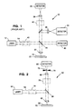
- Figure 1 is an illustration of the relevant portions of the above referenced device 10.
- Device 10 includes a laser 12 for generating a probe beam 14.
- a beam splitter 16 is used to redirect the beam down through a microscope objective lens 20 having a high numerical aperture.
- the lens 20 focuses the probe beam to a spot on the surface of the sample 18.
- the diameter of the spot is on the order of one micron.
- a stage 22 is provided to scan the sample with respect to the focused probe beam.
- a photodetector 26 is provided to measure the probe beam after it has reflected off the surface of the sample.
- a relay lens 28 is provided to expand and image the beam on the detector.
- Detector 26 includes an array of individual detector elements capable of measuring the areal intensity of various rays as a function of their position within the reflected probe beam. The position of the rays within the beam correspond to specific angles of incidence with respect to the surface of the sample.
- a processor (not shown) derives the thickness of the thin film layer based on the angular dependent intensity measurements.
- a second photodetector 34 is provided and arranged in a similar optical position as detector 26.
- a lens 36 is provided to image the beam on the detector 34.
- This second detector 34 is underfilled and configured to measure the full power of the reflected probe beam. The output from detector 34 is used to enhance the sensitivity of the evaluation.
- the light reaching either of the detectors 26 or 34 would be limited to that which has been reflected off the surface of the sample from within the focused spot.
- This light consists of portions of the probe beam that have been scattered or deflected out of the primary beam path. Such scattering effects can be produced by particulates in the air or on the lens. This effect can also be the result of imperfections in the lens or even in the beam itself.
- light energy can be measured by the detectors 26 and 34 from areas as far as 20 to 30 microns away from the edge of the focused spot. Since the device is intended to evaluate sample parameters only in the small one micron region, light reflected from areas outside the focused spot can improperly skew the measurement results.
- the subject invention is not limited to the apparatus described in the above cited application but might be used in any optical device where high resolution and high sensitivity are required.
- One example of another type of device where the subject invention could be utilized is described in U.S. Patent No. 5,042,951, issued August 27, 1991, assigned to the same assignee as the subject invention and incorporated herein by reference.
- the apparatus described in the latter application is an ellipsometric device which has a configuration similar in many respects to the device shown in Figure 1 herein.
- the principle difference is that the detector system is arranged to analyze the change in polarization state of various rays within the probe beam as a result of its reflection off the sample surface.
- the apparatus will be provided with a polarizing section 40 (shown in phantom line) and an analyzing section 42 (also shown in phantom line).
- the polarizing and analyzing sections can include polarizing elements which can be rotated about the propagation axis of the beam. By knowing the relative azimuthal positions of these rotatable elements in conjunction with the intensity measurement of detector 26, the change in polarization state of the beam can be determined. The latter analysis will also be adversely affected by detected light that has been reflected off the sample surface from areas outside of the focused probe beam spot.
- FIG. 1 illustrates one additional photodetector 46.
- Photodetector 46 is arranged to a measure a small portion of the probe beam that is transmitted through beam splitter 16. This portion of the light has not passed through lens 20 nor has it been reflected from the sample.
- the output of detector 46 is intended to monitor fluctuations in the output power of laser 12.
- the signal generated by detector 46 is used to normalize the output signals from detectors 26 and 34. In order to obtain an accurate normalization signal, it is necessary to insure that the portion of the probe beam striking detector 46 is the same as that which is passed through the aperture of the lens 18 to the sample. An approach for achieving that goal is also discussed below.
- an approach is provided to reduce the amount of detected light energy that has been reflected from a sample beyond the focused spot of the probe beam.
- the subject invention is implemented in an optical measurement apparatus which includes a laser for generating a probe beam.
- a high numerical aperture lens is provided for focusing the probe beam to a spot size of about one micron on the surface of the sample.
- a detector is provided for measuring some parameter of the reflected probe beam. As noted above, examples of this parameter could include the areal intensity of the beam, its full power or polarization state.
- a means for blocking light reflected from the surface of the sample beyond a predetermined distance from the center of the focused spot.
- This means includes a relay lens in front of the detector for imaging and magnifying the beam.
- a blocking member or spatial filter is also located in front of the detector and in the focal plane of the relay lens.
- the blocking member includes an aperture dimensioned to block the desired amount of stray or scattered light.
- the size of the area which is filtered is dependent on the magnification power of the relay lens and the size of the aperture.
- the lens power and aperture size should be selected to block substantially all of the light that has been reflected from the sample beyond the focused spot.
- a larger image area should be selected. Nonetheless, some spatial filtering is still desireable to avoid measurement errors.
- a detector is provided to monitor the power of the incident probe beam for normalizing the measurements made by the other detectors.
- an additional aperature should be provided in front of the incident power detector to insure that the power reaching the detector matches the power transmitted through the aperture of the microscope objective.
- Figure 1 is a schematic diagram of an optical measurement device of the prior art in which the subject invention can be implemented.
- Figure 2 is a schematic diagram of an optical measurement device in which the subject invention has been employed.
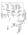
- Figure 3 is a schematic diagram of an optical measurement apparatus configured for measuring the thickness of thin films which includes the subject invention.
- Measurement apparatus 50 includes a laser 52 for generating a probe beam 54.
- a beam splitter 56 functions to redirect the beam towards the surface of the sample 58.
- Sample 58 rests on a movable stage 60.
- Probe beam 54 is focused on the surface of the sample through a high numerical aperture lens 62 to a spot size on the order of one micron in diameter.
- the stage 60 allows the probe beam to be scanned relative to the surface of the sample.
- Photodetector 66 is arranged to measure at least one parameter of the reflected probe beam.
- a relay lens 68 is provided to magnify and image the sample in the focal plane of the lens 68.
- the extent of the magnification of the image is given by the ratio of the focal length of lens 68 divided by the focal length of lens 62. In the preferred embodiment, this ratio is typically about 60 so that the image of the focused spot in this plane is about 60 microns in diameter.
- a blocking member 70 is located in the focal plane of the relay lens 68.
- Blocking member 70 includes an aperture 72 to define a spatial filter.
- the aperture 72 is dimensioned such that it will only transmit a portion of the relayed sample image.
- the amount of the image that is transmitted is defined by the size of the aperture divided by the magnification of the image. If it is desirable to substantially filter the image, an aperture of 400 microns could be used. This size aperture will reduce the filtered image field to about seven microns. In contrast, if the aperture were sized at 1500 microns, the image field would be about 24 microns in diameter.
- the use of the relay lens and blocking member substantially filter any spurious laser light that is scattered by either the optics of the system or the sample itself. This result is achieved because only light that is substantially spatially coherent will enter lens 68 and will be focused through the aperture 72. Any scattered light which is not traveling substantially parallel to the axis of the lens will strike portions of the blocking member and will not be transmitted through the aperture.
- photodetector 66 can be arranged to measure either the areal intensity or the full power of the beam.
- the photodetector 66 can also be used in an ellipsometer device.
- an ellipsometer will also include a polarizing section 76 (shown in phantom line) and an analyzing section 78 (also shown in phantom line).
- the polarizing and analyzing sections will include polarizing elements which can be rotated about the propagation axis of the beam. By knowing the relative azimuthal positions of these rotatable elements in conjunction with the intensity measurement of detector 66, the change in polarization state of the beam can be determined.
- the use of a spatial filter in an ellipsometer will improve accuracy by reducing the detection of spurious light scattered from the sample.
- Figure 3 is a schematic diagram illustrating the subject invention implemented in an apparatus 100 for measuring the thickness of thin films.
- This device is substantially similar to that described in U.S. Patent No. 4,999,014.
- this device includes some other modifications which have been developed since the filing of the latter patent application.
- the suggested source was a heliumneon gas laser.
- the laser source 102 is solid state diode laser which emits a linearly polarized beam 104.
- a Toshiba laser diode, TLD 9211 is used having a 3 milliwatt power output at 670nm.
- One advantage to using a diode laser is increased lifetime.
- Another significant advantage is that the coherence length is significantly shorter than a helium neon laser. Since the coherence length is shorter and therefore the divergence of the beam is greater, a much smaller percentage of the light reflected back towards the laser from the sample will enter the laser. Also, the reflected light will be less coherent when it enters the laser diode, thereby reducing optical feedback into the diode laser. Accordingly, it is unnecessary to use the more complicated filtering schemes described in the prior application and designed to prevent feedback that would cause instabilities in the laser.
- the remaining components in the apparatus are similar and include an imaging system, an angular sensitive photodetector, a full power detector, an incident power detector and an autofocus system.
- Probe beam 104 from the laser diode is turned with a 50/50 beam splitter 106.
- the beam 104 is then passed through a second 50/50 beam splitter 108 which is used to combine the beam with white light from source 110.
- the white light is used to image the sample using a vision system described in greater detail below.
- the probe beam 104 is then directed downwardly towards the sample by a 50/50 beam splitter 116 which also turns the white light down towards the sample. Upon return from the sample, part of the probe beam passes up through splitter 116 and will be measured by the detectors. Some of the white light from source 110 will be reflected back to the camera 196 of the vision system.
- the probe beam 104 is focused on the sample 118 to a spot size on the order of one micron through a high numerical aperture lens 120.
- Lens 120 is defined by a multielement microscope objective which has a focal length of 2.25 mm and includes an internal limiting aperture four millimeters in diameter.
- the lens has a high numerical aperture, preferably 0.95 NA, so the various rays in the focused beam will have a wide cone angle and a large spread of angles of incidence with respect to the sample surface.
- the accuracy of the evaluation of layer can be enhanced by maximizing the spread of angles of incidence that are available.
- Another advantage that is gained from overfilling lens 120 is that the light energy at the radially outer portion of the beam 104 is not used. Since the beam typically has a gaussian-like energy distribution, the energy in the radially outer portion thereof tends to fall off and be less uniform with respect to the rest of the beam.
- the fraction of the beam that passes through beam splitter 116 is monitored by detector 124.
- a blocking member 126 is placed in front of detector 124.
- the blocking member has an aperture 128 dimensioned to match the aperture in microscope objective 120. In this manner, the beam which passes through aperture 128 is the same portion of the beam which passes through the aperture of the lens 120 and back from the sample 118 to the other detectors.
- the sample 118 rests on a stage which provides X, Y, and rotational positional movement.
- the top stage 130 provides rotational movement as well as a vacuum chuck for holding down the sample.
- Stages 132 and 134 provide X and Y linear movement.
- a portion of the reflected probe beam 104 strikes 50/50 beam splitter 142 and is redirected to detector 140.
- detector 140 includes an array of individual elements capable of measuring the areal intensity of various rays as a function of their position within the reflected probe beam. The position of the rays within the beam correspond to specific angles of incidence with respect to the surface of the sample.
- a processor 144 derives the thickness of the thin film layer based on the angular dependent intensity measurements. As noted above, these measurements are normalized by the output of detector 124.
- the amount of light scattered from the sample surface which reaches the detector is reduced using a spatial filter arrangement.
- the spatial filter arrangement includes a relay lens 146 having a focal length of 140 mm.
- Relay lens 146 functions to magnify the image of the sample surface by a factor of about 60 in the image plane of the lens.
- a blocking member 148 is located in the image plane of lens 146 and includes an aperture 150 that is 1500 microns in diameter.
- Blocking member 148 can be defined by a metal plate having a thickness of two mils.
- This aperture will pass a 24 micron portion of the image of the sample and restrict any light scattered from areas on the sample outside of that range.
- This aperature size is preferable for detector 140 since interference effects created when the beam interacts with the thin film layer contain spatial information which must pass through this spatial filter aperature. The aperature is optimized to pass enough spatial information, but filter stray light from the sample.
- Photodetector 160 is provided for that purpose.
- the output of detector 160 is normalized by the processor 144 and used to enhance the accuracy of the evaluation.
- a portion of the reflected probe beam is directed towards detector 160 by 50/50 beam splitter 162.
- the beam is arranged to underfill detector 160.
- a spatial filter consisting of relay lens 164 and blocking member 166 located in the focal plane of the lens.
- lens 164 has a focal length of 140 mm and functions to magnify the image by a factor of about 60.
- Blocking member 166 includes an aperture 168 that is 400 microns in diameter and functions to reduce the image field down to about seven microns. In this manner, virtually no light which has been reflected from areas outside the focused spot will reach the detector. Accordingly, variations recorded by the detector, which can be as small as 1 in 10,000, can be attributed to the characteristics of the sample within the focused probe beam spot.
- an autofocus mechanism is used to maintain the spacing between the lens 120 and the sample 118 to be equal to the focal length of the lens. This distance can be maintained to less than one hundredth of a micron.
- the autofocus mechanism includes a servo motor 180 for varying the vertical position of the lens 120.
- the servo is driven by an analog detection loop which determines if the lens 120 is properly focusing the probe beam.
- a portion of the probe beam is transmitted by splitter 162 and is focused by a lens 182 through a chopper wheel 184 located in the focal plane of the lens.
- the light passing the chopper wheel 184 is imaged on a split-cell photodetector 186. If the lens 120 is out of focus, there will be a phase difference in the light striking the two sides of the split cell 186 which is detected by a phase detector 188.
- the phase difference is used as an input to an amplifier 190 which in turn drives the servo 180.
- This approach to autofocusing is known as the automated Foucault knife edge focus test.
- a vision system is provided to allow the operator to locate areas of interest on the sample.
- the vision system includes a white light source 110 which is directed to beam splitter 108 through a collimating lens 192.
- a mechanical shutter 194 for selectively blocking the light source is provided. In operation, shutter 194 is closed during measurement periods so that the white light will not reach any of the photodetectors. In this manner, the accuracy of the measurement can be enhanced by further reducing any spurious light.
- Some of the white light that has been directed down to the sample by splitter 116 will be reflected back along the same path passing through 50/50 splitters 108 and 106 to reach video camera 196.
- a lens 198 focuses the image provided to the camera.
- a variable laser wavelength cut-off filter 202 is provided to control the amount of probe beam light falling on the video camera.
- the device includes a laser for generating a probe beam which is tightly focused onto the surface of the sample.
- a detector is provided for monitoring a parameter of the reflected probe beam.
- a spatial filter is provided for reducing the amount of light energy reaching the detector that has been reflected from areas on the surface of the sample beyond the focused spot.
- the spatial filter includes a relay lens and a blocking member located in the focal plane of the relay lens.
- the blocking member includes an aperture dimensioned to block light reflected from the surface of the sample beyond a predetermined distance from the center of the focused spot. In this manner, greater sensitivity to sample characteristics within the highly focused spot is achieved.
Landscapes
- Physics & Mathematics (AREA)
- General Physics & Mathematics (AREA)
- Health & Medical Sciences (AREA)
- Life Sciences & Earth Sciences (AREA)
- Chemical & Material Sciences (AREA)
- Analytical Chemistry (AREA)
- Biochemistry (AREA)
- General Health & Medical Sciences (AREA)
- Immunology (AREA)
- Pathology (AREA)
- Length Measuring Devices By Optical Means (AREA)
- Testing Of Optical Devices Or Fibers (AREA)
Applications Claiming Priority (2)
| Application Number | Priority Date | Filing Date | Title |
|---|---|---|---|
| US670040 | 1991-03-15 | ||
| US07/670,040 US5159412A (en) | 1991-03-15 | 1991-03-15 | Optical measurement device with enhanced sensitivity |
Publications (2)
| Publication Number | Publication Date |
|---|---|
| EP0503874A2 true EP0503874A2 (de) | 1992-09-16 |
| EP0503874A3 EP0503874A3 (en) | 1993-07-07 |
Family
ID=24688730
Family Applications (1)
| Application Number | Title | Priority Date | Filing Date |
|---|---|---|---|
| EP19920301990 Withdrawn EP0503874A3 (en) | 1991-03-15 | 1992-03-09 | Optical measurement device with enhanced sensitivity |
Country Status (3)
| Country | Link |
|---|---|
| US (1) | US5159412A (de) |
| EP (1) | EP0503874A3 (de) |
| JP (1) | JPH05107035A (de) |
Cited By (11)
| Publication number | Priority date | Publication date | Assignee | Title |
|---|---|---|---|---|
| WO1998035328A3 (en) * | 1997-02-11 | 1998-12-23 | Scient Generics Ltd | Signalling system |
| WO1999002970A1 (en) * | 1997-07-11 | 1999-01-21 | Therma-Wave, Inc. | An apparatus for analyzing multi-layer thin film stacks on semiconductors |
| US5900939A (en) * | 1997-07-11 | 1999-05-04 | Therma-Wave, Inc. | Thin film optical measurement system and method with calibrating ellipsometer |
| EP1015869A4 (de) * | 1996-09-19 | 2000-07-05 | Molecular Dynamics Inc | Mikroabbildungssystem |
| WO2001020252A1 (en) | 1999-09-16 | 2001-03-22 | On-Line Technologies, Inc. | Method and apparatus for performing optical measurements of layers and surface properties |
| WO2001029836A1 (en) * | 1999-10-21 | 2001-04-26 | 3M Innovative Properties Company | Autofocus z stage |
| WO2001053806A1 (en) * | 2000-01-18 | 2001-07-26 | Radiometer Medical A/S | Apparatus, sample cuvette and method for optical measurements |
| US6278519B1 (en) | 1998-01-29 | 2001-08-21 | Therma-Wave, Inc. | Apparatus for analyzing multi-layer thin film stacks on semiconductors |
| WO2010124704A1 (en) * | 2009-04-30 | 2010-11-04 | Asml Netherlands B.V. | Metrology apparatus, lithography apparatus and method of measuring a property of a substrate |
| CN107765258A (zh) * | 2016-08-22 | 2018-03-06 | 原相科技股份有限公司 | 可用来判断参考物件或光源相对位置的光学侦测装置 |
| AT520307B1 (de) * | 2017-11-27 | 2019-03-15 | Riegl Laser Measurement Systems Gmbh | Optische Vorrichtung zum Detektieren eines an einem Fernziel reflektierten Lichtstrahls |
Families Citing this family (79)
| Publication number | Priority date | Publication date | Assignee | Title |
|---|---|---|---|---|
| US5270734A (en) * | 1991-08-23 | 1993-12-14 | Eastman Kodak Company | Auto-focus detector mask |
| US5528370A (en) * | 1993-06-09 | 1996-06-18 | The Perkin-Elmer Corporation | Apparatus and method for measuring variations in thickness of an optical interference element |
| US5412473A (en) * | 1993-07-16 | 1995-05-02 | Therma-Wave, Inc. | Multiple angle spectroscopic analyzer utilizing interferometric and ellipsometric devices |
| USRE38153E1 (en) * | 1993-11-09 | 2003-06-24 | Nova Measuring Instruments, Ltd. | Two-dimensional beam deflector |
| US5764365A (en) * | 1993-11-09 | 1998-06-09 | Nova Measuring Instruments, Ltd. | Two-dimensional beam deflector |
| IL107549A (en) | 1993-11-09 | 1996-01-31 | Nova Measuring Instr Ltd | Device for measuring the thickness of thin films |
| US6215587B1 (en) * | 1994-02-14 | 2001-04-10 | Robert R. Alfano | Microscope imaging inside highly scattering media |
| JP3404134B2 (ja) * | 1994-06-21 | 2003-05-06 | 株式会社ニュークリエイション | 検査装置 |
| WO1996012941A1 (en) * | 1994-10-21 | 1996-05-02 | Therma-Wave, Inc. | Spectroscopic ellipsometer |
| US5608526A (en) * | 1995-01-19 | 1997-03-04 | Tencor Instruments | Focused beam spectroscopic ellipsometry method and system |
| US6734967B1 (en) * | 1995-01-19 | 2004-05-11 | Kla-Tencor Technologies Corporation | Focused beam spectroscopic ellipsometry method and system |
| US6930813B1 (en) * | 2000-04-25 | 2005-08-16 | J.A. Woollam Co. Inc. | Spatial filter source beam conditioning in ellipsometer and the like systems |
| US5835228A (en) * | 1996-01-19 | 1998-11-10 | Dainippon Screen Mfg. Co., Ltd. | Image pickup apparatus, density measuring optical system and scanning optical microscope |
| DE19637131C2 (de) * | 1996-09-12 | 2001-02-01 | Autronic Melchers Gmbh | Einrichtung zum Beurteilen des Reflexionsverhaltens eines Objektes, insbesondere einer Flüssigkristallanzeige |
| US5859424A (en) * | 1997-04-08 | 1999-01-12 | Kla-Tencor Corporation | Apodizing filter system useful for reducing spot size in optical measurements and other applications |
| US5801817A (en) * | 1997-05-05 | 1998-09-01 | Umm Electronics Inc. | Method and apparatus for eliminating the effects of varying sample distance on optical measurements |
| US5991044A (en) * | 1997-06-04 | 1999-11-23 | Institute Of Microelectronics | Method and apparatus for determining characteristics of microstructures utilizing micro-modulation reflectance spectrometry |
| US5978074A (en) | 1997-07-03 | 1999-11-02 | Therma-Wave, Inc. | Apparatus for evaluating metalized layers on semiconductors |
| JP2002502980A (ja) * | 1998-02-10 | 2002-01-29 | イーワイ ラボラトリーズ インコーポレイテッド | 試料ホルダ起伏形状を補償し且つシステム・ノイズのロック除去を行う反射測定システム |
| IL123575A (en) * | 1998-03-05 | 2001-08-26 | Nova Measuring Instr Ltd | Method and apparatus for alignment of a wafer |
| US6885444B2 (en) | 1998-06-10 | 2005-04-26 | Boxer Cross Inc | Evaluating a multi-layered structure for voids |
| US6054868A (en) * | 1998-06-10 | 2000-04-25 | Boxer Cross Incorporated | Apparatus and method for measuring a property of a layer in a multilayered structure |
| US6049220A (en) | 1998-06-10 | 2000-04-11 | Boxer Cross Incorporated | Apparatus and method for evaluating a wafer of semiconductor material |
| US6320609B1 (en) * | 1998-07-10 | 2001-11-20 | Nanometrics Incorporated | System using a polar coordinate stage and continuous image rotation to compensate for stage rotation |
| US7295314B1 (en) | 1998-07-10 | 2007-11-13 | Nanometrics Incorporated | Metrology/inspection positioning system |
| JP4722244B2 (ja) | 1998-07-14 | 2011-07-13 | ノバ・メジャリング・インストルメンツ・リミテッド | 所定のフォトリソグラフィ工程に従って基板を加工する装置 |
| US6212961B1 (en) | 1999-02-11 | 2001-04-10 | Nova Measuring Instruments Ltd. | Buffer system for a wafer handling system |
| US6323951B1 (en) | 1999-03-22 | 2001-11-27 | Boxer Cross Incorporated | Apparatus and method for determining the active dopant profile in a semiconductor wafer |
| US6671051B1 (en) | 1999-09-15 | 2003-12-30 | Kla-Tencor | Apparatus and methods for detecting killer particles during chemical mechanical polishing |
| US6628397B1 (en) | 1999-09-15 | 2003-09-30 | Kla-Tencor | Apparatus and methods for performing self-clearing optical measurements |
| US6281027B1 (en) * | 1999-09-15 | 2001-08-28 | Therma-Wave Inc | Spatial averaging technique for ellipsometry and reflectometry |
| EP1251348A4 (de) * | 2000-01-28 | 2005-01-12 | Asahi Chemical Ind | Spektroskopischer analysator mit photothermischer wandlung |
| US6812047B1 (en) * | 2000-03-08 | 2004-11-02 | Boxer Cross, Inc. | Evaluating a geometric or material property of a multilayered structure |
| US6429943B1 (en) * | 2000-03-29 | 2002-08-06 | Therma-Wave, Inc. | Critical dimension analysis with simultaneous multiple angle of incidence measurements |
| US6532076B1 (en) * | 2000-04-04 | 2003-03-11 | Therma-Wave, Inc. | Method and apparatus for multidomain data analysis |
| US6693711B1 (en) | 2000-05-15 | 2004-02-17 | Regents Of The University Of Minnesota | Ellipsometer using radial symmetry |
| US6798511B1 (en) * | 2000-10-18 | 2004-09-28 | Regents Of The University Of Minnesota | Imaging ellipsometry |
| US6934024B2 (en) * | 2000-10-18 | 2005-08-23 | Regents Of The University Of Minnesota | Ellipsometry methods and apparatus using solid immersion tunneling |
| US6911349B2 (en) * | 2001-02-16 | 2005-06-28 | Boxer Cross Inc. | Evaluating sidewall coverage in a semiconductor wafer |
| US6812717B2 (en) * | 2001-03-05 | 2004-11-02 | Boxer Cross, Inc | Use of a coefficient of a power curve to evaluate a semiconductor wafer |
| US6514775B2 (en) | 2001-06-29 | 2003-02-04 | Kla-Tencor Technologies Corporation | In-situ end point detection for semiconductor wafer polishing |
| US6678046B2 (en) * | 2001-08-28 | 2004-01-13 | Therma-Wave, Inc. | Detector configurations for optical metrology |
| US6657714B2 (en) * | 2001-09-24 | 2003-12-02 | Applied Materials, Inc. | Defect detection with enhanced dynamic range |
| US6940592B2 (en) * | 2001-10-09 | 2005-09-06 | Applied Materials, Inc. | Calibration as well as measurement on the same workpiece during fabrication |
| US6813034B2 (en) * | 2002-02-05 | 2004-11-02 | Therma-Wave, Inc. | Analysis of isolated and aperiodic structures with simultaneous multiple angle of incidence measurements |
| US6958814B2 (en) * | 2002-03-01 | 2005-10-25 | Applied Materials, Inc. | Apparatus and method for measuring a property of a layer in a multilayered structure |
| US6971791B2 (en) * | 2002-03-01 | 2005-12-06 | Boxer Cross, Inc | Identifying defects in a conductive structure of a wafer, based on heat transfer therethrough |
| US7061627B2 (en) * | 2002-03-13 | 2006-06-13 | Therma-Wave, Inc. | Optical scatterometry of asymmetric lines and structures |
| US7671989B2 (en) * | 2002-06-24 | 2010-03-02 | J. A. Woollam Co., Inc. | Information maintenance during intensity attenuation in focused beams |
| US7046376B2 (en) * | 2002-07-05 | 2006-05-16 | Therma-Wave, Inc. | Overlay targets with isolated, critical-dimension features and apparatus to measure overlay |
| US6963393B2 (en) | 2002-09-23 | 2005-11-08 | Applied Materials, Inc. | Measurement of lateral diffusion of diffused layers |
| US6878559B2 (en) * | 2002-09-23 | 2005-04-12 | Applied Materials, Inc. | Measurement of lateral diffusion of diffused layers |
| KR100574963B1 (ko) * | 2003-12-29 | 2006-04-28 | 삼성전자주식회사 | 파장가변 레이저 장치를 구비한 광학적 임계치수 측정장치및 그 측정장치를 이용한 임계치수 측정방법 |
| US7026175B2 (en) * | 2004-03-29 | 2006-04-11 | Applied Materials, Inc. | High throughput measurement of via defects in interconnects |
| US7379185B2 (en) | 2004-11-01 | 2008-05-27 | Applied Materials, Inc. | Evaluation of openings in a dielectric layer |
| FR2880945B1 (fr) * | 2005-01-14 | 2007-04-06 | Essilor Int | Palpeur optique ainsi que dispositif et procede le mettant en oeuvre. |
| GB0706288D0 (en) * | 2007-03-30 | 2007-05-09 | Nightingale Eos Ltd | Method for measuring the thickness or curvature of thin films |
| US20100059657A1 (en) * | 2008-09-05 | 2010-03-11 | Nikon Corporation | System and Method Producing Data For Correcting Autofocus Error in An Imaging Optical System |
| WO2010037106A2 (en) | 2008-09-29 | 2010-04-01 | Kla-Tencor Corporation | Illumination subsystems of a metrology system, metrology systems, and methods for illuminating a specimen for metrology measurements |
| US9080991B2 (en) * | 2008-09-29 | 2015-07-14 | Kla-Tencor Corp. | Illuminating a specimen for metrology or inspection |
| US8441639B2 (en) * | 2009-09-03 | 2013-05-14 | Kla-Tencor Corp. | Metrology systems and methods |
| JP5696396B2 (ja) | 2010-08-16 | 2015-04-08 | ソニー株式会社 | 顕微鏡及びゴースト除去方法 |
| US9885656B2 (en) * | 2014-12-17 | 2018-02-06 | Kla-Tencor Corporation | Line scan knife edge height sensor for semiconductor inspection and metrology |
| CN106198568B (zh) * | 2015-05-24 | 2019-03-12 | 上海微电子装备(集团)股份有限公司 | 一种具有透明基底的薄膜的测量装置及测量方法 |
| US10088298B2 (en) | 2015-09-04 | 2018-10-02 | Kla-Tencor Corporation | Method of improving lateral resolution for height sensor using differential detection technology for semiconductor inspection and metrology |
| CN107192334A (zh) * | 2016-03-15 | 2017-09-22 | 信泰光学(深圳)有限公司 | 可调整光通量的测距装置 |
| US10066989B1 (en) | 2016-09-09 | 2018-09-04 | J.A. Woollam Co., Inc | Information maintenance, intensity attenuation, and angle/plane of incidence control in electromagentic beams |
| US10502830B2 (en) * | 2016-10-13 | 2019-12-10 | Waymo Llc | Limitation of noise on light detectors using an aperture |
| US10845470B2 (en) | 2016-11-16 | 2020-11-24 | Waymo Llc | Methods and systems for protecting a light detection and ranging (LIDAR) device |
| US10605984B2 (en) | 2016-12-01 | 2020-03-31 | Waymo Llc | Array of waveguide diffusers for light detection using an aperture |
| US10502618B2 (en) * | 2016-12-03 | 2019-12-10 | Waymo Llc | Waveguide diffuser for light detection using an aperture |
| US10422862B2 (en) | 2016-12-13 | 2019-09-24 | Sensl Technologies Ltd. | LiDAR apparatus |
| US20180164414A1 (en) * | 2016-12-13 | 2018-06-14 | Sensl Technologies Ltd. | LiDAR Apparatus |
| US20180164412A1 (en) * | 2016-12-13 | 2018-06-14 | Sensl Technologies Ltd. | LiDAR Apparatus |
| KR101898217B1 (ko) * | 2016-12-29 | 2018-09-12 | 엘지디스플레이 주식회사 | 검사장비 및 이를 이용한 검사방법 |
| US10698088B2 (en) * | 2017-08-01 | 2020-06-30 | Waymo Llc | LIDAR receiver using a waveguide and an aperture |
| US10890650B2 (en) * | 2017-09-05 | 2021-01-12 | Waymo Llc | LIDAR with co-aligned transmit and receive paths |
| US11561284B2 (en) | 2018-11-02 | 2023-01-24 | Waymo Llc | Parallax compensating spatial filters |
| CN115876795B (zh) * | 2021-09-30 | 2025-07-15 | 深圳中科飞测科技股份有限公司 | 检测方法和检测系统 |
Family Cites Families (4)
| Publication number | Priority date | Publication date | Assignee | Title |
|---|---|---|---|---|
| JPH0627706B2 (ja) * | 1985-04-25 | 1994-04-13 | オリンパス光学工業株式会社 | 反射率測定装置 |
| JPH0252205A (ja) * | 1988-08-17 | 1990-02-21 | Dainippon Screen Mfg Co Ltd | 膜厚測定方法 |
| US5042951A (en) * | 1989-09-19 | 1991-08-27 | Therma-Wave, Inc. | High resolution ellipsometric apparatus |
| US4999014A (en) * | 1989-05-04 | 1991-03-12 | Therma-Wave, Inc. | Method and apparatus for measuring thickness of thin films |
-
1991
- 1991-03-15 US US07/670,040 patent/US5159412A/en not_active Expired - Lifetime
-
1992
- 1992-03-09 EP EP19920301990 patent/EP0503874A3/en not_active Withdrawn
- 1992-03-16 JP JP4090233A patent/JPH05107035A/ja active Pending
Cited By (29)
| Publication number | Priority date | Publication date | Assignee | Title |
|---|---|---|---|---|
| EP1015869A4 (de) * | 1996-09-19 | 2000-07-05 | Molecular Dynamics Inc | Mikroabbildungssystem |
| US6624916B1 (en) | 1997-02-11 | 2003-09-23 | Quantumbeam Limited | Signalling system |
| WO1998035328A3 (en) * | 1997-02-11 | 1998-12-23 | Scient Generics Ltd | Signalling system |
| US6411385B2 (en) | 1997-07-11 | 2002-06-25 | Therma-Wave, Inc. | Thin film optical measurement system and method with calibrating ellipsometer |
| WO1999002970A1 (en) * | 1997-07-11 | 1999-01-21 | Therma-Wave, Inc. | An apparatus for analyzing multi-layer thin film stacks on semiconductors |
| US5900939A (en) * | 1997-07-11 | 1999-05-04 | Therma-Wave, Inc. | Thin film optical measurement system and method with calibrating ellipsometer |
| US6934025B2 (en) | 1997-07-11 | 2005-08-23 | Therma-Wave, Inc. | Thin film optical measurement system and method with calibrating ellipsometer |
| US6753962B2 (en) | 1997-07-11 | 2004-06-22 | Therma-Wave, Inc. | Thin film optical measurement system and method with calibrating ellipsometer |
| US6515746B2 (en) | 1997-07-11 | 2003-02-04 | Therma-Wave, Inc. | Thin film optical measurement system and method with calibrating ellipsometer |
| US6304326B1 (en) | 1997-07-11 | 2001-10-16 | Therma-Wave, Inc. | Thin film optical measurement system and method with calibrating ellipsometer |
| US6278519B1 (en) | 1998-01-29 | 2001-08-21 | Therma-Wave, Inc. | Apparatus for analyzing multi-layer thin film stacks on semiconductors |
| US6774997B2 (en) | 1998-01-29 | 2004-08-10 | Therma-Wave, Inc. | Apparatus for analyzing multi-layer thin film stacks on semiconductors |
| US6297880B1 (en) | 1998-01-29 | 2001-10-02 | Therma-Wave, Inc. | Apparatus for analyzing multi-layer thin film stacks on semiconductors |
| US6922244B2 (en) | 1998-01-29 | 2005-07-26 | Therma-Wave, Inc. | Thin film optical measurement system and method with calibrating ellipsometer |
| US6417921B2 (en) | 1998-01-29 | 2002-07-09 | Therma-Wave, Inc. | Apparatus for analyzing multi-layer thin film stacks on semiconductors |
| US6567213B2 (en) | 1998-01-29 | 2003-05-20 | Therma-Wave, Inc. | Apparatus for analyzing multi-layer thin film stacks on semiconductors |
| WO2001020252A1 (en) | 1999-09-16 | 2001-03-22 | On-Line Technologies, Inc. | Method and apparatus for performing optical measurements of layers and surface properties |
| EP1212580A4 (de) * | 1999-09-16 | 2003-04-02 | Mks Instr Inc | Methode und apparat fur optischen messungen von schichten und oberflacheneigenschaften |
| US6717124B2 (en) | 1999-10-21 | 2004-04-06 | 3M Innovative Properties Company | Autofocus z stage |
| WO2001029836A1 (en) * | 1999-10-21 | 2001-04-26 | 3M Innovative Properties Company | Autofocus z stage |
| US6548795B1 (en) | 1999-10-21 | 2003-04-15 | 3M Innovative Properties Company | Autofocus Z stage |
| US6943883B2 (en) | 2000-01-18 | 2005-09-13 | Radiometer Medical A/S | Apparatus, sample cuvette and method for optical measurements |
| WO2001053806A1 (en) * | 2000-01-18 | 2001-07-26 | Radiometer Medical A/S | Apparatus, sample cuvette and method for optical measurements |
| WO2010124704A1 (en) * | 2009-04-30 | 2010-11-04 | Asml Netherlands B.V. | Metrology apparatus, lithography apparatus and method of measuring a property of a substrate |
| CN107765258A (zh) * | 2016-08-22 | 2018-03-06 | 原相科技股份有限公司 | 可用来判断参考物件或光源相对位置的光学侦测装置 |
| CN107765258B (zh) * | 2016-08-22 | 2021-02-05 | 原相科技股份有限公司 | 可用来判断参考物件或光源相对位置的光学侦测装置 |
| AT520307B1 (de) * | 2017-11-27 | 2019-03-15 | Riegl Laser Measurement Systems Gmbh | Optische Vorrichtung zum Detektieren eines an einem Fernziel reflektierten Lichtstrahls |
| AT520307A4 (de) * | 2017-11-27 | 2019-03-15 | Riegl Laser Measurement Systems Gmbh | Optische Vorrichtung zum Detektieren eines an einem Fernziel reflektierten Lichtstrahls |
| US11360194B2 (en) | 2017-11-27 | 2022-06-14 | Riegl Laser Measurement Systems Gmbh | Optical device for detecting a reflected light beam |
Also Published As
| Publication number | Publication date |
|---|---|
| US5159412A (en) | 1992-10-27 |
| JPH05107035A (ja) | 1993-04-27 |
| EP0503874A3 (en) | 1993-07-07 |
Similar Documents
| Publication | Publication Date | Title |
|---|---|---|
| US5159412A (en) | Optical measurement device with enhanced sensitivity | |
| US5576831A (en) | Wafer alignment sensor | |
| EP1131623B1 (de) | Nachweissystem für nanometer genaue topographische messung reflektiver oberflächen | |
| US5929983A (en) | Optical apparatus for determining the height and tilt of a sample surface | |
| US5610719A (en) | Displacement detection system | |
| US11255796B2 (en) | Region prober optical inspector | |
| US7205518B2 (en) | Method and arrangement for focusing in an optical measurement | |
| US11852592B2 (en) | Time domain multiplexed defect scanner | |
| US12146732B2 (en) | Surface contour measurement | |
| US12146830B2 (en) | Slope, p-component and s-component measurement | |
| US12147033B2 (en) | Scanning micro profiler | |
| EP0396409B1 (de) | Ellipsometrische Vorrichtung mit hohem Auflösungsvermögen | |
| US11988615B2 (en) | Region prober optical inspector | |
| JPH0330085B2 (de) | ||
| US10767977B1 (en) | Scattered radiation defect depth detection | |
| US4976543A (en) | Method and apparatus for optical distance measurement | |
| JP3934051B2 (ja) | 表面欠陥の測定 | |
| WO2003060589A1 (en) | Auto focussing device and method | |
| US12130243B2 (en) | Angle independent optical surface inspector | |
| US10648928B1 (en) | Scattered radiation optical scanner | |
| JPH05312538A (ja) | 3次元形状測定装置 | |
| US20250093274A1 (en) | Dual scan beam separation with independent angle of incidence defect scanner and optical inspector | |
| WO2025117560A1 (en) | Dual scan beam separation with independent angle of incidence defect scanner and optical inspector | |
| US10641713B1 (en) | Phase retardance optical scanner | |
| JPH0471453B2 (de) |
Legal Events
| Date | Code | Title | Description |
|---|---|---|---|
| PUAI | Public reference made under article 153(3) epc to a published international application that has entered the european phase |
Free format text: ORIGINAL CODE: 0009012 |
|
| AK | Designated contracting states |
Kind code of ref document: A2 Designated state(s): DE FR GB NL |
|
| PUAL | Search report despatched |
Free format text: ORIGINAL CODE: 0009013 |
|
| AK | Designated contracting states |
Kind code of ref document: A3 Designated state(s): DE FR GB NL |
|
| 17P | Request for examination filed |
Effective date: 19931217 |
|
| 17Q | First examination report despatched |
Effective date: 19941206 |
|
| RAP1 | Party data changed (applicant data changed or rights of an application transferred) |
Owner name: THERMA-WAVE, INC. (A DELAWARE CORPORATION) |
|
| GRAG | Despatch of communication of intention to grant |
Free format text: ORIGINAL CODE: EPIDOS AGRA |
|
| GRAG | Despatch of communication of intention to grant |
Free format text: ORIGINAL CODE: EPIDOS AGRA |
|
| GRAG | Despatch of communication of intention to grant |
Free format text: ORIGINAL CODE: EPIDOS AGRA |
|
| GRAH | Despatch of communication of intention to grant a patent |
Free format text: ORIGINAL CODE: EPIDOS IGRA |
|
| 18D | Application deemed to be withdrawn |
Effective date: 19980514 |
|
| P01 | Opt-out of the competence of the unified patent court (upc) registered |
Effective date: 20230525 |