EP0503117A1 - Processor circuit - Google Patents
Processor circuit Download PDFInfo
- Publication number
- EP0503117A1 EP0503117A1 EP91103867A EP91103867A EP0503117A1 EP 0503117 A1 EP0503117 A1 EP 0503117A1 EP 91103867 A EP91103867 A EP 91103867A EP 91103867 A EP91103867 A EP 91103867A EP 0503117 A1 EP0503117 A1 EP 0503117A1
- Authority
- EP
- European Patent Office
- Prior art keywords
- input
- output
- register
- test
- multiplexer
- Prior art date
- Legal status (The legal status is an assumption and is not a legal conclusion. Google has not performed a legal analysis and makes no representation as to the accuracy of the status listed.)
- Granted
Links
Images

Classifications
-
- G—PHYSICS
- G06—COMPUTING; CALCULATING OR COUNTING
- G06F—ELECTRIC DIGITAL DATA PROCESSING
- G06F11/00—Error detection; Error correction; Monitoring
- G06F11/22—Detection or location of defective computer hardware by testing during standby operation or during idle time, e.g. start-up testing
- G06F11/2205—Detection or location of defective computer hardware by testing during standby operation or during idle time, e.g. start-up testing using arrangements specific to the hardware being tested
- G06F11/2236—Detection or location of defective computer hardware by testing during standby operation or during idle time, e.g. start-up testing using arrangements specific to the hardware being tested to test CPU or processors
Landscapes
- Engineering & Computer Science (AREA)
- General Engineering & Computer Science (AREA)
- Theoretical Computer Science (AREA)
- Computer Hardware Design (AREA)
- Quality & Reliability (AREA)
- Physics & Mathematics (AREA)
- General Physics & Mathematics (AREA)
- Test And Diagnosis Of Digital Computers (AREA)
- Tests Of Electronic Circuits (AREA)
Abstract
Description
Die Erfindung betrifft eine zum Baugruppenselbsttest geeignete Prozessorschaltung.The invention relates to a processor circuit suitable for module self-testing.
Die zunehmend dichtere Plazierung der Bauteile auf den Montageträgern bei den Baugruppen läßt eine Kontaktierung durch Klammern oder Prüfspitzen für den Baugruppentest in Zukunft nicht länger zu. Somit sinken die Möglichkeiten einer Qualitätskontrolle und einer schnellen Fehlerdiagnose vorort. Aus diesem Grunde wurde von der Joint Test Action Group (JTAG) ein Standard Test Access Port und eine Boundary-Scan Architektur definiert (vgl. IEEE Standard 1149.1/D6, Standard Test Access Port and Boundary-Scan Architecture, Draft, November 22, 1989).The increasingly denser placement of the components on the mounting brackets for the assemblies will no longer allow contacting them with clamps or test probes for the assembly test in the future. This reduces the possibilities for quality control and quick fault diagnosis on site. For this reason, the Joint Test Action Group (JTAG) defined a standard test access port and a boundary-scan architecture (see IEEE Standard 1149.1 / D6, Standard Test Access Port and Boundary-Scan Architecture, Draft, November 22, 1989 ).
Bei einer diesem Standard entsprechenden Schaltung werden zum Testen Befehle und zugehörige Daten in eine Schaltungskomponente seriell eingelesen und nach Ausführung des Befehls das Ergebnis seriell ausgelesen. Die Abfolge der einzelnen Operationen wird durch einen Busmaster überwacht und gesteuert. Als Busmaster fungiert entweder eine automatische Testeinrichtung oder eine Schaltungskomponente, die mit einem, zu einer umfassenden Wartungseinrichtung gehörenden Testbus gekoppelt ist. Zur Überwachung und Steuerung werden Testmodusauswahleingänge und Testtakteingänge der einzelnen Schaltungskomponenten mit dem Busmaster verbunden. Ausgehend von einem Initialisierungszustand, in dem die standardgemäße Schaltung inaktiv ist, wird anschließend eine festgelegte Abfolge von Operationen abgearbeitet.In a circuit conforming to this standard, commands and associated data are read in serially into a circuit component for testing and the result is read out serially after the command has been executed. The sequence of the individual operations is monitored and controlled by a bus master. Either an automatic test device or a circuit component, which is coupled to a test bus belonging to a comprehensive maintenance device, functions as the bus master. Test mode selection inputs and test clock inputs of the individual circuit components are connected to the bus master for monitoring and control. Starting from an initialization state in which the standard circuit is inactive, a defined sequence of operations is then processed.
Zunächst wird im allgemeinen der Befehlscode der einzelnen durchzuführenden Operationen in die jeweiligen Schaltungskomponenten geladen. Eine dem genannten Standard entsprechende Testlogik ist dabei derart ausgelegt, daß das Schieben der Befehlsworte auf Schaltungsblöcke, die durch diesen Befehl gesteuert werden, keinen Einfluß hat. Die an diese Schaltungsblöcke übertragenen Befehle werden nur dann geändert, wenn der Schiebevorgang beendet ist.First, the command code of the individual operations to be performed is generally loaded into the respective circuit components. A test logic corresponding to the standard mentioned is designed such that the pushing of the Command words have no effect on circuit blocks controlled by this command. The commands transmitted to these circuit blocks are changed only when the shift is finished.
Nachdem das Befehlswort geladen worden ist, wird die ausgewählte Testschaltung aktiviert. In einigen Fällen sind jedoch, bevor ein Abarbeiten erfolgen kann, Datenworte in die Testschaltung einzugeben. Das Laden der Datenworte erfolgt dabei prinzipiell in gleicher Weise wie zuvor das Laden der Befehlsworte, wobei die Datenworte keinen Einfluß auf die Befehlsworte haben.After the command word has been loaded, the selected test circuit is activated. In some cases, however, before processing can take place, data words have to be entered into the test circuit. In principle, the data words are loaded in the same way as the command words were previously loaded, the data words having no influence on the command words.
Anschließend wird der geladene Befehl gegebenenfalls unter Berücksichtigung der eingegebenen Daten abgearbeitet und das Ergebnis durch Schieben aus der jeweiligen Schaltungskomponente an den Busmaster oder mittels des Busmasters seriell ausgelesen. In Fällen in denen der Befehl gleichbleibt und sich nur die Daten ändern, werden lediglich die neuen Daten in die jeweilige Schaltungskomponente geladen während gleichzeitig das aus den vorherigen Daten ermittelte Ergebnis ausgelesen wird. Ein erneutes Laden des Befehls ist dabei nicht notwendig.The loaded command is then processed, taking into account the data entered, if necessary, and the result is read out serially by pushing from the respective circuit component to the bus master or by means of the bus master. In cases where the command remains the same and only the data changes, only the new data is loaded into the respective circuit component, while the result determined from the previous data is read out at the same time. It is not necessary to reload the command.
Damit wird nun die Beobachbarkeit und die Stimmulierbarkeit aller erfaßten Leitungen und Schaltungsblöcke erzielt sowie eine einfache, kostengünstige Schnittstelle, beispielsweise zu automatischen Testeinrichtungen, mit der Möglichkeit einer Ferndiagnose geschaffen.The observability and tunability of all detected lines and circuit blocks is now achieved, and a simple, inexpensive interface, for example to automatic test devices, with the possibility of remote diagnosis is created.
In Regel 3.1.1 des obengenannten Standards ist jedoch ausdrücklich gefordert, daß die Anschlüsse des definierten Test Access Ports nicht für andere Zwecke benutzt werden dürfen. Damit ist es zum Beispiel nicht möglich, bei einer Baugruppe mit Prozessor zum einen diesen die Testleitungen für einen Baugruppenselbsttest stimmulieren zu lassen und zum anderen trotzdem einen Fertigungstest durch eine externe Testlogik über denselben Testbus durchzuführen. Durch die Stimmulierung im Fall eines Selbsttests würden die an der Baugruppe vorzusehenden Eingangsanschlüsse zu Ausgangssanschlüssen und umgekehrt.However, rule 3.1.1 of the above-mentioned standard expressly requires that the connections of the defined test access port must not be used for other purposes. It is therefore not possible, for example, for a module with a processor to have the test lines stimulated for a module self-test on the one hand, and nevertheless to carry out a production test by means of an external test logic via the same test bus. By the stimulation in the case of a Self-tests would convert the input connections to be provided on the module to output connections and vice versa.
Aufgabe der Erfindung ist es daher, eine Prozessorschaltung anzugeben, die unter Einhaltung der in obengenanntem Standard aufgeführten Bedingungen neben dem Test der Prozessorschaltung selbst auch einen Baugruppenselbsttest und einen Baugruppenfertigungstest ermöglicht.The object of the invention is therefore to provide a processor circuit which, in compliance with the conditions listed in the above-mentioned standard, also enables a module self-test and a module production test in addition to the test of the processor circuit itself.
Die Aufgabe wird durch eine Prozessorschaltung gemäß Patentanspruch 1 gelöst. Ausgestaltungen und Weiterbildungen des Erfindungsgedankens sind Gegenstand von Unteransprüchen.The object is achieved by a processor circuit according to
Die Erfindung wird nachfolgend anhand des in der einzigen Figur der Zeichnung dargestellten Ausführungsbeispiels näher erläutert.The invention is explained in more detail below with reference to the embodiment shown in the single figure of the drawing.
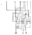
Zur Einhaltung von Formerfordernissen ist die einzige Figur entlang gekennzeichneter Schnittpunkte a bis i in zwei Teilfiguren aufgespalten.To comply with formal requirements, the single figure is split into two sub-figures along marked intersection points a to i.
Eine erfindungsgemäße Prozessorschaltung weist beispielsweise einen Demultiplexer D6 auf, dessen Eingang mit einem externen Testdateneingang TDI verbunden ist. An jeweils einem Ausgang des Demultiplexers D6 sind die Eingänge eines Befehlsregisters INSTR2, eines Bypassregisters BYPR2, eines Teststatusregisters TSR und eines Testinforegisters TIR angeschlossen, wobei das Teststatusregister TSR und das Testinforegister TIR zusätzlich mit einem internen bidirektionalen Bus IBUS gekoppelt sind. Die Ausgänge des Befehlsregisters INSTR2, des Bypassregisters BYPR2, des Teststatusregisters TSR und des Testinforegisters TIR sind auf jeweils einen Eingang eines Multiplexers M13 geführt. Ein weiter Eingang des Multiplexers M13 ist zudem mit einem Ausgang des Demultiplexers D6 verbunden. Ein Multiplexer M14 ist eingangsseitig zum einen mit dem Ausgang des Multiplexers M13 und zum anderen mit einer internen Testdatenausgangsleitung TDOI gekoppelt. Der Ausgang des Multiplexers M14 ist mit einem externen Testdatenausgang TDO verbunden.A processor circuit according to the invention has, for example, a demultiplexer D6, the input of which is connected to an external test data input TDI. The inputs of a command register INSTR2, a bypass register BYPR2, a test status register TSR and a test information register TIR are connected to each output of the demultiplexer D6, the test status register TSR and the test information register TIR additionally being coupled to an internal bidirectional bus IBUS. The outputs of the command register INSTR2, the bypass register BYPR2, the test status register TSR and the test information register TIR are each fed to an input of a multiplexer M13. Another input of the multiplexer M13 is also connected to an output of the demultiplexer D6. On the input side, a multiplexer M14 is coupled on the one hand to the output of the multiplexer M13 and on the other hand to an internal test data output line TDOI. The output of the multiplexer M14 is connected to an external test data output TDO.
Weiterhin ist ein Testcontroller TAPC2 vorgesehen, dessen einer Eingang an einen externen Testmodusauswahleingang TMS und dessen anderer Eingang an einen externen Testtakteingang TCK angeschlossen ist, und ein Testcontrollregister TCR, das an den internen bidirektionalen Bus IBUS angeschlossen ist, vorgesehen. Mit dem Ausgang des Testcontrollregisters TCR ist ebenso wie mit den Ausgängen des Testcontrollers TAPC2 und des Befehlsregisters INSTR2 ein Decoder DEC2 über interne unidirektionale Busleitungen verschaltet. Die Ausgänge des Decoders DEC2 sind an eine interne Prozessorresetleitung PRI, eine interne Prozessorinterruptleitung PII und eine Testlogikresetleitung TLR angeschlossen.Furthermore, a test controller TAPC2 is provided, one input of which is connected to an external test mode selection input TMS and the other input of which is connected to an external test clock input TCK, and a test control register TCR which is connected to the internal bidirectional bus IBUS. A decoder DEC2 is connected to the output of the test control register TCR as well as to the outputs of the test controller TAPC2 and the command register INSTR2 via internal unidirectional bus lines. The outputs of the decoder DEC2 are connected to an internal processor reset line PRI, an internal processor interrupt line PII and a test logic reset line TLR.
Neben dem Teststatusregister TSR, dem Testinforegister TIR und dem Testcontrollregister TCR sind zudem ein interner Speicher IMEM, ein mehrere Ein- und Ausgabeleitungen aufweisender Port PORT und ein Prozessorkern PC, der zusätzlich an die interne Prozessorresetleitung PRI, die interne Prozessorinterruptleitung PII, die Testlogikresetleitung TLR und eine Zellenleseleitung CER angeschlossen ist, mit dem internen bidirektionalen Bus IBUS gekoppelt. Der interne Speicher IMEM ist zur Aufnahme des Prozessorprogramms und zur Aufnahme von Daten vorgesehen und kann sowohl als flüchtiger als auch als nichtflüchtiger Speicher ausgelegt sein.In addition to the test status register TSR, the test information register TIR and the test control register TCR, there is also an internal memory IMEM, a port PORT with multiple input and output lines and a processor core PC that also connects to the internal processor reset line PRI, the internal processor interrupt line PII, the test logic reset line TLR and a cell reading line CER is connected, coupled to the internal bidirectional bus IBUS. The internal memory IMEM is provided for receiving the processor program and for receiving data and can be designed both as volatile and as non-volatile memory.
Weiterhin ist ein Multiplexer M1 vorgesehen, dessen einer Eingang an den Ausgang des Multiplexers M13 und dessen anderer Eingang an einer ersten Eingabeleitung des Ports PORT angeschlossen ist. Der Ausgang des Multiplexers M1 über eine interne Testdateneingangsleitung TDII ist auf den Eingang eines Demultiplexers D1 geführt. An Ausgängen des Demultiplexers D1 sind der serielle Eingang eines Boundary-Scan-Registers BSR1, ein Befehlsregister INSTR1, ein Bypassregister BYPR1, ein Herstellerregister MAR und ein Multiplexer M2 angeschlossen. Dem Boundary-Scan-Register BSR1 ist ein Demultiplexer D2 nachgeschaltet. Ein Ausgang des Demultiplexers D2 ist mit einem Serielleingang einer Registerzelle T1 verbunden, während ein Paralleleingang mit einem externen Takteingang CLK verschaltet ist. Der andere Ausgang des Demultiplexers D2 ist auf einen Eingang eines Multiplexers M3 geführt, dessen anderer Eingang an einen Seriellausgang der Speicherzelle T1 angeschlossen ist. Dem Multiplexer M3 ist ein Boundary-Scan-Register BSR2 nachgeschaltet, dem wiederum ein Demultiplexer D3 folgt. An einem Ausgang des Demultiplexers D3 ist dabei ein Boundary-Scan-Register BSR3 angeschlossen, dessen serieller Ausgang wiederum auf einen Multiplexer M4 geführt ist. Der andere Eingang des Multiplexers M4 ist mit einem anderen Eingang des Demultiplexers D3 verbunden. Neben der seriellen Ein- und Ausgabe ist beim Boundary-Scan-Register BSR3 beim Ausführungsbeispiel auch ein paralleler Zugriff möglich. Dazu ist das Boundary-Scan-Register BSR3 zum einen an den internen bidirektionalen Bus IBUS und zum anderen an einen externen bidirektionalen Bus EBUS angeschlossen. Beide Busse sind hier dabei zur Übertragung von Daten, Adressen und Steuersignalen in beiden Richtungen vorgesehen. Dem Multiplexer M4 schließt sich ein Boundary-Sscan-Register BSR4 an. Dem Boundary-Scan-Register BSR4 ist ein Demultiplexer D4 nachgeschaltet. Ein Ausgang des Demultiplexers D4 ist auf einen Serielleingang einer Registerzelle T2 geführt, deren Paralleleingang mit einem zusätzlichen externen Testmodusauswahleingang TMSH verbunden ist. Einem Seriellausgang der Registerzelle T2 ist ein Demultiplexer D5 nachgeschaltet, dessen einer Ausgang mit einem Ausgang eines Multiplexers M5 verschaltet ist. Ein anderer Eingang des Multiplexers M5 ist an die interne Testdatenausgangsleitung TDOI angeschlossen.Furthermore, a multiplexer M1 is provided, one input of which is connected to the output of the multiplexer M13 and the other input of which is connected to a first input line of the port PORT. The output of the multiplexer M1 via an internal test data input line TDII is led to the input of a demultiplexer D1. The outputs of the demultiplexer D1 are connected to the serial input of a boundary scan register BSR1, an instruction register INSTR1, a bypass register BYPR1, a manufacturer register MAR and a multiplexer M2. A demultiplexer D2 is connected downstream of the boundary scan register BSR1. An output of the demultiplexer D2 is connected to a serial input of a register cell T1 while an Parallel input is connected to an external clock input CLK. The other output of the demultiplexer D2 is connected to an input of a multiplexer M3, the other input of which is connected to a serial output of the memory cell T1. The multiplexer M3 is followed by a boundary scan register BSR2, which in turn is followed by a demultiplexer D3. A boundary scan register BSR3 is connected to an output of the demultiplexer D3, the serial output of which in turn is routed to a multiplexer M4. The other input of the multiplexer M4 is connected to another input of the demultiplexer D3. In addition to the serial input and output in the boundary scan register BSR3, parallel access is also possible in the exemplary embodiment. For this purpose, the boundary scan register BSR3 is connected on the one hand to the internal bidirectional bus IBUS and on the other hand to an external bidirectional bus EBUS. Both buses are intended to transmit data, addresses and control signals in both directions. The multiplexer M4 is followed by a boundary scan register BSR4. The boundary scan register BSR4 is followed by a demultiplexer D4. An output of the demultiplexer D4 is led to a serial input of a register cell T2, the parallel input of which is connected to an additional external test mode selection input TMSH. A serial output of the register cell T2 is followed by a demultiplexer D5, the output of which is connected to an output of a multiplexer M5. Another input of the multiplexer M5 is connected to the internal test data output line TDOI.
Ein Parallelausgang einer Registerzelle T3, deren Serielleingang mit dem Ausgang des Multiplexers M5 verbunden ist, sind an einen externen Testausgang TO bzw. an eine zweite Eingabeleitung des Ports PORT angeschlossen. Es folgen eine Registerzelle T4, deren Serielleingang mit einem Seriellausgang der Registerzelle T3 und deren Parallelausgang mit einem externen Testmodusauswahlausgang TMSO verbunden ist, und eine Registerzelle T5, deren Serielleingang mit einem Seriellausgang der Registerzelle T4 verbunden ist und deren Parallelausgang an einen externen Testtaktausgang TCKO angeschlossen ist. Der Parallelausgang der dritten Registerzelle T3 ist zudem mit einem Eingang eines Multiplexers M6 verschaltet, dessen anderer Eingang mit einem externen Testeingang TI verbunden ist. Eine Registerzelle T6 ist über einen Serielleingang mit einem Seriellausgang der Registerzelle T5 und über einen Paralleleingang mit dem Ausgang des Multiplexers M6 gekoppelt. Ihr Parallelausgang ist an die erste Eingabeleitung des Ports PORT angeschlossen. Es folgt ein Multiplexer M2, dessen einer Eingang an die erste Ausgabeleitung des Ports PORT und dessen anderer Eingang an einem weiteren Ausgang des Demultiplexers D1 angeschlossen ist. Sein Ausgang ist mit einem Paralleleingang der Registerzelle T3 verbunden. Außerdem ist ein Multiplexer M7, dessen einer Eingang an die zweite Ausgabeleitung des Ports PORT und dessen anderer Eingang mit einem Parallelausgang der Registerzelle T2 verbunden ist sowie dessen Ausgang mit einem Paralleleingang der Registerzelle T4 gekoppelt ist, und ein Multiplexer M8, dessen einer Eingang an die dritte Ausgabeleitung des Ports PORT und dessen anderer Eingang an den externen Testtakteingang TCK angeschlossen ist und dessen Ausgang mit einem Paralleleingang der fünften Registerzelle T5 verbunden ist, vorgesehen. Ein Seriellausgang der Registerzelle T6 ist auf einen Eingang eines Multiplexers M9 geführt, bei dem jeweils ein weiterer Eingang an jeweils einen anderen Ausgang der Demultiplexer D5 und D6 angeschlossen ist. Dem Multiplexer M9 ist ein Boundary-Scan-Register BSR5 nachgeschaltet. Der Ausgang des Boundary-Scan-Registers BSR5 ist auf einen Multiplexer M10 geführt, bei weitere Eingänge jeweils mit Ausgängen des Befehlsregisters INSTR1, des Bypassregister BYPR1 und dem Herstellerregister MAR sowie mit der ersten Eingabeleitung des Ports PORT verbunden sind und dessen Ausgang an die interne Testdatenausgangsleitung TDOI angeschlossen ist.A parallel output of a register cell T3, the serial input of which is connected to the output of the multiplexer M5, is connected to an external test output TO or to a second input line of the port PORT. This is followed by a register cell T4, whose serial input is connected to a serial output of the register cell T3 and whose parallel output is connected to an external test mode selection output TMSO, and a register cell T5, whose serial input is connected to a serial output Register cell T4 is connected and its parallel output is connected to an external test clock output TCKO. The parallel output of the third register cell T3 is also connected to an input of a multiplexer M6, the other input of which is connected to an external test input TI. A register cell T6 is coupled via a serial input to a serial output of the register cell T5 and via a parallel input to the output of the multiplexer M6. Its parallel output is connected to the first input line of the PORT port. A multiplexer M2 follows, one input of which is connected to the first output line of the port PORT and the other input of which is connected to a further output of the demultiplexer D1. Its output is connected to a parallel input of the register cell T3. In addition, there is a multiplexer M7, one input of which is connected to the second output line of the port PORT and the other of which is connected to a parallel output of the register cell T2, and the output of which is coupled to a parallel input of the register cell T4, and a multiplexer M8, one input of which is connected to the third output line of the port PORT and its other input is connected to the external test clock input TCK and its output is connected to a parallel input of the fifth register cell T5. A serial output of the register cell T6 is connected to an input of a multiplexer M9, in which a further input is connected to a different output of the demultiplexers D5 and D6. The multiplexer M9 is followed by a boundary scan register BSR5. The output of the boundary scan register BSR5 is routed to a multiplexer M10, with further inputs each connected to outputs of the command register INSTR1, the bypass register BYPR1 and the manufacturer register MAR as well as to the first input line of the port PORT and its output to the internal test data output line TDOI is connected.
Schließlich enthält die gezeigte Prozessorschaltung einen Multiplexer M12, dessen einer Eingang an den externen Testtakteingang TCK und dessen anderer Eingang an den Ausgang des Multiplexers M8 angeschlossen ist, und einen Testcontroller TAPC1, bei dem jeweils ein Eingang über eine interne Testmodusauswahlleitung TMSI an einen Ausgang eines Multiplexers M11 und über eine interne Testtaktleitung TCKI an den Ausgang des Multiplexers M12 sowie an die Testlogikrisetleitung TLR angeschlossen ist. Beim Multiplexer M11 ist ein Eingang mit dem externen Testmodusauswahleingang TMS und ein anderer Eingang mit dem Ausgang des Multiplexers M7 verbunden. Ein Decoder DEC1, der über interne unidirektionale Busleitungen mit Ausgängen des Testcontrollregisters TCR, des Testcontrollers TAPC1 und des Befehlsregisters INSTR1 verbunden ist, steuert die Demultiplexer D1 bis D5, die Multiplexer M1 bis M12, die Boundary-Scan-Register BSR1 bis BSR5 und die Registerzellen T1 bis T6 jeweils über Steuerleitungen. Der Decoder DEC1 ist dabei über eine Steuerleitung mit dem Decoder DEC2 verbunden. Dieser steuert die Multiplexer M13 und M14 sowie den Demultiplexer D6 ebenfalls über entsprechende Steuerleitungen.Finally, the processor circuit shown contains a multiplexer M12, one input of which is connected to the external test clock input TCK and the other input of which is connected to the output of the multiplexer M8, and a test controller TAPC1, in which an input is connected via an internal test mode selection line TMSI to an output of a multiplexer M11 and via an internal test clock line TCKI to the output of the multiplexer M12 and to the test logic riser line TLR. Multiplexer M11 has one input connected to the external test mode selection input TMS and another input connected to the output of multiplexer M7. A decoder DEC1, which is connected via internal unidirectional bus lines to outputs of the test control register TCR, the test controller TAPC1 and the command register INSTR1, controls the demultiplexers D1 to D5, the multiplexers M1 to M12, the boundary scan registers BSR1 to BSR5 and the register cells T1 to T6 each via control lines. The decoder DEC1 is connected to the decoder DEC2 via a control line. This controls the multiplexers M13 and M14 and the demultiplexer D6 also via corresponding control lines.
Die erfindungsgemäße Prozessorschaltung sei Bestandteil einer Baugruppe, die beispielsweise einen nichtflüchtigen Speicher EPROM sowie weitere Schaltungsteile CT1 bis CT4 enthält. Als Schnittstelle der Baugruppe sind der externe Testtakteingang TCK, der externe Testmodusauswahleingang TMS, der externe Testdateneingang TDI und der externe Testdatenausgang TDO der Prozessorschaltung vorgesehen. Die entsprechenden externen Eingänge der übrigen Schaltungsteile CT1 bis CT4 sind mit dem externen Testausgang TO, dem externen Testmodusauswahleingang TMSO, dem externen Testtaktausgang TCKO und dem externen Testeingang TI derart verknüpft, daß die Testmodusauswahleingänge bzw. Testtakteingänge TMS und TCK der übrigen Schaltungsteile CT1 bis CT4 zusammen am Testmodusauswahleingang TMSO bzw. am Testtaktausgang TCKO der Prozessorschaltung angeschlossen sind, also parallel geschaltet sind, während bezüglich des Testausgangs TO bzw. des Testeingangs TI der Prozessorschaltung und der Testdateneingänge TDI bzw. der Testdatenausgänge TDO der einzelnen Schaltungsteile CT1 bis CT4 diese zusammen mit der Prozessorschaltung in Reihe geschaltet sind.The processor circuit according to the invention is part of a module which contains, for example, a non-volatile memory EPROM and further circuit parts CT1 to CT4. The external test clock input TCK, the external test mode selection input TMS, the external test data input TDI and the external test data output TDO of the processor circuit are provided as the interface of the module. The corresponding external inputs of the other circuit parts CT1 to CT4 are linked to the external test output TO, the external test mode selection input TMSO, the external test clock output TCKO and the external test input TI in such a way that the test mode selection inputs or test clock inputs TMS and TCK of the other circuit parts CT1 to CT4 are combined are connected to the processor circuit at the test mode selection input TMSO or at the test clock output TCKO, i.e. are connected in parallel, while the processor circuit and test data inputs TDI or test data outputs TDO of the individual circuit parts CT1 to CT4 together with the processor circuit with respect to the test output TO or test input TI are connected in series.
Es sind folgende Testfälle möglich: Normalzustand, Fertigungstest und Selbsttest.The following test cases are possible: normal condition, production test and self-test.
Im Normalzustand wird nach dem Rücksetzen des Prozessorkerns PC, beispielsweise durch Power-up-Reset, Soft- oder Hardware-Reset des Prozessorkerns oder Reset über einen optionalen, speziellen Hardware-Reset der Testlogik die Prozessorschaltung mit einem Boundary-Scan entsprechend dem eingangs genannten Standard versehen, das heißt, es werden Befehle und Daten in die Prozessorschaltung eingegeben und die Prozessorschaltung daraufhin aktiviert. Die Durchführung des Tests sowie die Ausgabe des Testergebnisses erfolgt ebenfalls gemäß dem eingangs genannten Standard.In the normal state, after the processor core PC has been reset, for example by power-up reset, soft or hardware reset of the processor core or reset via an optional, special hardware reset of the test logic, the processor circuit with a boundary scan in accordance with the standard mentioned at the beginning provided, that is, commands and data are entered into the processor circuit and the processor circuit is then activated. The test and the test result are also carried out in accordance with the standard mentioned at the beginning.
Beim Selbsttest werden die Testleitungen der übrigen Schaltungsteile CT1 bis CT4 der Baugruppe seriell verknüpft, wodurch es möglich ist, daß der Prozessorkern PC die Leitungen für den Selbsttest über einem Parallelport, nämlich dem Port PORT, stimmuliert. Der Prozessorkern PC ist beispielsweise so ausgebildet, daß das Bescheiben der Registerzelle T1 einen eigenen Testvorgang auslöst, wodurch ein kompleter Test aller Verbindungen der Baugruppe möglich ist. Der Port PORT bildet dabei alle im Vergleich zum standardgemäßen Port komplementären Ausund Eingänge nach, das bedeutet, der Testausgang TO der Prozessorschaltung wird mit dem standardgemäßen Testeingang TDI, der Testeingang TI der Prozessorschaltung wird mit dem standardgemäßen Testdatenausgang TDO, der Testmodusauswahlausgang TMSO der Prozessorschaltung mit dem standardgemäßen Testmodusauswahleingang TMS und der Testtaktausgang TCKO der Prozessorschaltung mit dem standardgemäßen Testtakteingang TCK verbunden. An dieser standardgemäßen Schnittstelle werden, wie im Ausführungsbeispiel gezeigt, weitere Schaltungsteile CT1 bis CT4 angeschlossen und mittels der Prozessorschaltung getestet. Die Eingänge der ebenfalls dem genannten Standard entsprechenden Baugruppenschnittstelle - der Testtakteingang TCK, der Testmodusauswahleingang TMS und der Testdateneingang TDI der Prozessorschaltung - werden innerhalb der Prozessorschaltung abgeklemmt. Die zughörigen Leitungen innerhalb der Prozessorschaltung werden statt dessen mit den entsprechenden Ein- und Ausgabeleitungen des Ports PORT gekoppelt. Dazu sind parallel schreib- und lesbare Registerzellen, die Registerzellen T3 bis T6, sowie die zugehörigen Multiplexer M2, M5, M6, M7, M8, M9 und die Multiplexer D4, D5, vorgesehen. Die Registerzellen T1 bis T6 entsprechen im wesentlichen den Zellen der Boundary-Scan-Register BSR1 bis BSR5.In the self-test, the test lines of the other circuit parts CT1 to CT4 of the module are serially linked, which makes it possible for the processor core PC to stimulate the lines for the self-test via a parallel port, namely the port PORT. The processor core PC is designed, for example, in such a way that writing on the register cell T1 triggers its own test procedure, which enables a complete test of all connections of the module. The port PORT simulates all the outputs and inputs that are complementary to the standard port, which means that the test output TO of the processor circuit is connected to the standard test input TDI, the test input TI of the processor circuit is connected to the standard test data output TDO, and the test mode selection output TMSO of the processor circuit is connected to the standard test mode selection input TMS and the test clock output TCKO of the processor circuit are connected to the standard test clock input TCK. As shown in the exemplary embodiment, further circuit parts CT1 to CT4 are connected to this standard interface and tested by means of the processor circuit. The inputs of the module interface also corresponding to the standard mentioned - the test clock input TCK, the test mode selection input TMS and the test data input TDI of the processor circuit - are within the processor circuit disconnected. The associated lines within the processor circuit are instead coupled to the corresponding input and output lines of the PORT port. To this end, register cells that can be written and read in parallel, the register cells T3 to T6, and the associated multiplexers M2, M5, M6, M7, M8, M9 and the multiplexers D4, D5 are provided. The register cells T1 to T6 essentially correspond to the cells of the boundary scan registers BSR1 to BSR5.
Der Testcontroller TAPC1 wird anstelle der internen Testtaktleitung TCKI und der internen Testmodusauswahlleitung TMSI mit der dritten bzw. zweiten Ausgabeleitung des Ports PORT gekoppelt. Der externe Testdatenausgang TO, der externe Testmodusauswahlausgang TMSO, der externe Testtaktausgang TCKO und der externe Testeingang TI sind während dieser Phase inaktiv. Bei Prozessorschaltungen, die über keinen internen Daten- und Programmspeicher IMEM verfügen, muß, um einen Zugriff auf den externen Speicher EPROM zu ermöglichen, auch der externe Bus EBUS aus dem Testvorgang herausgenommen werden und zwar mittels des Demultiplexers D2 und des Multiplexers M4.The test controller TAPC1 is coupled to the third or second output line of the port PORT instead of the internal test clock line TCKI and the internal test mode selection line TMSI. The external test data output TO, the external test mode selection output TMSO, the external test clock output TCKO and the external test input TI are inactive during this phase. In processor circuits which do not have an internal data and program memory IMEM, the external bus EBUS must also be removed from the test process by means of the demultiplexer D2 and the multiplexer M4 in order to enable access to the external memory EPROM.
Der Prozessorkern PC startet den Selbsttest durch Setzen eines Statuswortes im Testcontrollregister TCR. Anschließend schreibt er in eine der ersten Ausgabeleitung zugeordneten Zelle des Ports PORT ein für den Test der übrigen Schaltungsteile CT1 bis CT4 und den Selbsttest notwendiges Testdatum. Gleichzeitig wird auch das Testmodusauswahlsignal für sich und die übrigen Schaltungsteile CT1 bis CT4 gesetzt. Danach wird ein software-oder hardwaremäßig generierter Taktimpuls auf der dritten Ausgabeleitung des Ports PORT ausgegeben. Bei den nun für Testvorgänge folgenden Schiebeoperationen durchläuft ein Testdatum der Reihe nach die folgenden Schaltungselemente: die Registerzelle T3; die übrigen Schaltungsteile CT1, CT2, CT4, CT3; den Multiplexer M5; die Registerzelle T6; den Multiplexer M1; den Demultiplexer D1; das Boundary-Scan-Register BSR1; den Demultiplexer D2; nur bei interner Takterzeugung der Registerzelle T1; den Multiplexer M3; das Boundary-Scan-Register BSR2; den Demultiplexer D3; nur bei internem Testprogrammspeicher das Boundary-Scan-Register BSR3; den Multiplexer M4; das Boundary- Scan-Register BSR4; den Demultiplexer D4; die Registerzelle T2; den Demultiplexer D5; den Multiplexer M9; das Boundary-Scan- Register BSR5; den Multiplexer M1O; den Multiplexer M5 und schließlich die Registerzelle T3. In Registerzelle T3 kann dabei das Ergebnis des prozessoreigenen Tests und in Registerzelle T6 das Ergebnis des Tests der übrigen Schaltungsteile CT1 bis CT4 gelesen werden.The processor core PC starts the self-test by setting a status word in the test control register TCR. He then writes into a cell of the port PORT assigned to the first output line a test date necessary for the test of the other circuit parts CT1 to CT4 and the self-test. At the same time, the test mode selection signal is set for itself and the other circuit parts CT1 to CT4. A software or hardware-generated clock pulse is then output on the third output line of the port PORT. In the shift operations that now follow for test operations, a test date runs through the following circuit elements in sequence: the register cell T3; the remaining circuit parts CT1, CT2, CT4, CT3; the multiplexer M5; the register cell T6; the multiplexer M1; the demultiplexer D1; the boundary scan register BSR1; the demultiplexer D2; only with internal clock generation of register cell T1; the multiplexer M3; the boundary scan register BSR2; the demultiplexer D3; the boundary scan register BSR3 only with internal test program memory; the multiplexer M4; the boundary scan register BSR4; the demultiplexer D4; the register cell T2; the demultiplexer D5; the multiplexer M9; the boundary scan register BSR5; the multiplexer M1O; the multiplexer M5 and finally the register cell T3. The result of the processor's own test can be read in register cell T3 and the result of the test of the other circuit parts CT1 to CT4 in register cell T6.
Für den Fertigungstest wird durch entsprechendes Setzen des Befehlsregisters INSTR2 über einen externen Testdateneingang TD1, den externen Testmodusauswahleingang TMS, den externen Testtakteingang TCK und den externen Testdatenausgang TDO mit Hilfe der entsprechenden Multiplexer und Demultiplexer und des Decoders DEC2 der externe Testdateneingang TDI mit dem externen Testausgang TO, der externe Testeingang TI mit dem externen Testdatenausgang TDO und der externe Testtakteingang TCK mit dem externen Testtaktausgang TCKO gekoppelt. Die Testmodusauswahleingänge TMSO der übrigen Schaltungsteile CT1 bis CT4 der Baugruppe werden weiterhin mittels des externen Testmodusauswahlausgangs TMSO der Prozessorschaltung stimmuliert. Der externe Testmodusauswahlausgang TMSO wird seinerseits über den zusätzlichen Testmodusauswahleingang TMSH angesteuert. Dieser wird, ebenso wie der externe Testausgang TO, der externe Testmodusauswahlausgang TMSO, der externe Testtaktausgang TCKO sowie der externe Testeingang TI für den Test der Prozessorschaltung selbst nicht verwendet. Daher ist für die gleichzeitige Durchführung des prozessoreigenen Tests im Rahmen des Fertigungstests ein besonderer Befehl im Befehlsregister INSTR2 vorgesehen, der sich von dem Befehl, der im Normalzustand verwendet wird, unterscheidet.For the production test, by setting the INSTR2 command register appropriately via an external test data input TD1, the external test mode selection input TMS, the external test clock input TCK and the external test data output TDO with the aid of the corresponding multiplexers and demultiplexers and the decoder DEC2, the external test data input TDI with the external test output TO , the external test input TI is coupled to the external test data output TDO and the external test clock input TCK is coupled to the external test clock output TCKO. The test mode selection inputs TMSO of the other circuit parts CT1 to CT4 of the module are further stimulated by means of the external test mode selection output TMSO of the processor circuit. The external test mode selection output TMSO is in turn controlled via the additional test mode selection input TMSH. Like the external test output TO, the external test mode selection output TMSO, the external test clock output TCKO and the external test input TI are not used for the test of the processor circuit itself. Therefore, a special command is provided in the command register INSTR2 for the simultaneous execution of the processor's own test as part of the production test, which command differs from the command that is used in the normal state.
Die im eingangs genannten Standard aufgeführten Befehle, beispielsweise die Befehle Bypass, Sample Preload, Extest, Intest oder Runbist sowie optional ein Befehl zum Lesen des Herstellerregisters MAR - bewirken eine entsprechende Setzung der Multiplexer M1 bis M14 sowie der Demultiplexer D1 bis D6 in den jeweiligen Betriebsarten. Die Betriebsart Selbsttest wird über das Testcontrollregister TCR durch den Prozessor PC und die Betriebsart Fertigungstest über das Befehlsregister INSTR2 durch Ansteuerung des ersten Testdateneingangs TDI, des externen Testtakteingangs TCK, des externen Testmodusauswahleingangs TMS und des externen Testdatenausgangs TDO eingestellt. Die Betriebsart Selbsttest kann nur dann gültig werden, wenn der Testcontroller TAPC2 und das Befehlsregister INSTR2 so stehen, daß der vom externen Testdateneingang TDI ausgehende Datenpfad über den Demultiplexer D6, über das Befehlsregister INSTR 2, das Bypassregister BYPR2, das Teststatusregister TSR oder das Testinforegister TIR, über den Multiplexer M13 und schließlich über den Multiplexer M14 zum externen Testdatenausgang TDO führt. Diese Pfade werden zusammen mit der Betriebsart des den Testcontroller TAPC2, den Decoder DEC2, den Demultiplexer D6, das Befehlsregister INSTR2, das Bypassregister BYPR2, das Teststatusregister TSR, das Testinforegister TIR sowie die Multiplexer M13 und M14 enthaltenen Teil der Prozessorschaltung im Befehlsregister INSTR2 eingestellt. Da eine Kollision somit ausgeschlossen ist, kann in diesen Fällen ein Selbsttest für den übrigen Teil der Prozessorschaltung über das Testcontrollregister TCR eingestellt werden. Beim Fertigungstest bleiben alle Befehlsarten des Befehlsregisters INSTR2 bestehen, jedoch wird der Datenpfad mit Hilfe des Demultiplexers D4 und des Multiplexers M9 aufgetrennt und überbrückt. Der Befehlssatz ist dazu verdoppelt und ein zusätzlicher Befehl für den Test übriger Schaltungsteile CT1 bis CTn der Baugruppe, wobei im Ausführungsbeispiel n = 4 ist, hinzugefügt worden.The commands listed in the standard mentioned at the beginning, for example the commands Bypass, Sample Preload, Extest, Intest or Runbist as well as optionally a command for reading the manufacturer register MAR - result in a corresponding setting of the Multiplexer M1 to M14 and the demultiplexer D1 to D6 in the respective operating modes. The operating mode self-test is set via the test control register TCR by the processor PC and the operating mode production test via the command register INSTR2 by controlling the first test data input TDI, the external test clock input TCK, the external test mode selection input TMS and the external test data output TDO. The self-test mode can only be valid if the test controller TAPC2 and the command register INSTR2 are set so that the data path from the external test data input TDI is via the demultiplexer D6, the
Das zusätzliche Teststatusregister ermöglicht, es den Prozessorkern über den internen bidirektionalen Bus IBUS und über den Testbus, der an den Testdateneingang TDI, den Testdatenausgang TDO, den Testmodusauswahleingang TMS und den Testtakteingang TCK angeschlossen ist, Informationen auszugeben. Das Testinforegister TIR ermöglicht die Übergabe von Informationen an den Prozessorkern über den Testbus. Der Verlauf des jeweiligen Datenpfades wird durch jeweils den Inhalt des Befehlsregisters INSTR2, des Testcontrollregisters TCR und des Befehlsregisters INSTR1 festgelegt. Bei widersprüchlichen Befehlsinhalten setzt sich stets das erstere durch. Das letztere hat dabei die niedrigste Priorität. Hierdurch ist gewährleistet, daß von außen zu jeder Zeit die volle Kontrolle über die Baugruppe übernommen werden kann.The additional test status register makes it possible to output information to the processor core via the internal bidirectional bus IBUS and via the test bus, which is connected to the test data input TDI, the test data output TDO, the test mode selection input TMS and the test clock input TCK. The TIR test information register enables information to be transferred on the processor core via the test bus. The course of the respective data path is determined by the content of the command register INSTR2, the test control register TCR and the command register INSTR1. In the case of contradictory command contents, the former always prevails. The latter has the lowest priority. This ensures that full control of the assembly can be taken from the outside at any time.
Vorteilhafte Eigenschaften einer erfindungsgemäßen Prozessorschaltung sind zum einen, daß die Schaltung bezüglich des Testdateneingangs TDI, des Testdatenausgangs TDO, des Testmodusauswahleingangs TMS und des Testtakteingangs TCK, also bezüglich der Schnittstelle zum Testbus, der im Standard festgelegten Struktur jederzeit entspricht, und zum anderen, daß ein Selbsttest der Baugruppe sowohl durch das Betriebssystem der Prozessorschaltung als auch durch eine externe Testeinrichtung von außen über den Testbus gestartet werden kann. Dabei können Informationen über die auszuführenden Einzeltests und die Testresultate bzw. den Ablauf der Tests über den Testbus ausgetauscht werden. Zudem ist gewährleistet, daß der Selbsttest jederzeit angehalten werden kann, daß die Prozessorschaltung über den Testbus zurückgesetzt werden kann und daß ebenfalls ein Interrupt ausgelöst werden kann. Die erfindungsgemäße Prozessorschaltung ist insbesondere zur Integration in Mikroprozessoren, Mikrocomputern und Mikrocontrollern geeignet und gestattet den Aufbau hierarchisch testbarer Gesamtsysteme aus mehreren Baugruppen.Advantageous properties of a processor circuit according to the invention are, on the one hand, that the circuit with regard to the test data input TDI, the test data output TDO, the test mode selection input TMS and the test clock input TCK, i.e. with regard to the interface to the test bus, which corresponds to the structure defined in the standard at all times, and on the other hand that a Self-test of the module can be started from the outside via the test bus both by the operating system of the processor circuit and by an external test device. Information about the individual tests to be carried out and the test results or the course of the tests can be exchanged via the test bus. It also ensures that the self-test can be stopped at any time, that the processor circuit can be reset via the test bus, and that an interrupt can also be triggered. The processor circuit according to the invention is particularly suitable for integration into microprocessors, microcomputers and microcontrollers and allows the construction of hierarchically testable overall systems from several modules.
Claims (7)
mit einem Prozessorkern (PC),
mit einem Testcontrollregister (TCR), das mit dem Prozessorkern (PC) verbunden ist,
mit einem Testcontroller (TAPC1), der an eine interne Testtaktleitung (TCKI) und eine interne Testmodusauswahlleitung (TMSI) angeschlossen ist,
mit einem Demultiplexer (D1), dessen Eingang mit einer internen Testdateneingangsleitung (TDII) verbunden ist,
mit einem Befehlsregister (INSTR1) und einem Bypassregister (BYPR1), deren Eingänge mit Ausgängen des Demultiplexers (D1) verbunden sind,
mit einem Dekoder (DEC1), der mit dem Befehlsregister (INSTR1), dem Testcontroller (TAPC1) und dem Testcontrollregister (TCR) gekoppelt ist,
mit einem Multiplexer (M1O), bei dem Eingänge an die Ausgänge des Befehlsregisters (INSTR1) und des Bypassregisters (BYPR1) angeschlossen sind,
mit mehreren in Reihe geschalteten Boundary-Scan-Registern (BSR1 bis BSR5) und Registerzellen (T3 bis T6), die zwischen einen Ausgang des Demultiplexers (D1) und einen Eingang des Multiplexers (M1O) geschaltet sind, wobei jeweils eine Registerzelle (T3 bis T6) mit einem externen Testtaktausgang (TCKO), einem externen Testausgang (TO), einem externen Testeingang (T1) und einem Testmodusauswahlausgang (TMSO) gekoppelt ist,
mit einem Port (PORT), der zwischen Registerzellen (T3 bis T6) und Prozessorkern (PC) geschaltet ist,
mit einem aus weiteren Multiplexern (M1 bis M9, M11, M12, M13) und Demultiplexern (D2 bis D5) bestehenden Schaltwerk,
das mit einem externen Testtakteingang (TCK), mit einem externen Testmodusauswahleingang (TMS), mit einem externen Testdateneingang (TDI), mit einem externen Testdatenausgang (TDO), mit der internen Testdatenausgangsleitung (TDII), mit der internen Testtaktleitung (TCKI), mit der internen Testmodusauswahlleitung (TMSI), mit der internen Testdatenausgansleitung (TDOI), mit dem Testcontroller (TAPC1), dem Demultiplexer (D1), den Registerzellen (T3 bis T6), dem Port (PORT), den Boundary-Scan-Registern (BSR1 bis BSR5), dem externen Testausgang (TO) und dem externen Testeingang (TI) verbunden ist,
das bei bestimmten Betriebsfällen die interne Testtaktleitung (TCKI), die interne Testmodusauswahlleitung (TMSI), die interne Testdateneingangsleitung (TDII) und die interne Testdatenausgangsleitung (TDOI) vom externen Testtakteingang (TCK), vom externen Testmodusauswahleingang (TMS), vom externen Testdateneingang (TDI) sowie vom externen Testdatenausgang (TDO) abkoppelt und an den externen Testtaktausgang (TCKO), an den Testmodusauswahlausgang (TMSO), an den Testeingang (TI) sowie an den Testausgang (TO) ankoppelt und
das bei bestimmten Betriebsfällen den externen Testdateneingang (TDI) mit dem externen Testausgang (TO), den externen Testtakteingang (TCK) mit dem externen Testtaktausgang (TCKO), den externen Testeingang (TI) mit dem externen Testdatenausgang (TDO) sowie den externen Testmodusauswahlausgang (TMSO) mit einem zusätzlichen externen Testmodusauswahleingang (TMSH) koppelt.Processor circuit
with a processor core (PC),
with a test control register (TCR) connected to the processor core (PC),
with a test controller (TAPC1) connected to an internal test clock line (TCKI) and an internal test mode selection line (TMSI),
with a demultiplexer (D1), the input of which is connected to an internal test data input line (TDII),
with a command register (INSTR1) and a bypass register (BYPR1), the inputs of which are connected to the outputs of the demultiplexer (D1),
with a decoder (DEC1) which is coupled to the command register (INSTR1), the test controller (TAPC1) and the test control register (TCR),
with a multiplexer (M1O), in which inputs are connected to the outputs of the command register (INSTR1) and the bypass register (BYPR1),
with several series-connected boundary scan registers (BSR1 to BSR5) and register cells (T3 to T6), which are connected between an output of the demultiplexer (D1) and an input of the multiplexer (M1O), one register cell (T3 to T6) is coupled to an external test clock output (TCKO), an external test output (TO), an external test input (T1) and a test mode selection output (TMSO),
with one port (PORT), which is connected between register cells (T3 to T6) and processor core (PC),
with a switching mechanism consisting of further multiplexers (M1 to M9, M11, M12, M13) and demultiplexers (D2 to D5),
that with an external test clock input (TCK), with an external test mode selection input (TMS), with an external test data input (TDI), with an external test data output (TDO), with the internal test data output line (TDII), with the internal test clock line (TCKI), with the internal Test mode selection line (TMSI), with the internal test data output line (TDOI), with the test controller (TAPC1), the demultiplexer (D1), the register cells (T3 to T6), the port (PORT), the boundary scan registers (BSR1 to BSR5 ), the external test output (TO) and the external test input (TI),
the internal test clock line (TCKI), the internal test mode selection line (TMSI), the internal test data input line (TDII) and the internal test data output line (TDOI) from the external test clock input (TCK), from the external test mode selection input (TMS), from the external test data input (TDI ) and from the external test data output (TDO) and to the external test clock output (TCKO), to the test mode selection output (TMSO), to the test input (TI) and to the test output (TO) and
that in certain operating cases the external test data input (TDI) with the external test output (TO), the external test clock input (TCK) with the external test clock output (TCKO), the external test input (TI) with the external test data output (TDO) and the external test mode selection output ( TMSO) with an additional external test mode selection input (TMSH).
gekennzeichnet
durch einen Prozessorkern (PC), der an einen internen bidirektionalen Bus (IBUS), eine interne Prozessorresetleitung (PRI), eine interne Prozessorinterruptleitung (PII), eine Testlogikresetleitung (TLR) und eine Zellenleseleitung (CER) angeschlossen ist,
durch einen Port (PORT), der an den internen bidirektionalen Bus (IBUS) sowie an Ein- und Ausgabeleitungen angeschlossen ist,
durch einen ersten Multiplexer (M1), bei dem ein Eingang mit dem externen Testdateneingang (TDI) gekoppelt ist und ein anderer Eingang an eine erste Eingabeleitung des Ports (PORT) angeschlossen ist,
durch einen ersten Demultiplexer (D1), der dem ersten Multiplexer (M1) nachgeschaltet ist,
durch ein erstes Boundary-Scan-Register (BSR1), ein Befehlsregister (INSTR1), ein Bypassregister (BYPR1) sowie einen zweiten Multiplexer (M2), bei denen ein Eingang jeweils mit einem Ausgang des ersten Demultiplexers (D1) verbunden ist,
durch einen zweiten Demultiplexer (D2), der dem ersten Boundary-Scan-Register (BSR1) nachgeschaltet ist,
durch eine erste Registerzelle (T1), bei der ein Paralleleingang mit einem externen Takteingang (CLK) und ein Serielleingang mit einem Ausgang des zweiten Demultiplexers (D2) verbunden ist und bei der ein Parallelausgang an die Zellenleseleitung (CER) angeschlossen ist,
durch einen dritten Multiplexer (M3), bei dem ein Eingang an einem Seriellausgang der ersten Registerzelle (T1) und ein anderer Eingang an einem weiteren Ausgang des zweiten Demultiplexers (D2) angeschlossen ist,
durch ein zweites Boundary-Scan-Register (BSR2), das dem dritten Multiplexer (M3) nachgeschaltet ist,
durch einen dritten Demultiplexer (D3), der dem zweiten Boundary-Scan-Register (BSR2) nachgeschaltet ist,
durch ein drittes Boundary-Scan-Register (BSR3), das einem Ausgang des dritten Demultiplexers (D3) nachgeschaltet ist und das zudem an einen externen bidirektionalen Bus (EBUS) sowie an den internen bidirektionalen Bus (IBUS) angeschlossen ist,
durch einen vierten Multiplexer (M4), bei dem ein Eingang an einem weiteren Ausgang des dritten Demultiplexers (D3) und ein anderer Eingang an einem Ausgang des dritten Boundary-Scan-Registers (BSR3) angeschlossen ist,
durch ein viertes Boundary-Scan-Register (BSR4), das dem vierten Multiplexer (M4) nachgeschaltet ist,
durch einen vierten Demultiplexer (D4), der dem vierten Boundary Scan-Register (BSR4) nachgeschaltet ist,
durch eine zweite Registerzelle (T2), bei der ein Paralleleingang mit einem zusätzlichen externen Testmodusauswahleingang (TMSH) und ein Serielleingang mit einem Ausgang des vierten Demultiplexers (D4) verbunden ist,
durch einen fünften Demultiplexer (D5), der einem Seriellausgang der zweiten Registerzelle nachgeschaltet ist,
durch einen fünften Multiplexer (M5), bei dem ein Eingang mit einem Seriellausgang des fünften Demultiplexers (D5) und ein anderer Eingang mit dem externen Testdatenausgang (TDO) gekoppelt ist,
durch eine dritte Registerzelle (T3), bei der ein Serielleingang an den Ausgang des fünften Multiplexers (M5) und ein Paralleleingang an den Ausgang des über einen weiteren Eingang mit einer ersten Ausgabeleitung des Ports (PORT) verbundenen zweiten Multiplexers (M2) angeschlossen ist und bei der ein Parallelausgang mit dem externen Testausgang (TO) verbunden ist,
durch eine vierte Registerzelle (T4), bei der ein Serielleingang ebenso wie eine zweite Eingabeleitung des Ports (PORT) mit einem Seriellausgang der dritten Registerzelle (T3) und ein Parallelausgang mit dem externen Testmodusauswahlausgang (TMSO) verbunden ist,
durch eine fünfte Registerzelle (T5), bei der ein Serielleingang mit einem Seriellausgang der vierten Registerzelle (T4) und ein Parallelausgang mit dem externen Testtaktausgang (TCKO) verbunden ist,
durch einen sechsten Multiplexer (M6), bei dem ein Eingang an den externen Testausgang (TO) und ein anderer Eingang an einen externen Testeingang (TI) angeschlossen ist,
durch eine sechste Registerzelle (T6), bei der ein Serielleingang mit einem Seriellausgang der fünften Registerzelle (T5) und ein Paralleleingang mit dem Ausgang des sechsten Multiplexers (M6) verbunden ist und bei der ein Parallelausgang an die erste Eingabeleitung des Ports (PORT) angeschlossen ist,
durch einen sechsten Multiplexer (M6), bei dem jeweils ein Eingang mit einem Seriellausgang der sechsten Registerzelle (T6), einem weiteren Ausgang des vierten Demultiplexers (D4) und einem weiteren Ausgang des fünften Demultiplexers (D5) verbunden ist,
durch einen siebten Multiplexer (M7), bei dem ein Eingang an einen Parallelausgang der zweiten Registerzelle (T2) und ein anderer Eingang an eine zweite Ausgabeleitung des Ports (PORT) angeschlossen ist und bei dem der Ausgang mit einem Paralleleingang der vierten Registerzelle (T4) verbunden ist,
durch einen achten Multiplexer (M8), bei dem ein Eingang an den externen Testtakteingang (TCK) und ein anderer Eingang an eine dritte Ausgabeleitung des Ports (PORT) angeschlossen ist und bei dem der Ausgang mit einem Paralleleingang der fünften Registerzelle (T5) verbunden ist,
durch ein fünftes Boundary-Scan-Register (BSR5), das dem sechsten Multiplexer (M6) nachgeschaltet ist,
durch einen zehnten Multiplexer (M1O), bei dem jeweils ein Eingang mit der ersten Eingabeleitung des Ports (PORT), einem Ausgang des fünften Boundary-Scan-Registers (BSR5), einem Ausgang des ersten Befehlsregisters (INSTR1) und einem Ausgang des Bypassregisters (BYPR1) verbunden ist und bei dem der Ausgang an die interne Testdatenausgangsleitung (TDOI) angeschlossen ist,
durch einen elften Multiplexer (M11), bei dem ein Eingang an den externen Testmodusauswahleingang (TMS) und ein anderer Eingang an den Ausgang des siebten Multiplexers (M7) angeschlossen ist,
durch einen zwölften Multiplexer (M12), bei dem ein Eingang an den externen Testtakteingang (TCK) und ein anderer Eingang an den Ausgang des achten Multiplexers (M8) angeschlossen ist,
durch einen Testcontroller (TAPC1), bei dem ein Eingang über die interne Testmodusleitung (TMSI) an den Ausgang des elften Multiplexers (M11) und ein anderer Eingang über die interne Testtaktleitung (TCKI) an den Ausgang des zwölften Multiplexers (M12) angeschlossen ist, und
durch einen Decoder (DEC1), der über unidirektionale Busleitungen mit Ausgängen des Testcontrollregisters (TCR), des Testcontrollers (TAPC1) und des Befehlsregisters (INSTR1) verbunden ist und der zur Ansteuerung der Demultiplexer (D1 bis D5), der Multiplexer (M1 bis M1O), der Boundary-Scan-Register (BSR1 bis BSR5) und der Registerzellen (T1 bis T6) vorgesehen ist.Processor circuit according to claim 1,
featured
by a processor core (PC) connected to an internal bidirectional bus (IBUS), an internal processor reset line (PRI), an internal processor interrupt line (PII), a test logic reset line (TLR) and a cell read line (CER),
through a port (PORT) which is connected to the internal bidirectional bus (IBUS) as well as to input and output lines,
by a first multiplexer (M1), in which one input is coupled to the external test data input (TDI) and another input is connected to a first input line of the port (PORT),
by a first demultiplexer (D1) which is connected downstream of the first multiplexer (M1),
by a first boundary scan register (BSR1), a command register (INSTR1), a bypass register (BYPR1) and a second multiplexer (M2), each of which has an input connected to an output of the first demultiplexer (D1),
by a second demultiplexer (D2) which is connected downstream of the first boundary scan register (BSR1),
by a first register cell (T1), in which a parallel input is connected to an external clock input (CLK) and a serial input is connected to an output of the second demultiplexer (D2) and in which a parallel output is connected to the cell read line (CER),
by a third multiplexer (M3), in which one input is connected to a serial output of the first register cell (T1) and another input to a further output of the second demultiplexer (D2),
by a second boundary scan register (BSR2) which is connected downstream of the third multiplexer (M3),
by a third demultiplexer (D3) which is connected downstream of the second boundary scan register (BSR2),
by a third boundary scan register (BSR3), which is connected to an output of the third demultiplexer (D3) and which is also connected to an external bidirectional bus (EBUS) and to the internal bidirectional bus (IBUS),
by a fourth multiplexer (M4), in which one input is connected to a further output of the third demultiplexer (D3) and another input is connected to an output of the third boundary scan register (BSR3),
by a fourth boundary scan register (BSR4) which is connected downstream of the fourth multiplexer (M4),
by a fourth demultiplexer (D4) which is connected downstream of the fourth boundary scan register (BSR4),
by a second register cell (T2), in which a parallel input is connected to an additional external test mode selection input (TMSH) and a serial input is connected to an output of the fourth demultiplexer (D4),
by a fifth demultiplexer (D5), which is connected downstream of a serial output of the second register cell,
by a fifth multiplexer (M5), in which one input is coupled to a serial output of the fifth demultiplexer (D5) and another input to the external test data output (TDO),
by a third register cell (T3), in which a serial input is connected to the output of the fifth multiplexer (M5) and a parallel input to the output of the second multiplexer (M2) connected via a further input to a first output line of the port (PORT) and where a parallel output is connected to the external test output (TO),
by a fourth register cell (T4), in which a serial input as well as a second input line of the port (PORT) is connected to a serial output of the third register cell (T3) and a parallel output is connected to the external test mode selection output (TMSO),
by a fifth register cell (T5), in which a serial input is connected to a serial output of the fourth register cell (T4) and a parallel output to the external test clock output (TCKO),
by a sixth multiplexer (M6), in which one input is connected to the external test output (TO) and another input to an external test input (TI),
by a sixth register cell (T6), in which a serial input is connected to a serial output of the fifth register cell (T5) and a parallel input to the output of the sixth multiplexer (M6) and in which a parallel output is connected to the first input line of the port (PORT) is
by a sixth multiplexer (M6), in each of which an input is connected to a serial output of the sixth register cell (T6), a further output of the fourth demultiplexer (D4) and a further output of the fifth demultiplexer (D5),
by a seventh multiplexer (M7), in which one input is connected to a parallel output of the second register cell (T2) and another input to a second output line of the port (PORT) and in which the output is connected to a parallel input of the fourth register cell (T4) connected is,
by an eighth multiplexer (M8), in which one input is connected to the external test clock input (TCK) and another input to a third output line of the port (PORT) and in which the output is connected to a parallel input of the fifth register cell (T5) ,
by a fifth boundary scan register (BSR5) which is connected downstream of the sixth multiplexer (M6),
by a tenth multiplexer (M1O), each with an input with the first input line of the port (PORT), an output of the fifth boundary scan register (BSR5), an output of the first command register (INSTR1) and an output of the bypass register ( BYPR1) and where the output is connected to the internal test data output line (TDOI),
by an eleventh multiplexer (M11), in which one input is connected to the external test mode selection input (TMS) and another input is connected to the output of the seventh multiplexer (M7),
by a twelfth multiplexer (M12), in which one input is connected to the external test clock input (TCK) and another input to the output of the eighth multiplexer (M8),
by a test controller (TAPC1), in which one input is connected via the internal test mode line (TMSI) to the output of the eleventh multiplexer (M11) and another input via the internal test clock line (TCKI) to the output of the twelfth multiplexer (M12), and
by a decoder (DEC1) which is connected via unidirectional bus lines to outputs of the test control register (TCR), the test controller (TAPC1) and the command register (INSTR1) and which is used to control the demultiplexers (D1 to D5), the multiplexer (M1 to M1O), the boundary scan register (BSR1 to BSR5) and the register cells (T1 to T6) is provided.
dadurch gekennzeichnet,
daß der externe Testdateneingang (TDI) und der eine Eingang des ersten Multiplexers (M1) über einen sechsten Demultiplexer (D6), dessen Eingang mit dem externen Testdateneingang (TDI) verbunden ist, und über einen dreizehnten Multiplexer (M13), dessen Ausgang an den Eingang des ersten Multiplexers (M1) angeschlossen ist, miteinander gekoppelt sind,
daß jeweils ein Ausgang des sechsten Demultiplexers (D6) mit jeweils einem Eingang des dreizehnten Multiplexers (M13) direkt sowie unter Zwischenschaltung eines weiteren Befehlsregisters (INSTR2), eines weiteren Bypassregisters (BYPR2), eines Teststatusregisters (TSR) und eines Testinforegisters (TIR) verbunden ist,
daß Teststatusregister (TSR) und Testinforegister (TIR) zusätzlich an den internen bidirektionalen Bus (IBUS) angeschlossen sind,
daß ein weiterer Testcontroller (TAPC2), bei dem ein Eingang mit dem externen Testtakteingang (TCK) und ein anderer Eingang mit dem externen Testmodusauswahleingang (TMS) verbunden ist, und ein weiterer Decoder (DEC2), dessen Eingänge über unidirektionale Busleitungen mit dem weiteren Befehlsregister (INSTR2), dem weiteren Testcontroller (TAPC2) sowie dem Testkontrollregister (TCR) verbunden sind und dessen Ausgänge an die interne Prozessorrestleitung (PRI), die interne Prozessorinterruptleitung (PII) und die interne Testlogikresetleitung (TLR) angeschlossen sind, vorgesehen sind und
daß zwischen externem Testdatenausgang (TDO) und interner Testdatenausgangsleitung (TDOI) ein vierzehnter Multiplexer (M14) geschaltet ist, bei dem ein Eingang mit dem externen Testdatenausgang (TDO) und ein anderer Eingang mit dem Ausgang des dreizehnten Multiplexers (M13) verbunden ist und dessen Ausgang an den externen Testdatenausgang angeschlossen ist.Processor circuit according to claim 2,
characterized by
that the external test data input (TDI) and the one input of the first multiplexer (M1) via a sixth demultiplexer (D6), whose input is connected to the external test data input (TDI), and via a thirteenth multiplexer (M13), the output of which Input of the first multiplexer (M1) is connected, coupled to one another,
that an output of the sixth demultiplexer (D6) is connected to an input of the thirteenth multiplexer (M13) directly and with the interposition of a further command register (INSTR2), a further bypass register (BYPR2), a test status register (TSR) and a test information register (TIR) is
that test status register (TSR) and test information register (TIR) are additionally connected to the internal bidirectional bus (IBUS),
that another test controller (TAPC2), in which one input is connected to the external test clock input (TCK) and another input to the external test mode selection input (TMS), and another decoder (DEC2), the inputs of which via unidirectional bus lines to the further command register (INSTR2), the further test controller (TAPC2) and the test control register (TCR) are connected and the outputs of which are connected to the internal processor residual line (PRI), the internal processor interrupt line (PII) and the internal test logic reset line (TLR) are provided and
that between the external test data output (TDO) and the internal test data output line (TDOI) a fourteenth multiplexer (M14) is connected, in which one input with the external test data output (TDO) and another input with the output of the thirteenth multiplexer (M13) and its output is connected to the external test data output.
dadurch gekennzeichnet,
daß der weitere Decoder (DEC2) über Steuerleitungen mit dem Decoder (DEC1) sowie mit dem dreizehnten und vierzehnten Multiplexer (M13, M14) und dem sechsten Demultiplexer (D6) verbunden ist.Processor circuit according to claim 3,
characterized by
that the further decoder (DEC2) is connected via control lines to the decoder (DEC1) and to the thirteenth and fourteenth multiplexers (M13, M14) and the sixth demultiplexer (D6).
dadurch gekennzeichnet,
daß ein interner Daten- und Programmspeicher (IMEM) vorgesehen ist, der an den internen bidirektionalen BUS (IBUS) angeschlossen ist.Processor circuit according to claim 2 or 3,
characterized by
that an internal data and program memory (IMEM) is provided, which is connected to the internal bidirectional BUS (IBUS).
dadurch gekennzeichnet,
daß ein Herstellerregister (MAR) zwischen einen weiteren Ausgang des ersten Demultiplexers (D1) und einen weiteren Eingang des zehnten Multiplexers (M1O) geschaltet ist.Processor circuit according to one of claims 2 to 5,
characterized by
that a manufacturer register (MAR) is connected between a further output of the first demultiplexer (D1) and a further input of the tenth multiplexer (M1O).
dadurch gekennzeichnet,
daß der Inhalt des Befehlsregisters (INSTR1) eine niedrigere Priorität als der des Testcontrollregisters (TCR), und der Inhalt des Testcontrollregisters (TCR) wiederum eine niedrigere Priorität als der des weiteren Befehlregisters (INSTR2) aufweist.Processor circuit according to one of Claims 3 to 6,
characterized by
that the content of the command register (INSTR1) has a lower priority than that of the test control register (TCR), and the content of the test control register (TCR) in turn has a lower priority than that of the further command register (INSTR2).
Priority Applications (4)
| Application Number | Priority Date | Filing Date | Title |
|---|---|---|---|
| DE59105872T DE59105872D1 (en) | 1991-03-13 | 1991-03-13 | Processor circuit. |
| EP91103867A EP0503117B1 (en) | 1991-03-13 | 1991-03-13 | Processor circuit |
| JP4087745A JPH05108396A (en) | 1991-03-13 | 1992-03-11 | Processor circuit |
| US07/851,475 US5222068A (en) | 1991-03-13 | 1992-03-13 | Processor circuit |
Applications Claiming Priority (1)
| Application Number | Priority Date | Filing Date | Title |
|---|---|---|---|
| EP91103867A EP0503117B1 (en) | 1991-03-13 | 1991-03-13 | Processor circuit |
Publications (2)
| Publication Number | Publication Date |
|---|---|
| EP0503117A1 true EP0503117A1 (en) | 1992-09-16 |
| EP0503117B1 EP0503117B1 (en) | 1995-06-28 |
Family
ID=8206514
Family Applications (1)
| Application Number | Title | Priority Date | Filing Date |
|---|---|---|---|
| EP91103867A Expired - Lifetime EP0503117B1 (en) | 1991-03-13 | 1991-03-13 | Processor circuit |
Country Status (4)
| Country | Link |
|---|---|
| US (1) | US5222068A (en) |
| EP (1) | EP0503117B1 (en) |
| JP (1) | JPH05108396A (en) |
| DE (1) | DE59105872D1 (en) |
Families Citing this family (36)
| Publication number | Priority date | Publication date | Assignee | Title |
|---|---|---|---|---|
| US7308629B2 (en) | 2004-12-07 | 2007-12-11 | Texas Instruments Incorporated | Addressable tap domain selection circuit with TDI/TDO external terminal |
| US7328387B2 (en) * | 2004-12-10 | 2008-02-05 | Texas Instruments Incorporated | Addressable tap domain selection circuit with selectable ⅗ pin interface |
| US7421633B2 (en) * | 2005-03-21 | 2008-09-02 | Texas Instruments Incorporated | Controller receiving combined TMS/TDI and suppyling separate TMS and TDI |
| US5325368A (en) * | 1991-11-27 | 1994-06-28 | Ncr Corporation | JTAG component description via nonvolatile memory |
| US5343478A (en) * | 1991-11-27 | 1994-08-30 | Ncr Corporation | Computer system configuration via test bus |
| GB2266606B (en) * | 1992-04-27 | 1996-02-14 | Intel Corp | A microprocessor with an external command mode |
| GB2266605B (en) * | 1992-04-27 | 1995-10-11 | Intel Corp | Microprocessor having a run/stop pin for accessing an idle mode |
| GB9217728D0 (en) * | 1992-08-20 | 1992-09-30 | Texas Instruments Ltd | Method of testing interconnections between integrated circuits in a circuit |
| DE4232271C1 (en) * | 1992-09-25 | 1994-02-17 | Siemens Ag | Electronic component with a shift register test architecture (boundary scan) |
| US5379302A (en) * | 1993-04-02 | 1995-01-03 | National Semiconductor Corporation | ECL test access port with low power control |
| US5809036A (en) * | 1993-11-29 | 1998-09-15 | Motorola, Inc. | Boundary-scan testable system and method |
| US5434804A (en) * | 1993-12-29 | 1995-07-18 | Intel Corporation | Method and apparatus for synchronizing a JTAG test control signal to an on-chip clock signal |
| US5732209A (en) * | 1995-11-29 | 1998-03-24 | Exponential Technology, Inc. | Self-testing multi-processor die with internal compare points |
| US5935266A (en) * | 1996-11-15 | 1999-08-10 | Lucent Technologies Inc. | Method for powering-up a microprocessor under debugger control |
| US5875153A (en) * | 1997-04-30 | 1999-02-23 | Texas Instruments Incorporated | Internal/external clock option for built-in self test |
| US6408413B1 (en) * | 1998-02-18 | 2002-06-18 | Texas Instruments Incorporated | Hierarchical access of test access ports in embedded core integrated circuits |
| US7417450B2 (en) | 2005-12-02 | 2008-08-26 | Texas Instruments Incorporated | Testing combinational logic die with bidirectional TDI-TMS/TDO chanel circuit |
| US7418642B2 (en) | 2001-07-30 | 2008-08-26 | Marvell International Technology Ltd. | Built-in-self-test using embedded memory and processor in an application specific integrated circuit |
| US6983398B2 (en) * | 2002-04-24 | 2006-01-03 | Hewlett-Packard Development Company, L.P. | Testing processors |
| US7673177B2 (en) * | 2003-07-01 | 2010-03-02 | Samsung Electronics Co., Ltd. | Circuit and method for providing PCB power-on self test capability for peripheral devices |
| US7346821B2 (en) | 2003-08-28 | 2008-03-18 | Texas Instrument Incorporated | IC with JTAG port, linking module, and off-chip TAP interface |
| US7964839B1 (en) * | 2010-06-11 | 2011-06-21 | Optomistic Products, Inc. | Universal LED testing device |
| EP3405804B1 (en) | 2016-01-19 | 2021-03-24 | Elmos Semiconductor SE | Jtag interfaces for controlling the actuation device of lighting means or a lighting chain |
| DE102016100840B3 (en) * | 2016-01-19 | 2016-12-29 | Elmos Semiconductor Aktiengesellschaft | Method for controlling lamps by means of a JTAG protocol |
| DE102016100838B3 (en) * | 2016-01-19 | 2016-12-29 | Elmos Semiconductor Aktiengesellschaft | JTAG interface of a bus node for controlling the control of lighting devices |
| DE102016100841B3 (en) * | 2016-01-19 | 2016-12-29 | Elmos Semiconductor Aktiengesellschaft | JTAG interfaces for controlling the activation of light sources of a light chain |
| DE102016123400B3 (en) | 2016-01-19 | 2017-04-06 | Elmos Semiconductor Aktiengesellschaft | Single-wire light control bus with several levels |
| DE102020109307A1 (en) | 2020-04-03 | 2021-10-07 | Elmos Semiconductor Se | Modified JTAG interface with password protected memory access |
| DE102021106440A1 (en) | 2020-04-03 | 2021-10-07 | Elmos Semiconductor Se | Modified interface with password-protected memory access with memory erasure when memory is accessed |
| DE102020109313A1 (en) | 2020-04-03 | 2021-10-07 | Elmos Semiconductor Se | Modified interfaces with password-protected memory access |
| DE102020109306A1 (en) | 2020-04-03 | 2021-10-07 | Elmos Semiconductor Se | Modified interfaces with password-protected scan mode and analog test bus |
| DE102020109304A1 (en) | 2020-04-03 | 2021-10-07 | Elmos Semiconductor Se | Modified UART interface with password-protected scan mode and analog test bus |
| DE102020109305A1 (en) | 2020-04-03 | 2021-10-07 | Elmos Semiconductor Se | Modified SPI interface with password-protected scan mode and analog test bus |
| DE102020109303A1 (en) | 2020-04-03 | 2021-10-07 | Elmos Semiconductor Se | Modified JTAG interface with password-protected scan mode and analog test bus |
| DE102020109312A1 (en) | 2020-04-03 | 2021-10-07 | Elmos Semiconductor Se | Modified SPI interface with password-protected memory access |
| DE102020109310A1 (en) | 2020-04-03 | 2021-10-07 | Elmos Semiconductor Se | Modified UART interface with password-protected memory access |
Family Cites Families (3)
| Publication number | Priority date | Publication date | Assignee | Title |
|---|---|---|---|---|
| US5155432A (en) * | 1987-10-07 | 1992-10-13 | Xilinx, Inc. | System for scan testing of logic circuit networks |
| US5084874A (en) * | 1988-09-07 | 1992-01-28 | Texas Instruments Incorporated | Enhanced test circuit |
| JP2627464B2 (en) * | 1990-03-29 | 1997-07-09 | 三菱電機株式会社 | Integrated circuit device |
-
1991
- 1991-03-13 EP EP91103867A patent/EP0503117B1/en not_active Expired - Lifetime
- 1991-03-13 DE DE59105872T patent/DE59105872D1/en not_active Expired - Fee Related
-
1992
- 1992-03-11 JP JP4087745A patent/JPH05108396A/en not_active Withdrawn
- 1992-03-13 US US07/851,475 patent/US5222068A/en not_active Expired - Fee Related
Non-Patent Citations (3)
| Title |
|---|
| ELECTRO. Bd. 15, 11. Mai 1990, LOS ANGELES US Seiten 36 - 41; G.D. ROBINSON: 'Boundary-scan impact on board test strategies ' * |
| IRE WESCON CONVENTION RECORD. Bd. 32, November 1988, NORTH HOLLYWOOD US Seiten 1 - 6; S. DAVIDSON: 'Merging BIST and boundary-scan at th IC Level ' * |
| PROCEEDINGS IEEE INTERNATIONAL CONFERENCE ON COMPUTER DESIGN, 2-4.Oktober 1989,Seiten 580-584 IEEE, New York, US; Y.ZORIAN et al.: "Designing fault-tolerant, testable, VLSI processors using the IEEE P1149.1 boundary-scan architecture" * |
Also Published As
| Publication number | Publication date |
|---|---|
| EP0503117B1 (en) | 1995-06-28 |
| JPH05108396A (en) | 1993-04-30 |
| DE59105872D1 (en) | 1995-08-03 |
| US5222068A (en) | 1993-06-22 |
Similar Documents
| Publication | Publication Date | Title |
|---|---|---|
| EP0503117B1 (en) | Processor circuit | |
| DE19833208C1 (en) | Integrated circuit with built-in self-test device | |
| DE3903835C2 (en) | ||
| DE4110151C2 (en) | Integrated circuit device | |
| DE2614000C2 (en) | Diagnostic device for testing functional units | |
| DE2728676C2 (en) | Step-sensitive system, designed as a monolithic highly integrated circuit, made up of logic circuits with an embedded matrix arrangement | |
| EP0186724B1 (en) | Test and diagnostic device for a digital calculator | |
| DE19531653A1 (en) | Single-chip microprocessor | |
| DE102006059156A1 (en) | Store multi-core chip test data | |
| DE3702408C2 (en) | ||
| DE60109321T2 (en) | INSPECTION OF ASYNCHRONOUS RESET CONTROL | |
| EP0766092B1 (en) | Testable circuit with multiple identical circuit blocks | |
| EP0104635A2 (en) | Digital computer test method and configuration | |
| WO2001022106A1 (en) | Method and device for the data protecting self-test of a microcontroller | |
| DE2952631C2 (en) | Circuit arrangement for diagnosing a data processing system | |
| DE2461592A1 (en) | ARRANGEMENT FOR PERFORMING MAINTENANCE OPERATIONS IN A DATA PROCESSING SYSTEM | |
| EP0108414B1 (en) | Device for testing a large scale integrated microprogramme-controlled electronic component | |
| DE10032256C2 (en) | Chip ID register configuration | |
| EP1430320B1 (en) | Electronic component and method for measuring its qualification | |
| DE69915788T2 (en) | Microcontroller with troubleshooting support | |
| EP0974848A2 (en) | Integrated circuit with self-testing device | |
| DE4037687A1 (en) | Arrangement for testing sections of digital electronic systems - checks address of section against test address before connecting section scan bus to system scan bus | |
| EP0645710A2 (en) | Method of testing for functionality of a technically signal-unsecure memory for at least in two channels stored information data and arrangement for implementing the method | |
| DE19735163A1 (en) | Integrated electronic component with hardware fault input for testing | |
| DE102020130330A1 (en) | Packaging machine for microelectronic components with a check for hidden mechanical damage |
Legal Events
| Date | Code | Title | Description |
|---|---|---|---|
| PUAI | Public reference made under article 153(3) epc to a published international application that has entered the european phase |
Free format text: ORIGINAL CODE: 0009012 |
|
| 17P | Request for examination filed |
Effective date: 19920128 |
|
| AK | Designated contracting states |
Kind code of ref document: A1 Designated state(s): DE FR GB IT NL SE |
|
| 17Q | First examination report despatched |
Effective date: 19940127 |
|
| GRAA | (expected) grant |
Free format text: ORIGINAL CODE: 0009210 |
|
| AK | Designated contracting states |
Kind code of ref document: B1 Designated state(s): DE FR GB IT NL SE |
|
| REF | Corresponds to: |
Ref document number: 59105872 Country of ref document: DE Date of ref document: 19950803 |
|
| ITF | It: translation for a ep patent filed |
Owner name: STUDIO JAUMANN |
|
| GBT | Gb: translation of ep patent filed (gb section 77(6)(a)/1977) |
Effective date: 19950907 |
|
| ET | Fr: translation filed | ||
| PLBE | No opposition filed within time limit |
Free format text: ORIGINAL CODE: 0009261 |
|
| STAA | Information on the status of an ep patent application or granted ep patent |
Free format text: STATUS: NO OPPOSITION FILED WITHIN TIME LIMIT |
|
| 26N | No opposition filed | ||
| PGFP | Annual fee paid to national office [announced via postgrant information from national office to epo] |
Ref country code: GB Payment date: 19980211 Year of fee payment: 8 |
|
| PGFP | Annual fee paid to national office [announced via postgrant information from national office to epo] |
Ref country code: NL Payment date: 19980320 Year of fee payment: 8 |
|
| PGFP | Annual fee paid to national office [announced via postgrant information from national office to epo] |
Ref country code: SE Payment date: 19980325 Year of fee payment: 8 |
|
| PGFP | Annual fee paid to national office [announced via postgrant information from national office to epo] |
Ref country code: FR Payment date: 19980327 Year of fee payment: 8 |
|
| PGFP | Annual fee paid to national office [announced via postgrant information from national office to epo] |
Ref country code: DE Payment date: 19980519 Year of fee payment: 8 |
|
| PG25 | Lapsed in a contracting state [announced via postgrant information from national office to epo] |
Ref country code: GB Free format text: LAPSE BECAUSE OF NON-PAYMENT OF DUE FEES Effective date: 19990313 |
|
| PG25 | Lapsed in a contracting state [announced via postgrant information from national office to epo] |
Ref country code: SE Free format text: LAPSE BECAUSE OF NON-PAYMENT OF DUE FEES Effective date: 19990314 |
|
| PG25 | Lapsed in a contracting state [announced via postgrant information from national office to epo] |
Ref country code: NL Free format text: LAPSE BECAUSE OF NON-PAYMENT OF DUE FEES Effective date: 19991001 |
|
| EUG | Se: european patent has lapsed |
Ref document number: 91103867.7 |
|
| GBPC | Gb: european patent ceased through non-payment of renewal fee |
Effective date: 19990313 |
|
| PG25 | Lapsed in a contracting state [announced via postgrant information from national office to epo] |
Ref country code: FR Free format text: LAPSE BECAUSE OF NON-PAYMENT OF DUE FEES Effective date: 19991130 |
|
| NLV4 | Nl: lapsed or anulled due to non-payment of the annual fee |
Effective date: 19991001 |
|
| EUG | Se: european patent has lapsed |
Ref document number: 91103867.7 |
|
| REG | Reference to a national code |
Ref country code: FR Ref legal event code: ST |
|
| PG25 | Lapsed in a contracting state [announced via postgrant information from national office to epo] |
Ref country code: DE Free format text: LAPSE BECAUSE OF NON-PAYMENT OF DUE FEES Effective date: 20000101 |
|
| PG25 | Lapsed in a contracting state [announced via postgrant information from national office to epo] |
Ref country code: IT Free format text: LAPSE BECAUSE OF NON-PAYMENT OF DUE FEES Effective date: 20050313 |