EP0502680B1 - Multiprozessor mit effizienter Verwendung von Prozessoren mit unterschiedlichen Leistungseigenschaften - Google Patents
Multiprozessor mit effizienter Verwendung von Prozessoren mit unterschiedlichen Leistungseigenschaften Download PDFInfo
- Publication number
- EP0502680B1 EP0502680B1 EP92301775A EP92301775A EP0502680B1 EP 0502680 B1 EP0502680 B1 EP 0502680B1 EP 92301775 A EP92301775 A EP 92301775A EP 92301775 A EP92301775 A EP 92301775A EP 0502680 B1 EP0502680 B1 EP 0502680B1
- Authority
- EP
- European Patent Office
- Prior art keywords
- processors
- data
- processor
- processing
- portions
- Prior art date
- Legal status (The legal status is an assumption and is not a legal conclusion. Google has not performed a legal analysis and makes no representation as to the accuracy of the status listed.)
- Expired - Lifetime
Links
Images


Classifications
-
- G—PHYSICS
- G06—COMPUTING OR CALCULATING; COUNTING
- G06F—ELECTRIC DIGITAL DATA PROCESSING
- G06F9/00—Arrangements for program control, e.g. control units
- G06F9/06—Arrangements for program control, e.g. control units using stored programs, i.e. using an internal store of processing equipment to receive or retain programs
- G06F9/46—Multiprogramming arrangements
- G06F9/52—Program synchronisation; Mutual exclusion, e.g. by means of semaphores
Definitions
- This invention relates to the architecture of multiprocessor computers.
- a multiprocessor computer or multiprocessor for short, is a computer system comprising a plurality of processors that cooperate in the performance of system tasks.
- Conventional multiprocessor architectures are of two types: synchronous and asynchronous.
- synchronous refers to a device whose speed of operation is related to the rest of the system to which the device is connected.
- synchronous computer refers to a computer in which each event, or the performance of each operation, that is of interest starts as a result of a signal generated by a clock.
- asynchronous refers to a device or a computer that is not synchronous.
- the individual processors operate under their own timing and at their own rate. Consequently, processors of different types or having different performance characteristics may be used in such a system.
- the time of completion by an individual processor of its portion of the system task is uncertain; hence, the processors use inter-processor messages or interrupts to notify system control of their task-portion completion and readiness to undertake another task portion. Examples of such systems are disclosed in US-A-5 031 089 and JP-A-89 67 676.
- the system control may be centralized, e. g., a host processor, or decentralized and distributed among the individual processors.
- the system control typically must be an intelligent entity, capable of awaiting message or interrupt arrival, of responding to arrival of different messages or interrupts in different order and at different times, and of controlling system activity accordingly.
- the system control typically must be rather complex, and hence expensive.
- the generation and transmission of, and awaiting of responses to, messages and interrupts by processors is wasteful of time, i.e., constitutes overhead, and adversely affects system performance. Examples of asynchronous systems are processor arrangements in distributed computer systems and area networks of computers.
- the individual processors operate either under common central timing, or their individual timing mechanisms are synchronized with each other.
- the time of completion by an individual processor of its portion of the system task is deterministic and knowable in advance; hence, the use of messages and interrupts is not required to notify system control of when individual processors become available. In fact, no notification is needed, and system control may be reduced to a simple input and output gating function, driven by the same timing mechanism as drives the processors. This eliminates much of the complexity and expense of system control mechanisms and the overhead associated with control communication mechanisms of asynchronous systems.
- BONOMI et al. "Adaptive Optimal Load Balancing in a Nonhomogeneous Multiserver System with a Central Job Scheduler” describes a multiprocessor system in which, like in the invention, processors operate at a variety of different processing speeds. However, tasks or jobs are distinguished into generic jobs (which could be executed by any processor) and dedicated jobs that can be executed only by predetermined processors in the system (cf. last 4 lines of page 1232 and first 6 of page 1233). However, since the occurrence of these dedicated jobs cannot be foreseen with absolute certainty, it may not be possible to allocate generic jobs so as to balance the system load (cf. last 4 lines of page 1234). Consequently, the job repartition strategy taught in this document is not equivalent to the one of the invention.
- This invention is directed to solving these and other disadvantages of the prior art.
- a multiprocessor architecture wherein processors having different performance characteristics are used and operated each at its own speed, as in asynchronous systems, yet the processors are operated in synchronism as in synchronous systems, to avoid the disadvantages and to gain the advantages of both asynchronous and synchronous systems in one multiprocessor.
- a multiprocessor system is made up of a plurality of processors operating in parallel and synchronously with each other, but each one of at least some of the processors operates (i.e., processes tasks, such as data) at a different rate, so that each processor processes a task unit (such as unit of data) in a different amount of time than the other processors.
- Portions of a received task are distributed to the individual processors in portions (e.g., input data amounts) that are directly proportional in size to the processor operating rates.
- the various processors process their respective tasks in the same amount of time.
- processors of different functional attributes have to coexist in many computing systems.
- the functionality can be disintegrated into finer and finer modular blocks, thus leading to more and more specialized processors.
- processors At one extreme of granularity lie entire macroscopic computer systems, and at the other extreme of microscopic size exist the single-chip digital processors or even the reduced-instruction-set computers.
- Considerable architectural commonality prevails between the processors that perform a diversity of functions, in spite of their physical size or even geographical expanse.
- microcomputers where one CPU can operate at, e.g., 4.77 MHz, and another functionally-similar CPU can operate at, e.g., 35 MHz.
- Other single-board microcomputers, with multiple processors to handle multiple users, are also emerging.
- the architecture suggested here unifies these processors to obtain a throughput through the system which is greater than the fastest-rate processor, by letting each processor function at its own maximum rate.
- Memories may become extended into separate devices, or they may become few-word cache memories with rapid access to the processors. They may even assume the form of registers that hold transitory information output from, or for input to, the processors. In a general functional framework, they hold information (program and/or data) to facilitate execution by the processor of binary instructions after compilation of the program. In a traditional sense, active memories hold data and programs, tasks, or procedures, which the processor accesses and executes to generate processed data from raw data.
- Processors have data units and control units.
- the instructions which contain the operation code (opcode) and data (or its address) can be executed by hardwired logic or by micro-code residing in control memories.
- opcode operation code
- data or its address
- micro-code residing in control memories.
- the sequence of events within the processor has been traditionally considered as: fetch the instruction, decode the opcode, access the operands (depending upon the type of instruction), execute the instruction, and put away the result for future reference.
- the processor clock rate will be understood to refer to the rate of processing of a unit of data (of any selected size -- bit, byte, word, block, etc.) through the processor, and not the internal logic clock rate at which individual logic elements/gates change their state, or the rate of performing a single instruction.
- the microprocessor's clock rate for purposes of this discussion, is 16 KHz.
- I/O handlers communicate with an environment that may include devices, secondary storage systems, outside sources and sinks of information, networks, etc.
- environment may include devices, secondary storage systems, outside sources and sinks of information, networks, etc.
- I/O processors are dedicated to handle multiple tasks and devices in the mainframe environment.
- I/O In the context of this discussion, the I/O functions deserve special consideration. In a microscopic environment, I/O refers to bringing the information from main memory, or even cache, to the registers such that the data (and opcode) are available at the processor. In a macroscopic environment, I/O functions may imply scanning of satellite data from global networks, or even receiving data from space probes. Since the definitions of memories in section 2.1 is global, I/O handling becomes embedded in filling of the input memories (or even registers) with raw data and depleting the processed data from output memories (or even registers).
- buses play an important role in inter-module communications.
- Architectures using a single bus for all communications tend to become slow due to traffic congestion on this single data path.
- Dual buses, one for slow peripherals and another for fast peripherals, do not have special significance in the context of this discussion.
- dual memory-bus architectures (one for input and the other for output) become necessary for synchronizing of the I/O functions from the processors with the I/O functions to the memories.
- Processors with finite execution times, memories with finite shift-in/shift-out (SI/SO) times, and two buses (one for SI and the other for SO) become the basic building blocks.
- Data or programs may arrive from the memory, get processed, and leave the configuration to the memory. Data may arrive sequentially or in parallel, depending upon the amount and rate of arrival.
- the object is to have the data stream(s) ready for processing when the processor becomes ready to access the input data. Data may leave sequentially or in parallel, depending upon the amount and rate of departure.
- the object is to have the output memory available for the processor to dump the output when it has finished processing the input stream.
- the architecture suggested here depends upon the synchronization and partitioning of the time such that (a) the fetching of input data into the input memories, (b) decoding plus executing of the process by the processors, and (c) storing of the results onto the output memories, (commonly known as the Fetch, Decode, Execute (FDE) and store cyclic functions of a typical processor), all form a finitely-clocked production-line facility.
- Fetch, Decode, Execute (FDE) commonly known as the Fetch, Decode, Execute (FDE) and store cyclic functions of a typical processor
- SIMD Single-instruction, multiple-data processing arrangements are based upon unifying the control from a single instruction and channeling it to multiple arithmetic logic units handling different data streams. Conventionally, it is expected that these processors operate at the same rate, finish processing their respective input data streams concurrently, and become ready for the next instruction and next input data stream.
- the number of processors can be decreased by making the faster processors process more data units, or blocks, than the slower ones. Maintaining direct proportionality between the number of data blocks processed and the maximum processing speed can ensure consistent completion times.
- the SI/SO function of the registers, or the storage allocation and time of the memories needs to be synchronized and overlapped if none of the processors are to remain idle. A full utilization of all the CPUs is thus ensured.
- the basic concept is presented in the body of this discussion with two processors where the clock rate of one is an integer multiple of the other, and it is generalized to multiple processors with fractional relationships between the clock rates.
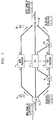
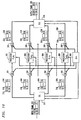
- FIG. 1 An example of this arrangement is shown in FIG. 1.
- the delay through the arrangement becomes consistent with the processing time for the slower processor 11 to process a unit of data, the first data block 16.
- the faster processor 12 starts processing after the proportionate number of data blocks 16 have arrived to be processed by the slower processor 11.
- the entire process repeats indefinitely.
- the average throughput is shown in FIG. 3 to be equal the weighted average throughput of processors 11 and 12 and their relative processing rates.
- the input gating functions (I.G.) 17 and output gating function (O.G.) 18 also get simplified in this case.
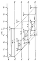
- the timing diagram for the arrangement of FIG. 1 is shown in FIG. 2.
- the top time line in FIG. 2 shows the arrival times of data blocks 16.
- Each of the subsequent time lines shows the progression of individual data blocks 16 of a frame 15 through the arrangement of FIG. 1.
- the gating function 17 that is applied to the input data blocks 16 follows a simple rule.
- the slower processor 11 receives the first block 16 and starts processing immediately.
- the faster processor 12 must wait for the second block 16 and starts processing immediately.
- the third and fourth blocks 16 are collected in input buffer (I.B.) 19 as they arrive, and processor 12 processes the blocks 16 one after another continuously.
- the end of the processing of the first block 16 coincides with the arrival of the first block 16 of the next repetitive input frame 15, while the end of processing of the fourth block 16 coincides with the arrival of the second block 16 of this next repetitive input frame 15.
- the processed first input block 16 forms the first output data block (O.D.) 26, and is gated out by gating function 18 immediately.
- CLK. common clock
- the required clock rates are derived by applying frequency dividers (e.g., counters) to the common clock 21 rate.
- the number of processors can be increased to any number m, provided that the number of blocks 16 processed by each processor is in direct proportion to its processing rate vis-a-vis the processing rates of the other processors.
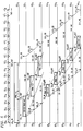
- the slowest processor 111 requires 9t seconds to process one data block 116, with t seconds being the inter-arrival time of each block 116.
- the second and third processors 112 and 113 require 3t and 1.8t, respectively, to process each data blocks 116.
- the throughput of the system is one block 116 per t seconds, being faster than the fastest processor 113 rate and equal to the inter-arrival time for each data block 116.
- Input blocks 116 are distributed to processors 111, 112, and 113 by an input gating function 117, and are processed to form corresponding output blocks 126 which are assembled at an output gating function 118 into an output frame 125 that duplicates input frame 115 in the ordering of processor input blocks 116.
- No memory is required in the system other than the temporary input and output storage buffers 119, 120, 139, and 140, whose operation is in synchronism with the process times.
- the processors 111, 112, and 113 are never idle and function synchronously.
- the timing diagram for the arrangement of FIG. 4 is shown in FIG. 5. The requisite relations that ascertain that all three processors 111, 112, and 113 will never be idle are presented in FIG. 6.
- the structure can be extended to m processors with any integer relation between the processor clock rates.
- any segment of the parallel arrangements shown in the earlier configurations can be dropped without any loss of generality. This leads to any generalized number of parallel processor paths and any relation between their rates. For example, if the slow processor 111 of FIG. 4 is dropped, the two processors 112 and 113 with a 3:5 proportioning between their rates will function properly if the number of input data blocks per input data frame is made eight instead of nine, as discussed next in this section. This configuration is shown in FIG. 7
- the slower clock is derived from a binary counter of the faster clock.
- modulo-i counters become necessary for any integer, i, relation between the clock rates of Sections 4.1 and 4.2.
- bit-slicing to rate equaling the least common multiple of the two rates, becomes necessary.
- FIG. 10 shows any number of processors 300, having any operating characteristics, connected in parallel, each being served at its input by an associated input buffer 301 and at its output by an associated output buffer 302.
- the input buffers 301 are connected to a common input point through an input gating function 317, and the output buffers 302 are connected to a common output point through an output gating function 318.
- the input gating function 317 distributes to the processors 300 sets of data blocks 316 of input frames 315.
- Each processor 300 processes the received data blocks 316 into output data blocks 326, which are gathered and assembled by the output gating function 318 into output frames 325.
- FIG. 11 shows which data blocks 316 are processed by which processor 300 and how fast.
- the operations of all elements of FIG. 10 are synchronized by a common clock 303.
- any arbitrary segment of a computing network can be replaced by such an arrangement.
- the clock rates are adjusted properly, a data stream arriving at a uniform rate will pass through the newly-synthesized structure at the same rate andwith the same delay as it would through the segment that the structure has replaced.
- the processors will be 100 percent utilized 100 percent of the time. The timing considerations to effect this result are shown in FIG. 12.
- the throughput of the structure will be faster than the throughput of the fastest single processor within that structure.
- the gating of various data blocks is simple and efficient. If the cost of the slower processors decreases at a rate faster than the clock rate, the structures proposed here will be cheaper than the higher-priced single-processor systems of the same speed. Alternatively, if the slower processors operate more dependably than the faster processors, then the system performance of the proposed configuration will be more dependable.
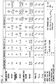
- FIG. 10 depicts a generalized processor structure to process N-block 316 frames 315 of data.
- Data arrives uniformly at one block 316 per t seconds into a network with k processors 300 operating in parallel.
- the slowest processor P 1 processes a 1 blocks 316 of data in T seconds
- the fastest processor P k processes a k blocks 316 of data in the same duration of T seconds.
- the i-th processor 300 clocking at T/a i rate per data block 316, will process data blocks m.. (n-1), and the i - th input and output buffers 301 and 302 will hold the same (unprocessed and processed, respectively,) data blocks, where
- the flow of a i blocks 316 of data in the i-th parallel branch of the configuration follows the duration and timing pattern presented in FIG. 12.
- the second column indicates the timing of the m-th block 316 as it is processed in the i-th processor branch of the architectural arrangement in FIG. 10.
- This block 316 enters the processor 300 upon arrival (with zero wait-time in the input buffer) for N/a i seconds, and then exists to the output buffer 301 as a processed data block. Here it waits for (D-N ⁇ t/a i ) seconds, starting from an instant (m+N/a i ) ⁇ t seconds to (D+m ⁇ t) seconds. At this time it exits out of the processor branch as an output data block 326.
- the (m+1)st data block 316 follows the timing durations and instants in the third column, and so on. It is interesting to note the linear increase of the durations of data in the input buffer 301 for each consecutive data block 316, as shown by row one of FIG. 12.
- the processing time for each block 316 remains the same, at N ⁇ t/a i seconds.
- the processed data blocks leave the processor 300 at an interval of one block per t seconds, which corresponds to the arrival time of each block 316, after an overall system delay of D seconds.
- the basic units described in Section 4 above, and illustrated in FIGS. 1, 4, 7, and 10, become the building blocks in the pipeline.
- the pipeline can be visualized as a chain of various production stages in which the completion time of all of the stages is uniform.
- Multiple processors of varying rates can be freely used to construct any or each production stage in the pipeline. For example, if a conventional pipeline 400 has four stages 401, 402, 403, and 404, as shown in FIG. 13, then each of the stages needs the same finite amount of time for execution. That way, each one of the stages of the pipeline is continuously busy, with data blocks following in the 401, 402, 403, and 404 sequence through the pipeline 400.
- any arbitrary segment of a computing network can be replaced by a series, parallel, or series/parallel processor arrangement.
- this relieves the burden on the VLSI chip manufacturers, who are generally not able to sustain a high yield on very fast chips.
- SIMD single-instruction, multiple-data arrangement
- MIMD multiple-instruction, multiple-data arrangement
- the unified control may be shared from a single control unit and data may be channeled from a memory bank.
- the flow of data to and from the processors needs appropriate buffering and gating as discussed in Section 4.
- Control (or the opcode of the instruction) to each processor flows only once. In this case, the completion time for processors may be accurately sliced, and thus the data flow in and out of the various processors can be accurately synchronized. This synchronized operation is used to ascertain 100 percent processor utilization.
- the flow of programs and data from disk to memory needs to be gated and stored in active memory, such that independent processors of varying speeds may coexist.
- the processors that share in this environment might not be as algorithmically related as suggested in Section 4; however, if the faster processors handle longer tasks for the same amount of time, and vice versa, then the average delay for the job completion time can be maintained for short and long jobs. Further, the probability of taxing the DMA channels between disk and memory is reduced, since the average input and output rates in and out of the system follow a somewhat uniform rate.
- the operating system routines may already follow a job allocation strategy if processors of different rates coexist.
- the architecture presented in this discussion streamlines the job flow, if processor rates and processor allocations are coordinated with the expected duration for job completion.
- a set of processors operating in parallel need not be synchronized by being clocked by signals derived from a single common clock; instead, each may have its own clock and only the clocks need be synchronized with each other.
- the individual processors may take the reduced form of individual CPUs or even ALUs, depending upon system configuration.
- the gating functions can take any one of a variety of forms, such as simple conductor junctures, or simple logic gates on bus data leads.
- the input gating function may exist only in virtual form, its functionality being assumed by a source of the input data that addresses the processors individually and sends data at any one time only to the addressed processor.
- the output gating function of a stage may be combined with, and also serve as, the input gating function of the next stage.
- the invention may advantageously be applied to neural computing networks, such as may be used for image processing of satellite surveillance or medical image data.
Landscapes
- Engineering & Computer Science (AREA)
- Software Systems (AREA)
- Theoretical Computer Science (AREA)
- Physics & Mathematics (AREA)
- General Engineering & Computer Science (AREA)
- General Physics & Mathematics (AREA)
- Multi Processors (AREA)
Claims (12)
- Multiprozessorsystem umfassend:
eine Vielzahl von parallel arbeitenden Prozessoren (11, 12; 111 - 113; 300), wobei jeder Prozessor von wenigstens einigen der Prozessoren eine Aufgabe (15; 115; 215; 315) mit einer anderen Geschwindigkeit (langsam, schnell; langsam, mittel, schnell) abwickelt, so daß jeder dieser Prozessoren die Aufgabe in einer anderen Zeitdauer als die anderen Prozessoren abwickelt,
gekennzeichnet durchdie Vielzahl von Prozessoren, die alle synchron miteinander arbeiten (21; 121; 221; 303), wobeidas System ferner aufweist:eine erste Einrichtung (17; 117; 217; 317), die mit der Vielzahl von Prozessoren verbunden ist, um eine Aufgabe, die eine Folge (I.D.O - I.D.n-1) von mehreren Unteraufgaben (16; 116; 216; 316) umfaßt, zu empfangen und Teile der empfangenen Aufgabe an einzelne Prozessoren zum Abwickeln zu verteilen, wobei jeder Teil mindestens eine Unteraufgabe umfaßt und die Unteraufgaben jedes Teils in der Folge aufeinanderfolgen, wobei die Teile in ihrer Größe unmittelbar proportional zu den Arbeitsgeschwindigkeiten der einzelnen Prozessoren sind, so daß jeder einzelne Prozessor den ihm zugeteilten Teil der Aufgabe in der gleichen Zeitdauer abwickelt, wie die anderen Prozessoren die ihnen zugeteilten Teile abwickeln, wobei die erste Einrichtung aufeinanderfolgende Teile an die Vielzahl der Prozessoren in umgekehrter Reihenfolge der Arbeitsgeschwindigkeiten der Prozessoren derart verteilt, daß der Prozessor mit der niedrigsten Arbeitsgeschwindigkeit den ersten Teil der aufeinanderfolgenden Teile und der Prozessor mit der höchsten Arbeitsgeschwindigkeit den letzten Teil der aufeinanderfolgenden Teile erhält; undeine zweite Einrichtungen (18; 118; 218; 318), die mit der Vielzahl der Prozessoren zur Ausgabe der Abwicklungsergebnisse verbunden ist. - Multiprozessorsystem nach Anspruch 1, wobei die zweite Einrichtung folgendes Merkmal umfasst:eine Einrichtung (20; 120; 140; 220; 240) zum Empfangen der Abwicklungsergebnisse von der Vielzahl der Prozessoren und Zusammenfügen der Ergebnisse zu einem gemeinsamen Ausgangssignal (18; 118; 218; 318), wobei die Ergebnisse von der Vielzahl der Prozessoren in der gleichen Reihenfolge aufeinanderfolgend zusammengefügt werden, in der die Teile, die sich aus den entsprechenden Ergebnissen ergaben, von der ersten Einrichtung empfangen worden sind.
- Multiprozessorsystem nach Anspruch 2 mit folgenden weiteren Merkmalen:eine Eingangspuffereinrichtung (19; 119; 139; 219; 239; 301), die mit der ersten Einrichtung und mit einzelnen Prozessoren der Vielzahl von Prozessoren verbunden ist, und synchron mit den angeschalteten Prozessoren arbeitet, zum sequentiellen und seriellen Empfangen von Unteraufgaben der einzelnen Aufgabenteile mit einer gleichmäßigen Geschwindigkeit, zum Speichern der Aufgabenteile, die von der ersten Einrichtung an die angeschalteten Prozessoren verteilt werden, und zum Eingeben der gespeicherten Aufgabenteile in die angeschalteten Prozessoren mit einer Geschwindigkeit, die mit den Arbeitsgeschwindigkeiten der angeschalteten Prozessoren derart synchronisiert sind, daß jede Eingangspuffereinrichtung seinem einzelnen Prozessor eine Unteraufgabe eines Teils zuführt, die dem einzelnen Prozessor umgehend zugeführt wird, wenn dieser das Abwickeln einer Unteraufgabe beendet, die zuletzt dem einzelnen Prozessor zugeführt worden ist; undeine Ausgangspuffereinrichtung (20; 120, 140; 220; 240; 302), die mit einzelnen der Vielzahl von Prozessoren und der zweiten Einrichtung und mit der Vielzahl der Prozessoren synchron arbeitet, zum Empfangen der Abwicklungsergebnisse jeder Unteraufgabe der Teile, die zu den angeschalteten Prozessoren umgehend zugeführt werden, wenn die angeschalteten Prozessoren die Abwicklung jeder Unteraufgabe beendet und die Abwicklungsergebnisse gespeichert haben, und zur Ausgabe der gespeicherten Ergebnisse zu Zeiten und mit Geschwindigkeiten, die mit den Arbeitsgeschwindigkeiten der Vielzahl der Prozessoren derart synchronisiert sind, daß jede Ausgangspuffereinrichtung die Abwicklungsergebnisse der Unteraufgaben der einzelnen Aufgabenteile mit der gleichmäßigen Geschwindigkeit ausgibt, mit welcher jede entsprechende Eingangspuffereinrichtung die Unteraufgaben der einzelnen Aufgabenteile empfängt.
- Multiprozessorsystem nach Anspruch 2, dadurch gekennzeichnet, daßdie an die Vielzahl von Prozessoren verteilte Aufgabe einen ersten Datenstrom umfaßt, der von der ersten Einrichtung mit einer gleichmäßigen Geschwindigkeit empfangen wird, wobei die gleichmäßige Geschwindigkeit eine kombinierte Geschwindigkeit ist, mit der die Daten durch die Vielzahl der Prozessoren verarbeitet werden; daß die Verarbeitungsergebnisse verarbeitete Daten umfassen; und daßdas gemeinsame Ausgangssignal einen zweiten Strom der verarbeiteten Daten umfasst, die von der zweiten Einrichtung mit einer gleichmäßigen Geschwindigkeit ausgegeben werden.
- Multiprozessorsystem nach Anspruch 4, dadurch gekennzeichnet, daßder erste Datenstrom eine Folge von ersten Datenrahmen umfaßt, die jeweils eine identische Menge an Dateneinheiten enthalten; daßdie erste Einrichtung eine unterschiedliche Menge an Dateneinheiten aus jedem ersten Rahmen jedem Prozessor zur Verarbeitung zuführt, wobei die Mengen aus jedem ersten Rahmen, die den verschiedenen Prozessoren zugeführt werden, im gleichen Verhältnis stehen wie die Arbeitsgeschwindigkeiten der Prozessoren; und daßdie zweite Einrichtung die verarbeiteten Daten, die von den Prozessoren erhalten werden, zu einer Folge von zweiten Datenrahmen zusammenfügt, die jeweils eine identische Menge an verarbeiteten Daten enthalten und jeweils eine unterschiedliche Menge an verarbeiteten Daten von jedem der Prozessoren erhalten, wobei die von den verschiedenen Prozessoren erhaltenen Mengen, die in jedem zweiten Rahmen enthalten sind, im gleichen Verhältnis stehen wie die Arbeitsgeschwindigkeiten der Prozessoren.
- Multiprozessorsystem nach Anspruch 4, dadurch gekennzeichnet, daßdas Multiprozessorsystem eine Vielzahl von kaskadierten Verarbeitungsstufen (401 - 404; 1401 - 1404) umfaßt, die jeweils Daten mit der gleichen Geschwindigkeit verarbeiten können, so daß jede Stufe eine Dateneinheit in der gleichen Zeitperiode wie die anderen Stufen verarbeiten kann, und die jeweils synchron miteinander arbeiten, wobei wenigstens eine der Stufen die Vielzahl der Prozessoren umfaßt; daßdie erste Einrichtung zum Empfangen des ersten Datenstroms von außerhalb der Stufen dient; und daß die zweite Einrichtung zur Ausgabe des zweiten Datenstromes aus der Stufe dient.
- Multiprozessorsystem nach Anspruch 6, dadurch gekennzeichnet, daßder erste Datenstrom eine Folge von ersten Datenrahmen umfaßt, die jeweils eine identische Menge an Dateneinheiten enthalten, daßdie erste Einrichtung eine unterschiedliche Menge an Dateneinheiten von jedem ersten Rahmen jedem Prozessor wenigstens einer der Stufen zur Verarbeitung zuführt, wobei die Mengen von jedem ersten Rahmen, die an verschiedene Prozessoren verteilt werden, im gleichen Verhältnis wie die Arbeitsgeschwindigkeiten der Prozessoren stehen; und daßdie zweite Einrichtung die von den Prozessoren wenigstens einer der Stufen erhaltenen, verarbeiteten Daten zu einer Folge von zweiten Datenrahmen zusammenfügt, die jeweils eine identische Menge an verarbeiteten Daten und eine unterschiedliche Menge an verarbeiteten Daten enthalten, die von jedem Prozessor kommen, wobei die in jedem zweiten Rahmen enthaltenen Mengen, die von verschiedenen Prozessoren kommen, im gleichen Verhältnis wie die Arbeitsgeschwindigkeiten der Prozessoren stehen.
- Verfahren zum Betreiben eines Multiprozessorsystems, umfassend eine Vielzahl von Prozessoren (11, 12; 111 - 113; 300), die parallel arbeiten, wobei jeder Prozessor von wenigstens einigen der Prozessoren eine Aufgabe (15; 115; 215; 315) mit einer unterschiedlichen Geschwindigkeit (langsam, schnell, langsam, mittel, schnell) verarbeiten kann, so daß jeder Prozessor von wenigstens einigen der Prozessoren die Aufgabe während einer anderen Zeitdauer als die anderen Prozessoren abwickelt, gekennzeichnet durch eine Vielzahl von Prozessoren, die sämtlich synchron miteinander arbeiten (21; 121; 221; 303), wobei das Verfahren die Schritte umfaßt:Empfangen einer Aufgabe, die eine Folge (I.D.0 - I.D.n-1) von mehreren Unteraufgaben (16; 116; 216; 316) umfaßt;Zuführen (17; 117; 217; 317) von Teilen der empfangenen Aufgabe zu einzelnen Prozessoren zur Verarbeitung, wobei jeder Teil wenigstens eine Unteraufgabe umfaßt und die Unteraufgaben von jedem Teil in der Folge aufeinanderfolgen, wobei die Teile in ihrer Größe unmittelbar proportional zu den Arbeitsgeschwindigkeiten der einzelnen Prozessoren sind und die aufeinanderfolgenden Teile an die Vielzahl von Prozessoren in umgekehrter Reihenfolge zu den Arbeitsgeschwindigkeiten der Prozessoren derart geliefert werden, daß der Prozessor mit der niedrigsten Geschwindigkeit den ersten Teil der aufeinanderfolgenden Teile und der Prozessor mit der höchsten Geschwindigkeit den letzten Teil der aufeinanderfolgenden Teile erhält;Verarbeiten (11, 12; 111 - 113; 300) des in jedem Prozessor empfangenen Teils mit der Geschwindigkeit des empfangenden Prozessors, so daß jeder einzelne Prozessor den ihm zugeführten Teil der Aufgabe in der gleichen Zeitdauer verarbeitet, in der die anderen Prozessoren die an sie verteilten Teile verarbeiten; undAusgabe (18; 118, 218; 318) der Verarbeitungsergebnisse.
- Verfahren nach Anspruch 8, wobei der Verfahrensschritt der Ausgabe die Schritte umfaßt:Erhalten der Verarbeitungsergebnisse von der Vielzahl der Prozessoren; undaufeinanderfolgendes Zusammenfügen der Ergebnisse, die von der Vielzahl der Prozessoren erhalten worden sind, zu einem gemeinsamen Ausgangssignal, und zwar in der gleichen Reihenfolge, in der die Teile, die sich aus den entsprechenden Ergebnissen ergaben, in der empfangenen Aufgabe angeordnet sind.
- Verfahren nach Anspruch 9, wobei das
Multiprozessorsystem ferner umfaßt:Eingangspuffer und Ausgangspuffer, die mit einzelnen der Vielzahl von Prozessoren verbunden sind und synchron mit den angeschalteten Prozessoren arbeiten, wobei dem Verarbeitungsschritt die weiteren Verfahrensschritte vorangehen:Sequentielles und serielles Empfangen von Unteraufgaben der einzelnen Aufgabenteilen mit einer gleichmäßigen Geschwindigkeit und Speichern der Aufgabenteile, die den angeschalteten Prozessoren zugeführt werden, in den Eingangspuffer, undEingeben der gespeicherten Aufgabenteile von den Eingangspuffern in die angeschalteten Prozessoren mit Geschwindigkeiten, die mit den Arbeitsgeschwindigkeiten der angeschalteten Prozessoren derart synchronisiert sind, daß eine Unteraufgabe eines Teiles, der einem einzelnen Prozessor zugeführt wird, umgehend in die einzelnen Prozessor eingegeben wird, wenn der einzelne Prozessor die Verarbeitung einer Unteraufgabe, die zuletzt in den einzelnen Prozessor eingegeben worden ist, beendet hat; und wobeider Verfahrensschritt des Empfangens von den Prozessoren die folgenden Verfahrensschritte aufweist:Empfangen der Verarbeitungsergebnisse jeder Unteraufgabe der Teile, die den angeschalteten Prozessoren umgehend zugeführt werden, wenn die angeschalteten Prozessoren die Verarbeitung jeder Unteraufgabe beendet und die Verarbeitungsergebnisse in den Ausgangspuffern gespeichert haben, undAusgeben der gespeicherten Ergebnisse zu Zeiten und mit Geschwindigkeiten, die mit den Arbeitsgeschwindigkeiten der Vielzahl der Prozessoren derart synchronisiert sind, daß die Verarbeitungsergebnisse der Unteraufgaben der einzelnen Aufgabenteile mit einer gleichmäßigen Geschwindigkeit ausgegeben werden, mit welcher die Unteraufgaben der einzelnen Aufgabenteile empfangen werden. - Verfahren nach Anspruch 9, wobei:der Verfahrensschritt des Empfangens einer Aufgabe den Verfahrensschritt des Empfangens eines ersten Datenstromes mit einer gleichmäßigen Geschwindigkeit umfaßt, wobei die gleichmäßige Geschwindigkeit eine zusammengefügte Geschwindigkeit zum Verarbeiten der Daten durch die Vielzahl der Prozessoren ist;der Verfahrensschritt des Empfangens der Verarbeitungsergebnisse den Verfahrensschritt des Empfangens der verarbeiteten Daten umfaßt; undder Verfahrensschritt der Ausgabe der Ergebnisse den Verfahrensschritt der Ausgabe eines zweiten Stroms von verarbeiteten Daten mit einer gleichmäßigen Geschwindigkeit umfaßt.
- Verfahren nach Anspruch 11, wobeider Verfahrensschritt des Empfangens eines ersten Datenstroms den Verfahrensschritt des Empfangens eines ersten Datenstroms enthält, der eine Folge von ersten Datenrahmen umfaßt, die jeweils eine gleiche Menge an Dateneinheiten enthalten;der Verfahrensschritt des Zuführens den Verfahrensschritt des Zuführens einer unterschiedlichen Menge an Dateneinheiten aus jedem ersten Rahmen zu jedem Prozessor zur Verarbeitung umfaßt, wobei die Menge aus jedem ersten Rahmen, die verschiedenen Prozessoren zugeführt wird, im gleichen Verhältnis steht wie die Arbeitsgeschwindigkeiten der Prozessoren; undder Verfahrensschritt des Zusammenfügens den Verfahrensschritt des Zusammenfügens der verarbeiteten Daten, die vom Prozessor kommen, zu einer Folge von zweiten Datenrahmen enthält, welche jeweils die gleiche Menge an verarbeiteten Daten und eine unterschiedliche Menge an verarbeiteten Daten, die von jedem Prozessor kommen, enthalten, wobei die in jedem zweiten Rahmen enthaltenen Datenmengen, die von verschiedenen Prozessoren kommen, im gleichen Verhältnis stehen wie die Arbeitsgeschwindigkeiten der Prozessoren.
Applications Claiming Priority (2)
| Application Number | Priority Date | Filing Date | Title |
|---|---|---|---|
| US666162 | 1991-03-07 | ||
| US07/666,162 US5978831A (en) | 1991-03-07 | 1991-03-07 | Synchronous multiprocessor using tasks directly proportional in size to the individual processors rates |
Publications (3)
| Publication Number | Publication Date |
|---|---|
| EP0502680A2 EP0502680A2 (de) | 1992-09-09 |
| EP0502680A3 EP0502680A3 (en) | 1993-11-24 |
| EP0502680B1 true EP0502680B1 (de) | 1999-05-26 |
Family
ID=24673076
Family Applications (1)
| Application Number | Title | Priority Date | Filing Date |
|---|---|---|---|
| EP92301775A Expired - Lifetime EP0502680B1 (de) | 1991-03-07 | 1992-03-02 | Multiprozessor mit effizienter Verwendung von Prozessoren mit unterschiedlichen Leistungseigenschaften |
Country Status (4)
| Country | Link |
|---|---|
| US (1) | US5978831A (de) |
| EP (1) | EP0502680B1 (de) |
| JP (1) | JP2513960B2 (de) |
| DE (1) | DE69229244T2 (de) |
Families Citing this family (45)
| Publication number | Priority date | Publication date | Assignee | Title |
|---|---|---|---|---|
| JP3518034B2 (ja) * | 1995-03-30 | 2004-04-12 | 三菱電機株式会社 | ソート方法並びにソート処理装置並びにデータ処理装置 |
| JP3780732B2 (ja) * | 1999-03-10 | 2006-05-31 | 株式会社日立製作所 | 分散制御システム |
| EP1113575B1 (de) * | 1999-12-24 | 2006-04-05 | Matsushita Electric Industrial Co., Ltd. | Signalverarbeitungsvorrichtung und Verfahren |
| US6611920B1 (en) * | 2000-01-21 | 2003-08-26 | Intel Corporation | Clock distribution system for selectively enabling clock signals to portions of a pipelined circuit |
| JP3504210B2 (ja) * | 2000-03-31 | 2004-03-08 | 理想科学工業株式会社 | 画像処理装置 |
| WO2001078337A1 (en) * | 2000-04-11 | 2001-10-18 | Parthus Technologies Plc | Method and apparatus for multi-lane communication channel with deskewing capability |
| DE10059026A1 (de) * | 2000-11-28 | 2002-06-13 | Infineon Technologies Ag | Einheit zur Verteilung und Verarbeitung von Datenpaketen |
| GB2372847B (en) * | 2001-02-19 | 2004-12-29 | Imagination Tech Ltd | Control of priority and instruction rates on a multithreaded processor |
| JP4310926B2 (ja) * | 2001-02-26 | 2009-08-12 | 沖電気工業株式会社 | エコーキャンセラ装置 |
| US7233998B2 (en) * | 2001-03-22 | 2007-06-19 | Sony Computer Entertainment Inc. | Computer architecture and software cells for broadband networks |
| US7203943B2 (en) * | 2001-10-31 | 2007-04-10 | Avaya Technology Corp. | Dynamic allocation of processing tasks using variable performance hardware platforms |
| US7103628B2 (en) * | 2002-06-20 | 2006-09-05 | Jp Morgan Chase & Co. | System and method for dividing computations |
| US7640547B2 (en) * | 2002-02-08 | 2009-12-29 | Jpmorgan Chase & Co. | System and method for allocating computing resources of a distributed computing system |
| US7376693B2 (en) * | 2002-02-08 | 2008-05-20 | Jp Morgan Chase & Company | System architecture for distributed computing and method of using the system |
| US7380151B1 (en) * | 2002-12-11 | 2008-05-27 | National Semiconductor Corporation | Apparatus and method for asynchronously clocking the processing of a wireless communication signal by multiple processors |
| US7016695B1 (en) | 2002-12-11 | 2006-03-21 | National Semiconductor Corporation | Apparatus and method for processing a deterministic data flow associated with a wireless communication signal |
| US7296269B2 (en) * | 2003-04-22 | 2007-11-13 | Lucent Technologies Inc. | Balancing loads among computing nodes where no task distributor servers all nodes and at least one node is served by two or more task distributors |
| US20050021779A1 (en) * | 2003-04-29 | 2005-01-27 | Ahamed Syed V. | Localized knowledge-based intelligent network |
| US7478390B2 (en) * | 2003-09-25 | 2009-01-13 | International Business Machines Corporation | Task queue management of virtual devices using a plurality of processors |
| US7516456B2 (en) | 2003-09-25 | 2009-04-07 | International Business Machines Corporation | Asymmetric heterogeneous multi-threaded operating system |
| US7444632B2 (en) * | 2003-09-25 | 2008-10-28 | International Business Machines Corporation | Balancing computational load across a plurality of processors |
| US7496917B2 (en) * | 2003-09-25 | 2009-02-24 | International Business Machines Corporation | Virtual devices using a pluarlity of processors |
| US7475257B2 (en) | 2003-09-25 | 2009-01-06 | International Business Machines Corporation | System and method for selecting and using a signal processor in a multiprocessor system to operate as a security for encryption/decryption of data |
| US7549145B2 (en) | 2003-09-25 | 2009-06-16 | International Business Machines Corporation | Processor dedicated code handling in a multi-processor environment |
| US7318218B2 (en) * | 2003-09-25 | 2008-01-08 | International Business Machines Corporation | System and method for processor thread for software debugging |
| US7415703B2 (en) * | 2003-09-25 | 2008-08-19 | International Business Machines Corporation | Loading software on a plurality of processors |
| US20050071578A1 (en) * | 2003-09-25 | 2005-03-31 | International Business Machines Corporation | System and method for manipulating data with a plurality of processors |
| US7523157B2 (en) | 2003-09-25 | 2009-04-21 | International Business Machines Corporation | Managing a plurality of processors as devices |
| US7146529B2 (en) * | 2003-09-25 | 2006-12-05 | International Business Machines Corporation | System and method for processor thread acting as a system service processor |
| US7389508B2 (en) * | 2003-09-25 | 2008-06-17 | International Business Machines Corporation | System and method for grouping processors and assigning shared memory space to a group in heterogeneous computer environment |
| US7236998B2 (en) * | 2003-09-25 | 2007-06-26 | International Business Machines Corporation | System and method for solving a large system of dense linear equations |
| US20050071828A1 (en) * | 2003-09-25 | 2005-03-31 | International Business Machines Corporation | System and method for compiling source code for multi-processor environments |
| US20050080999A1 (en) * | 2003-10-08 | 2005-04-14 | Fredrik Angsmark | Memory interface for systems with multiple processors and one memory system |
| TW200717246A (en) * | 2005-06-24 | 2007-05-01 | Koninkl Philips Electronics Nv | Self-synchronizing data streaming between address-based producer and consumer circuits |
| US20060294401A1 (en) * | 2005-06-24 | 2006-12-28 | Dell Products L.P. | Power management of multiple processors |
| US7694107B2 (en) * | 2005-08-18 | 2010-04-06 | Hewlett-Packard Development Company, L.P. | Dynamic performance ratio proportionate distribution of threads with evenly divided workload by homogeneous algorithm to heterogeneous computing units |
| US20070094435A1 (en) * | 2005-10-25 | 2007-04-26 | Fry Walter G | Computer docking system and method |
| KR101224165B1 (ko) * | 2008-01-02 | 2013-01-18 | 삼성전자주식회사 | 데이터 처리 모듈 제어 방법 및 장치 |
| CN101677384B (zh) * | 2008-09-19 | 2011-03-23 | 鸿富锦精密工业(深圳)有限公司 | 数据存储管理系统及方法 |
| JP5258506B2 (ja) * | 2008-10-24 | 2013-08-07 | キヤノン株式会社 | 情報処理装置 |
| JP5017410B2 (ja) * | 2010-03-26 | 2012-09-05 | 株式会社東芝 | ソフトウェア変換プログラム、および、計算機システム |
| US8983632B2 (en) * | 2011-03-29 | 2015-03-17 | Honeywell International Inc. | Function block execution framework |
| US9684546B2 (en) * | 2014-12-16 | 2017-06-20 | Microsoft Technology Licensing, Llc | Job scheduling and monitoring in a distributed computing environment |
| US10530823B2 (en) * | 2016-08-10 | 2020-01-07 | At&T Intellectual Property I, L.P. | Network stream processing to ensuring a guarantee that each record is accounted for exactly once |
| CN112165572A (zh) * | 2020-09-10 | 2021-01-01 | Oppo(重庆)智能科技有限公司 | 图像处理方法、装置、终端及存储介质 |
Family Cites Families (29)
| Publication number | Priority date | Publication date | Assignee | Title |
|---|---|---|---|---|
| US3781822A (en) * | 1972-08-09 | 1973-12-25 | Bell Telephone Labor Inc | Data rate-changing and reordering circuits |
| US4251861A (en) * | 1978-10-27 | 1981-02-17 | Mago Gyula A | Cellular network of processors |
| US4316061A (en) * | 1979-11-23 | 1982-02-16 | Ahamed Syed V | Minimal delay rate-change circuits |
| US4312069A (en) * | 1980-02-07 | 1982-01-19 | Bell Telephone Laboratories, Incorporated | Serial encoding-decoding for cyclic block codes |
| US4495570A (en) * | 1981-01-14 | 1985-01-22 | Hitachi, Ltd. | Processing request allocator for assignment of loads in a distributed processing system |
| US4403286A (en) * | 1981-03-06 | 1983-09-06 | International Business Machines Corporation | Balancing data-processing work loads |
| US4584643A (en) * | 1983-08-31 | 1986-04-22 | International Business Machines Corporation | Decentralized synchronization of clocks |
| US4589066A (en) * | 1984-05-31 | 1986-05-13 | General Electric Company | Fault tolerant, frame synchronization for multiple processor systems |
| JPS61114363A (ja) * | 1984-11-07 | 1986-06-02 | Hitachi Ltd | 計算機システム間ジヨブ転送方式 |
| US4855903A (en) * | 1984-12-20 | 1989-08-08 | State University Of New York | Topologically-distributed-memory multiprocessor computer |
| US5015884A (en) * | 1985-03-29 | 1991-05-14 | Advanced Micro Devices, Inc. | Multiple array high performance programmable logic device family |
| US4742252A (en) * | 1985-03-29 | 1988-05-03 | Advanced Micro Devices, Inc. | Multiple array customizable logic device |
| US5151623A (en) * | 1985-03-29 | 1992-09-29 | Advanced Micro Devices, Inc. | Programmable logic device with multiple, flexible asynchronous programmable logic blocks interconnected by a high speed switch matrix |
| US4754398A (en) * | 1985-06-28 | 1988-06-28 | Cray Research, Inc. | System for multiprocessor communication using local and common semaphore and information registers |
| US4811210A (en) * | 1985-11-27 | 1989-03-07 | Texas Instruments Incorporated | A plurality of optical crossbar switches and exchange switches for parallel processor computer |
| JP2533495B2 (ja) * | 1986-07-25 | 1996-09-11 | 株式会社日立製作所 | ワ−クスケジユ−リング方法及び装置 |
| US4860201A (en) * | 1986-09-02 | 1989-08-22 | The Trustees Of Columbia University In The City Of New York | Binary tree parallel processor |
| US4843540A (en) * | 1986-09-02 | 1989-06-27 | The Trustees Of Columbia University In The City Of New York | Parallel processing method |
| US4891787A (en) * | 1986-12-17 | 1990-01-02 | Massachusetts Institute Of Technology | Parallel processing system with processor array having SIMD/MIMD instruction processing |
| US4954948A (en) * | 1986-12-29 | 1990-09-04 | Motorola, Inc. | Microprocessor operating system for sequentially executing subtasks |
| US4866664A (en) * | 1987-03-09 | 1989-09-12 | Unisys Corporation | Intercomputer communication control apparatus & method |
| US4979097A (en) * | 1987-09-04 | 1990-12-18 | Digital Equipment Corporation | Method and apparatus for interconnecting busses in a multibus computer system |
| JPS6467676A (en) * | 1987-09-09 | 1989-03-14 | Hitachi Ltd | Parallel computer |
| US5179687A (en) * | 1987-09-26 | 1993-01-12 | Mitsubishi Denki Kabushiki Kaisha | Semiconductor memory device containing a cache and an operation method thereof |
| US5031089A (en) * | 1988-12-30 | 1991-07-09 | United States Of America As Represented By The Administrator, National Aeronautics And Space Administration | Dynamic resource allocation scheme for distributed heterogeneous computer systems |
| US5146540A (en) * | 1990-02-22 | 1992-09-08 | International Business Machines Corp. | Processor allocation method and apparatus for multiprocessor execution of a constraint satisfaction search |
| JPH05500124A (ja) * | 1990-05-30 | 1993-01-14 | アダプティブ・ソリューションズ・インコーポレーテッド | Simdアーキテクチャにおける並行演算/通信機構 |
| US5142470A (en) * | 1990-09-26 | 1992-08-25 | Honeywell Inc. | Method of maintaining synchronization of a free-running secondary processor |
| US5130984A (en) * | 1990-12-18 | 1992-07-14 | Bell Communications Research, Inc. | Large fault tolerant packet switch particularly suited for asynchronous transfer mode (ATM) communication |
-
1991
- 1991-03-07 US US07/666,162 patent/US5978831A/en not_active Expired - Lifetime
-
1992
- 1992-02-05 JP JP4047735A patent/JP2513960B2/ja not_active Expired - Fee Related
- 1992-03-02 DE DE69229244T patent/DE69229244T2/de not_active Expired - Fee Related
- 1992-03-02 EP EP92301775A patent/EP0502680B1/de not_active Expired - Lifetime
Also Published As
| Publication number | Publication date |
|---|---|
| JP2513960B2 (ja) | 1996-07-10 |
| US5978831A (en) | 1999-11-02 |
| JPH04319758A (ja) | 1992-11-10 |
| EP0502680A3 (en) | 1993-11-24 |
| DE69229244D1 (de) | 1999-07-01 |
| DE69229244T2 (de) | 2000-01-27 |
| EP0502680A2 (de) | 1992-09-09 |
Similar Documents
| Publication | Publication Date | Title |
|---|---|---|
| EP0502680B1 (de) | Multiprozessor mit effizienter Verwendung von Prozessoren mit unterschiedlichen Leistungseigenschaften | |
| US11106510B2 (en) | Synchronization with a host processor | |
| US4414624A (en) | Multiple-microcomputer processing | |
| US5404550A (en) | Method and apparatus for executing tasks by following a linked list of memory packets | |
| CN1618061B (zh) | 功能性流水线 | |
| Gupta et al. | System-level synthesis using re-programmable components | |
| US5367690A (en) | Multiprocessing system using indirect addressing to access respective local semaphore registers bits for setting the bit or branching if the bit is set | |
| US5379428A (en) | Hardware process scheduler and processor interrupter for parallel processing computer systems | |
| US6269440B1 (en) | Accelerating vector processing using plural sequencers to process multiple loop iterations simultaneously | |
| US5056000A (en) | Synchronized parallel processing with shared memory | |
| EP2441013B1 (de) | Multithread-prozessoranordnung mit gemeinsamen ressourcen | |
| GB2569844A (en) | Sending data off-chip | |
| JP2019079529A (ja) | マルチタイル処理アレイにおける同期化 | |
| JP2501419B2 (ja) | 多重プロセッサメモリシステム及びメモリ参照競合解決方法 | |
| WO1999026148A2 (en) | Serialized, race-free virtual barrier network and method | |
| RU2042193C1 (ru) | Вычислительная система | |
| US20190155328A1 (en) | Synchronization in a multi-tile processing array | |
| GB2580314A (en) | Exchange of data between processor modules | |
| KR20190044573A (ko) | 컴퓨터 프로세싱의 타이밍 제어 | |
| US20050278720A1 (en) | Distribution of operating system functions for increased data processing performance in a multi-processor architecture | |
| JPS63184841A (ja) | 相互に関連したタスクの実行を制御する方法 | |
| Mazzola et al. | Enabling efficient hybrid systolic computation in shared-L1-memory manycore clusters | |
| Kohútka | A new FPGA-based architecture of task scheduler with support of periodic real-time tasks | |
| US11940940B2 (en) | External exchange connectivity | |
| Kohútka | Scheduling periodic real-time tasks with inter-task synchronisation |
Legal Events
| Date | Code | Title | Description |
|---|---|---|---|
| PUAI | Public reference made under article 153(3) epc to a published international application that has entered the european phase |
Free format text: ORIGINAL CODE: 0009012 |
|
| AK | Designated contracting states |
Kind code of ref document: A2 Designated state(s): DE FR GB IT |
|
| PUAL | Search report despatched |
Free format text: ORIGINAL CODE: 0009013 |
|
| AK | Designated contracting states |
Kind code of ref document: A3 Designated state(s): DE FR GB IT |
|
| RAP3 | Party data changed (applicant data changed or rights of an application transferred) |
Owner name: AT&T CORP. |
|
| 17P | Request for examination filed |
Effective date: 19940512 |
|
| 17Q | First examination report despatched |
Effective date: 19970421 |
|
| GRAG | Despatch of communication of intention to grant |
Free format text: ORIGINAL CODE: EPIDOS AGRA |
|
| GRAG | Despatch of communication of intention to grant |
Free format text: ORIGINAL CODE: EPIDOS AGRA |
|
| GRAH | Despatch of communication of intention to grant a patent |
Free format text: ORIGINAL CODE: EPIDOS IGRA |
|
| GRAH | Despatch of communication of intention to grant a patent |
Free format text: ORIGINAL CODE: EPIDOS IGRA |
|
| GRAA | (expected) grant |
Free format text: ORIGINAL CODE: 0009210 |
|
| AK | Designated contracting states |
Kind code of ref document: B1 Designated state(s): DE FR GB IT |
|
| PG25 | Lapsed in a contracting state [announced via postgrant information from national office to epo] |
Ref country code: IT Free format text: LAPSE BECAUSE OF FAILURE TO SUBMIT A TRANSLATION OF THE DESCRIPTION OR TO PAY THE FEE WITHIN THE PRE;WARNING: LAPSES OF ITALIAN PATENTS WITH EFFECTIVE DATE BEFORE 2007 MAY HAVE OCCURRED AT ANY TIME BEFORE 2007. THE CORRECT EFFECTIVE DATE MAY BE DIFFERENT FROM THE ONE RECORDED.SCRIBED TIME-LIMIT Effective date: 19990526 |
|
| REF | Corresponds to: |
Ref document number: 69229244 Country of ref document: DE Date of ref document: 19990701 |
|
| ET | Fr: translation filed | ||
| PLBE | No opposition filed within time limit |
Free format text: ORIGINAL CODE: 0009261 |
|
| 26N | No opposition filed | ||
| REG | Reference to a national code |
Ref country code: GB Ref legal event code: IF02 |
|
| PGFP | Annual fee paid to national office [announced via postgrant information from national office to epo] |
Ref country code: DE Payment date: 20070222 Year of fee payment: 16 |
|
| PGFP | Annual fee paid to national office [announced via postgrant information from national office to epo] |
Ref country code: GB Payment date: 20070228 Year of fee payment: 16 |
|
| PGFP | Annual fee paid to national office [announced via postgrant information from national office to epo] |
Ref country code: FR Payment date: 20070308 Year of fee payment: 16 |
|
| GBPC | Gb: european patent ceased through non-payment of renewal fee |
Effective date: 20080302 |
|
| REG | Reference to a national code |
Ref country code: FR Ref legal event code: ST Effective date: 20081125 |
|
| PG25 | Lapsed in a contracting state [announced via postgrant information from national office to epo] |
Ref country code: DE Free format text: LAPSE BECAUSE OF NON-PAYMENT OF DUE FEES Effective date: 20081001 |
|
| PG25 | Lapsed in a contracting state [announced via postgrant information from national office to epo] |
Ref country code: FR Free format text: LAPSE BECAUSE OF NON-PAYMENT OF DUE FEES Effective date: 20080331 |
|
| PG25 | Lapsed in a contracting state [announced via postgrant information from national office to epo] |
Ref country code: GB Free format text: LAPSE BECAUSE OF NON-PAYMENT OF DUE FEES Effective date: 20080302 |