EP0498884B1 - Process for producing optical coatings including niobium oxide by dc in-line reactive sputtering - Google Patents
Process for producing optical coatings including niobium oxide by dc in-line reactive sputtering Download PDFInfo
- Publication number
- EP0498884B1 EP0498884B1 EP91918239A EP91918239A EP0498884B1 EP 0498884 B1 EP0498884 B1 EP 0498884B1 EP 91918239 A EP91918239 A EP 91918239A EP 91918239 A EP91918239 A EP 91918239A EP 0498884 B1 EP0498884 B1 EP 0498884B1
- Authority
- EP
- European Patent Office
- Prior art keywords
- layer
- niobium oxide
- layers
- wavelength
- refractive index
- Prior art date
- Legal status (The legal status is an assumption and is not a legal conclusion. Google has not performed a legal analysis and makes no representation as to the accuracy of the status listed.)
- Expired - Lifetime
Links
- 238000000576 coating method Methods 0.000 title claims abstract description 79
- URLJKFSTXLNXLG-UHFFFAOYSA-N niobium(5+);oxygen(2-) Chemical compound [O-2].[O-2].[O-2].[O-2].[O-2].[Nb+5].[Nb+5] URLJKFSTXLNXLG-UHFFFAOYSA-N 0.000 title claims abstract description 67
- 229910000484 niobium oxide Inorganic materials 0.000 title claims abstract description 63
- 230000003287 optical effect Effects 0.000 title claims abstract description 39
- 238000000034 method Methods 0.000 title claims description 29
- 238000005546 reactive sputtering Methods 0.000 title abstract description 15
- 239000011248 coating agent Substances 0.000 claims abstract description 53
- VYPSYNLAJGMNEJ-UHFFFAOYSA-N Silicium dioxide Chemical compound O=[Si]=O VYPSYNLAJGMNEJ-UHFFFAOYSA-N 0.000 claims description 38
- 239000000758 substrate Substances 0.000 claims description 28
- 238000004544 sputter deposition Methods 0.000 claims description 25
- 239000000377 silicon dioxide Substances 0.000 claims description 19
- 235000012239 silicon dioxide Nutrition 0.000 claims description 18
- 229910052751 metal Inorganic materials 0.000 claims description 16
- 239000002184 metal Substances 0.000 claims description 16
- 238000000151 deposition Methods 0.000 claims description 12
- 239000011521 glass Substances 0.000 claims description 9
- 229910052782 aluminium Inorganic materials 0.000 claims description 7
- XAGFODPZIPBFFR-UHFFFAOYSA-N aluminium Chemical compound [Al] XAGFODPZIPBFFR-UHFFFAOYSA-N 0.000 claims description 7
- 239000004411 aluminium Substances 0.000 claims 5
- 238000001755 magnetron sputter deposition Methods 0.000 claims 5
- GWEVSGVZZGPLCZ-UHFFFAOYSA-N Titan oxide Chemical compound O=[Ti]=O GWEVSGVZZGPLCZ-UHFFFAOYSA-N 0.000 description 73
- 239000004408 titanium dioxide Substances 0.000 description 33
- XLOMVQKBTHCTTD-UHFFFAOYSA-N Zinc monoxide Chemical compound [Zn]=O XLOMVQKBTHCTTD-UHFFFAOYSA-N 0.000 description 23
- 239000000463 material Substances 0.000 description 23
- 239000011787 zinc oxide Substances 0.000 description 11
- BQCADISMDOOEFD-UHFFFAOYSA-N Silver Chemical compound [Ag] BQCADISMDOOEFD-UHFFFAOYSA-N 0.000 description 10
- 229910052709 silver Inorganic materials 0.000 description 10
- 239000004332 silver Substances 0.000 description 10
- 238000001429 visible spectrum Methods 0.000 description 10
- 230000008021 deposition Effects 0.000 description 8
- 238000004519 manufacturing process Methods 0.000 description 7
- 230000005540 biological transmission Effects 0.000 description 6
- 238000002310 reflectometry Methods 0.000 description 6
- OGIDPMRJRNCKJF-UHFFFAOYSA-N titanium oxide Inorganic materials [Ti]=O OGIDPMRJRNCKJF-UHFFFAOYSA-N 0.000 description 6
- XOLBLPGZBRYERU-UHFFFAOYSA-N tin dioxide Chemical compound O=[Sn]=O XOLBLPGZBRYERU-UHFFFAOYSA-N 0.000 description 5
- XKRFYHLGVUSROY-UHFFFAOYSA-N Argon Chemical compound [Ar] XKRFYHLGVUSROY-UHFFFAOYSA-N 0.000 description 4
- 239000011435 rock Substances 0.000 description 4
- 229910001887 tin oxide Inorganic materials 0.000 description 4
- QVGXLLKOCUKJST-UHFFFAOYSA-N atomic oxygen Chemical compound [O] QVGXLLKOCUKJST-UHFFFAOYSA-N 0.000 description 3
- 239000006185 dispersion Substances 0.000 description 3
- 229910052758 niobium Inorganic materials 0.000 description 3
- 239000010955 niobium Substances 0.000 description 3
- GUCVJGMIXFAOAE-UHFFFAOYSA-N niobium atom Chemical compound [Nb] GUCVJGMIXFAOAE-UHFFFAOYSA-N 0.000 description 3
- 239000001301 oxygen Substances 0.000 description 3
- 229910052760 oxygen Inorganic materials 0.000 description 3
- 238000005299 abrasion Methods 0.000 description 2
- 229910052786 argon Inorganic materials 0.000 description 2
- 239000002019 doping agent Substances 0.000 description 2
- 239000007789 gas Substances 0.000 description 2
- 239000012535 impurity Substances 0.000 description 2
- ORUIBWPALBXDOA-UHFFFAOYSA-L magnesium fluoride Chemical compound [F-].[F-].[Mg+2] ORUIBWPALBXDOA-UHFFFAOYSA-L 0.000 description 2
- ZKATWMILCYLAPD-UHFFFAOYSA-N niobium pentoxide Inorganic materials O=[Nb](=O)O[Nb](=O)=O ZKATWMILCYLAPD-UHFFFAOYSA-N 0.000 description 2
- BPUBBGLMJRNUCC-UHFFFAOYSA-N oxygen(2-);tantalum(5+) Chemical compound [O-2].[O-2].[O-2].[O-2].[O-2].[Ta+5].[Ta+5] BPUBBGLMJRNUCC-UHFFFAOYSA-N 0.000 description 2
- RVTZCBVAJQQJTK-UHFFFAOYSA-N oxygen(2-);zirconium(4+) Chemical compound [O-2].[O-2].[Zr+4] RVTZCBVAJQQJTK-UHFFFAOYSA-N 0.000 description 2
- 229920003023 plastic Polymers 0.000 description 2
- 229910001928 zirconium oxide Inorganic materials 0.000 description 2
- 229920006384 Airco Polymers 0.000 description 1
- RYGMFSIKBFXOCR-UHFFFAOYSA-N Copper Chemical compound [Cu] RYGMFSIKBFXOCR-UHFFFAOYSA-N 0.000 description 1
- KRHYYFGTRYWZRS-UHFFFAOYSA-N Fluorane Chemical compound F KRHYYFGTRYWZRS-UHFFFAOYSA-N 0.000 description 1
- PXGOKWXKJXAPGV-UHFFFAOYSA-N Fluorine Chemical compound FF PXGOKWXKJXAPGV-UHFFFAOYSA-N 0.000 description 1
- ATJFFYVFTNAWJD-UHFFFAOYSA-N Tin Chemical compound [Sn] ATJFFYVFTNAWJD-UHFFFAOYSA-N 0.000 description 1
- HCHKCACWOHOZIP-UHFFFAOYSA-N Zinc Chemical compound [Zn] HCHKCACWOHOZIP-UHFFFAOYSA-N 0.000 description 1
- 230000003667 anti-reflective effect Effects 0.000 description 1
- 239000005328 architectural glass Substances 0.000 description 1
- 230000008033 biological extinction Effects 0.000 description 1
- 230000015572 biosynthetic process Effects 0.000 description 1
- 229910052802 copper Inorganic materials 0.000 description 1
- 239000010949 copper Substances 0.000 description 1
- 238000005137 deposition process Methods 0.000 description 1
- 239000003989 dielectric material Substances 0.000 description 1
- 238000005516 engineering process Methods 0.000 description 1
- 239000011737 fluorine Substances 0.000 description 1
- 229910052731 fluorine Inorganic materials 0.000 description 1
- PCHJSUWPFVWCPO-UHFFFAOYSA-N gold Chemical compound [Au] PCHJSUWPFVWCPO-UHFFFAOYSA-N 0.000 description 1
- 229910052737 gold Inorganic materials 0.000 description 1
- 239000010931 gold Substances 0.000 description 1
- 229910000040 hydrogen fluoride Inorganic materials 0.000 description 1
- 238000002329 infrared spectrum Methods 0.000 description 1
- 229910001635 magnesium fluoride Inorganic materials 0.000 description 1
- 238000005259 measurement Methods 0.000 description 1
- 229910044991 metal oxide Inorganic materials 0.000 description 1
- 150000004706 metal oxides Chemical class 0.000 description 1
- 239000000203 mixture Substances 0.000 description 1
- 231100000989 no adverse effect Toxicity 0.000 description 1
- 230000000704 physical effect Effects 0.000 description 1
- 230000005855 radiation Effects 0.000 description 1
- 230000003678 scratch resistant effect Effects 0.000 description 1
- 239000004065 semiconductor Substances 0.000 description 1
- 238000005477 sputtering target Methods 0.000 description 1
- 238000006467 substitution reaction Methods 0.000 description 1
- 229910001936 tantalum oxide Inorganic materials 0.000 description 1
- 229910052725 zinc Inorganic materials 0.000 description 1
- 239000011701 zinc Substances 0.000 description 1
Images

Classifications
-
- C—CHEMISTRY; METALLURGY
- C03—GLASS; MINERAL OR SLAG WOOL
- C03C—CHEMICAL COMPOSITION OF GLASSES, GLAZES OR VITREOUS ENAMELS; SURFACE TREATMENT OF GLASS; SURFACE TREATMENT OF FIBRES OR FILAMENTS MADE FROM GLASS, MINERALS OR SLAGS; JOINING GLASS TO GLASS OR OTHER MATERIALS
- C03C17/00—Surface treatment of glass, not in the form of fibres or filaments, by coating
- C03C17/34—Surface treatment of glass, not in the form of fibres or filaments, by coating with at least two coatings having different compositions
- C03C17/3411—Surface treatment of glass, not in the form of fibres or filaments, by coating with at least two coatings having different compositions with at least two coatings of inorganic materials
- C03C17/3417—Surface treatment of glass, not in the form of fibres or filaments, by coating with at least two coatings having different compositions with at least two coatings of inorganic materials all coatings being oxide coatings
-
- G—PHYSICS
- G02—OPTICS
- G02B—OPTICAL ELEMENTS, SYSTEMS OR APPARATUS
- G02B1/00—Optical elements characterised by the material of which they are made; Optical coatings for optical elements
- G02B1/10—Optical coatings produced by application to, or surface treatment of, optical elements
- G02B1/11—Anti-reflection coatings
- G02B1/113—Anti-reflection coatings using inorganic layer materials only
- G02B1/115—Multilayers
-
- Y—GENERAL TAGGING OF NEW TECHNOLOGICAL DEVELOPMENTS; GENERAL TAGGING OF CROSS-SECTIONAL TECHNOLOGIES SPANNING OVER SEVERAL SECTIONS OF THE IPC; TECHNICAL SUBJECTS COVERED BY FORMER USPC CROSS-REFERENCE ART COLLECTIONS [XRACs] AND DIGESTS
- Y10—TECHNICAL SUBJECTS COVERED BY FORMER USPC
- Y10S—TECHNICAL SUBJECTS COVERED BY FORMER USPC CROSS-REFERENCE ART COLLECTIONS [XRACs] AND DIGESTS
- Y10S428/00—Stock material or miscellaneous articles
- Y10S428/913—Material designed to be responsive to temperature, light, moisture
-
- Y—GENERAL TAGGING OF NEW TECHNOLOGICAL DEVELOPMENTS; GENERAL TAGGING OF CROSS-SECTIONAL TECHNOLOGIES SPANNING OVER SEVERAL SECTIONS OF THE IPC; TECHNICAL SUBJECTS COVERED BY FORMER USPC CROSS-REFERENCE ART COLLECTIONS [XRACs] AND DIGESTS
- Y10—TECHNICAL SUBJECTS COVERED BY FORMER USPC
- Y10T—TECHNICAL SUBJECTS COVERED BY FORMER US CLASSIFICATION
- Y10T428/00—Stock material or miscellaneous articles
- Y10T428/24—Structurally defined web or sheet [e.g., overall dimension, etc.]
- Y10T428/24942—Structurally defined web or sheet [e.g., overall dimension, etc.] including components having same physical characteristic in differing degree
-
- Y—GENERAL TAGGING OF NEW TECHNOLOGICAL DEVELOPMENTS; GENERAL TAGGING OF CROSS-SECTIONAL TECHNOLOGIES SPANNING OVER SEVERAL SECTIONS OF THE IPC; TECHNICAL SUBJECTS COVERED BY FORMER USPC CROSS-REFERENCE ART COLLECTIONS [XRACs] AND DIGESTS
- Y10—TECHNICAL SUBJECTS COVERED BY FORMER USPC
- Y10T—TECHNICAL SUBJECTS COVERED BY FORMER US CLASSIFICATION
- Y10T428/00—Stock material or miscellaneous articles
- Y10T428/24—Structurally defined web or sheet [e.g., overall dimension, etc.]
- Y10T428/24942—Structurally defined web or sheet [e.g., overall dimension, etc.] including components having same physical characteristic in differing degree
- Y10T428/2495—Thickness [relative or absolute]
- Y10T428/24967—Absolute thicknesses specified
- Y10T428/24975—No layer or component greater than 5 mils thick
Definitions
- the present invention relates generally to processes for producing multilayer optical coatings for transparent substrates, and more particularly to such processes wherein the layers are deposited by DC reactive sputtering.
- DC reactive sputtering is the process most often used for large area commercial coating applications.
- Metal oxide layers for example, are deposited by sputtering the appropriate metal in an atmosphere including oxygen.
- the articles to be coated are passed through a series of in-line vacuum chambers each including sputtering sources. The chambers are isolated from one another by vacuum locks. Such a system may be referred to as an in-line system or simply a glass coater.
- Multilayer antireflection coatings are made by depositing two or more layers of transparent dielectric materials on a substrate. At least one of the layers has a refractive index higher than that of the substrate on which the coating.
- the coatings may be designed to reduce reflection at all wavelengths in the visible spectrum. The coatings may yield reflection values less than 0.25 percent over the visible spectrum.
- the time it takes to deposit a coating is determined mainly by the number of layers and the sputtering rate of the materials.
- the use of a glass coater to deposit multilayer antireflection coatings can significantly reduce their cost and thus extend their range of application.
- Such coatings may be used on picture frame glass and a display case, and as thermal control coatings for architectural and automobile glazings.
- the first or outermost layer of the system has a refractive index lower than that of the substrate and an optical thickness of about one-quarter wavelength at a wavelength of about 520 nanometers (nm).
- the second or middle layer has a refractive index higher than that of the substrate, and an optical thickness of about one-half wavelength at a wavelength of about 520 nm.
- the third layer i . e . the layer deposited on the substrate, has a refractive index greater than that of the substrate but less than the refractive index of the second layer.
- the optical thickness of the third layer is about one-quarter wavelength at a wavelength of about 520 nm.
- a disadvantage of the basic three layer system is that the refractive indices of the layers must have specific values in order to produce the lowest reflectivity.
- the selection and control of the refractive index of the third layer is particularly important. Departure from specific values of refractive index can not be compensated for by varying the thicknesses of the layers.
- the Rock system includes four layers.
- the first or outermost layer has a refractive index lower than that of the substrate and an optical thickness of about one-quarter wavelength at a wavelength of about 520 nm.
- the second or middle layer has a refractive index higher than that of the substrate and an optical thickness of about one-half to sixth-tenths of a wavelength at a wavelength of about 520 nm.
- the third layer has a thickness of about one-tenth of a wavelength at a wavelength of about 520 nm.
- the refractive index of the third layer is less than that of the second layer.
- the fourth layer has an optical thickness of about one-tenth of a wavelength at a wavelength of about 520 nm, and a refractive index greater than that of the third layer and the substrate.
- the third layer may be the same material as the first layer and the fourth layer may be the same material as the second layer.
- the Rock system may be used with different combinations of materials. Differences in refractive indices may be compensated for by different layer thicknesses.
- Magnesium fluoride (MgF2) can be used to form the outer and third layers. If a higher refractive index material were used for the outer layer, then the refractive index of the second layer would also need to be higher to produce the lowest reflectivity.
- Magnesium fluoride may be deposited by sputtering but requires a reactive atmosphere including fluorine or hydrogen fluoride.
- the outer layer is usually silicon dioxide (SiO 2 ). Silicon dioxide has a refractive index of about 1.46 at a wavelength of about 520 nm. If the reactive index of the first layer is about 1.46, a second layer having a refractive index of about 2.35 would provide the lowest reflection over the visible spectrum. Titanium dioxide (TiO 2 ) has a refractive index of about 2.35 at a wavelength of about 520 nm. As such, it is commonly used as the high refractive index material in a system deposited by DC reactive sputtering.
- the Rock system may require approximately equal thicknesses of titanium dioxide and silicon dioxide. Silicon dioxide may be sputtered four times faster than titanium dioxide. In order to operate at optimum speed, a glass coater may require four times as many sputtering cathodes for titanium dioxide as for silicon dioxide. However, the coater may not have enough chambers to accommodate all of these titanium dioxide cathodes. Thus, the deposition rate for the silicon dioxide will have to be reduced to "keep pace" with the deposition rate of the titanium dioxide. This reduces output and increases production costs.
- tin oxide (SnO 2 ) zinc oxide (ZnO) may be deposited by DC reactive sputtering at a rate at least six times faster than that of titanium oxide. These materials, however, have a refractive index of about 1.9 at a wavelength of 520 nm. The photopic reflection of a four layer antireflection coating using zinc oxide or tin oxide as the second layer would only be about 0.4 percent.
- Highly-reflecting coatings include enhanced metal reflectors which have a metal layer overcoated with low and high refractive index materials.
- Enhanced reflectors may have four such overcoating layers, including two high and two low refractive index layers arranged alternately.
- the overcoating layers each have an optical thickness of about one-quarter wavelength at a wavelength of about 520 nm.
- a low refractive index layer is in contact with the metal layer.
- the refractive index of the high refractive index material should be as high as possible and the refractive index of the low refractive index material should be as low as possible. This provides optimum reflection enhancement.
- the high and low index materials should also not absorb visible light.
- low emissivity coatings In the architectural glass coating industry, zinc oxide is used as a layer material for the formation of low emissivity (E) coatings. These coatings are designed to reflect long wavelength infrared radiation while transmitting visible light. They also have a low reflection for visible light from at least one surface.
- a low E coating may comprise three layers, for example, a silver layer bounded by two dielectric layers. The silver layer must be thick enough to provide high infrared reflection. The dielectric layers reduce reflection from the silver layer in the visible spectrum and thus enhance light transmission through the coated glass. The silver layer is preferably between about 10 and 15 nm thick.
- the refractive index of the dielectric layers should be relatively high. A material with a refractive index of about 2.35 at a wavelength of about 520 nm, such as titanium dioxide, would be preferred over zinc oxide for the reflection-reducing layers.
- Zinc oxide has a refractive index of about 1.9 at a wavelength of about 520 nm.
- the higher index permits the use of a thicker silver layer while maintaining low visible light transmission and high reflection.
- a silver layer about 8 nm thick produces the lowest reflectivity.
- a silver layer about 130 nm thick produces the lowest reflectivity.
- the thicker silver layer may also provide higher reflection at longer wavelengths, i . e . a lower emissivity.
- the thicker silver layer may also provide a higher reflection and lower transmission in the near infrared spectrum, reducing the solar heat load.
- the industry preference for zinc oxide is substantially based on its high sputtering rate. The lower production costs afforded by the high sputtering rate may be sufficient to justify the less than optimum optical performance.
- the durability of a layer system incorporating zinc oxide is also poor due to zinc oxide's softness.
- Deposition rate comparisons may be slightly inconsistent from source to source. The type of machine and cathode used may also influence the results.
- the following approximate rate comparisons serve to illustrate the generalization.
- the refractive index values cited are the approximate values at a wavelength of about 520 nm. Titanium dioxide has a refractive index of about 2.35, and tantalum oxide (Ta 2 O 5 ) has a refractive index of about 2.25. Tantalum oxide may be deposited at about twice the rate of titanium dioxide.
- Zirconium oxide has a refractive index of about 2.15 and may be deposited at about twice the rate of titanium dioxide.
- Tin oxide has a refractive index of about 1.95 and may be deposited about ten times the rate of titanium dioxide.
- zinc oxide has a refractive index of about 1.90 and may be deposited about ten times the rate of titanium dioxide.
- WO-A-9110564 discloses a heatable vehicle windscreen which comprises a substrate onto which an oxide layer, which may be niobium oxide, is deposited by methods which may include sputtering. A thin metal layer is deposited on the oxide layer, and a further oxide layer is deposited on the metal layer.
- oxide layer which may be niobium oxide
- WO-A-914016 discloses a multilayer system with high infra-red reflection capacity.
- a layer of niobium oxide is provided on a carrier substrate, and a metal layer is provided on the niobium oxide layer.
- a further niobium oxide layer is provided on the metal layer.
- EP-A-0263541 discloses an anti-reflective four layer coating provided on a face plate.
- the coating comprises two niobium pentoxide layers and two silicon dioxide layers, alternately arranged and with one of the niobium pentoxide layers adjacent to the face plate.
- the present invention is directed at processes for producing multilayer optical coatings comprising substantially at least one layer of niobium oxide deposited by DC in-line reactive sputtering. At least one other layer having a refractive index different from the niobium oxide layer adjoins the niobium oxide layer.
- the niobium oxide layer may comprise different oxides of niobium and may include certain impurities or dopants.
- the optical coating may be, for example, an antireflection coating or an enhanced metal reflector.
- the niobium oxide layer may be deposited two to five times faster than titanium dioxide, under the same sputtering conditions.
- the refractive index of the niobium oxide layer is about 2.45 at a wavelength of about 400nm, 2.35 at wavelength of about 520nm, and 2.30 at a wavelength of about 700nm.
- a four layer antireflection coating including niobium oxide and silicon dioxide layers may have a photopic reflectivity less than about 0.15 percent.
- Coatings including niobium oxide layers may be less expensive to produce since they may be deposited at high production rates. The lower cost may extend the application of such coatings to new and useful areas such as antireflection coatings on architectural and automobile glazings.
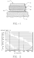
- Figure 1 schematically illustrates a four layer antireflection coating.
- Figure 2 is a graphical representation illustrating computed reflection values as a function wavelength of a four layer antireflection coating in accordance with the present invention.
- Figure 3 is a graphical representation illustrating computed reflection values as a function of wavelength for a four layer antireflection coating using titanium dioxide and silicon dioxide.
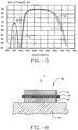
- FIG. 4 schematically illustrates an enhanced reflector coating in accordance with the present invention.
- Figure 5 is a graphical representation illustrating computed reflection values as a function of wavelength for a four layer enhanced reflector coating produced in accordance with the present invention.
- Figure 6 schematically illustrates a three layer low emissivity coating produced in accordance with the present invention.
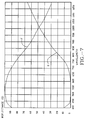
- Figure 7 is a graphical representation illustrating computed reflection and transmission values as a function of wavelength for a low emissivity coating produced in accordance with the present invention.
- the present invention is directed to processes for producing multilayer coatings incorporating at least one DC reactively sputtered niobium oxide (Nb 2 O 5 ) layer. These layers are durable and absorb very little, if any, visible light.
- Niobium oxide has a refractive index of about 2.35 at a wavelength of about 510 nm. It may be deposited about six times faster than titanium dioxide. As such, the use of niobium oxide in place of titanium oxide can provide a three-fold increase in the production rate. Moreover, the increased rate of production is achieved without a loss in optical performance. Indeed, the DC reactively sputtered niobium oxide has a lower dispersion than titanium oxide which results in improved performance for certain systems.
- the niobium oxide layers may be deposited, by DC reactive sputtering, in an ILS 1600 in-line sputtering apparatus available from Airco Coating Technologies of Fairfield, CA.
- the sputtering cathode can be a 6" round planar magnetron obtainable from VacTec Inc. in Boulder CO.
- the target may be made from 99.9% niobium obtainable from Cerac Inc. of Milkwaukee, WI.
- the niobium oxide may be sputtered at a voltage of -604 volts, and a sputtering pressure of 3.8 millitorr.
- the sputtering gas may be a mixture of argon and oxygen wherein the flow rate for the oxygen and argon is about 14.5 sccm (standard cubic centimeters per minute) and 45 sccm, respectively.
- Layers of various thickness are deposited by maintaining the above-described sputtering conditions and varying the rate at which substrates pass beneath the cathodes.
- the optical constants of a niobium oxide layer, i . e . the refractive index (n) and the extinction coefficient (k), are determined from reflection and transmission measurements of layers of known physical thickness. Sample results at different wavelengths are given in Table 1.
- titanium dioxide At a wavelength of 520 nm, nominally in the middle of the visible spectrum, titanium dioxide will have a refractive index of about 2.35, which is about the same as the refractive index of niobium oxide. At a wavelength of 400 nm, titanium dioxide will have a refractive index of about 2.54, and the refractive index of niobium oxide will be about 2.428. At a wavelength of 700 nm, titanium dioxide will have a refractive index of about 2.26 compared with 2.30 for niobium oxide. As can be seen, the niobium oxide layers are significantly less dispersive than the titanium dioxide layers, while having essentially the same refractive index in the middle of the visible spectrum.
- the deposition rate for the niobium oxide is up to about five times faster than that of titanium dioxide under the same sputtering conditions.
- the niobium oxide layers are as abrasion and scratch resistant as titanium oxide layers. Thus, niobium oxide layers may be substituted for titanium dioxide layers in optical coatings without compromising the optical or physical properties of the system.
- the coatings produced in accordance with the present invention may be in the form of a Rock-type antireflection coating.
- the coating or layer system 10 may be formed on a glass or plastic substrate 14.
- the refractive index of substrate 14 may be about 1.52 at a wavelength of about 520 nm.
- the coating 10 comprises a series of layers 12, 16, 18 and 20.
- the first or outermost layer 12 has a low refractive index, preferably lower than that of substrate 14.
- the optical thickness of layer 12 is about one-quarter wavelength at a wavelength of about 510 nm.
- the second layer 16 has a high refractive index and an optical thickness about twice that of layer 12.
- the third layer 18 has a relatively low refractive index, and fourth layer 20 has a high refractive index.
- the total optical thickness of layers 18 and 20 is generally less than about one-quarter wavelength at a wavelength of about 510 nm.
- the refractive indices of layers 12 and 16 must have a specific relationship to yield the lowest reflection across the visible spectrum.
- the preferred material for layer 12 is silicon dioxide. This material is preferred because it is durable and readily deposited by DC reactive sputtering. Silicon dioxide has a refractive index of about 1.46 at a wavelength of about 520 nm and the physical thickness of layer 12 may be about 85.2 nm. Layer 18 is also preferably silicon dioxide, and its physical thickness may be about 35.1 nm.
- Layers 16 and 20 are DC reactively sputtered niobium oxide.
- Layer 16 has a physical thickness of about 113.9 nm and layer 20 has a physical thickness of about 11.8 nm.
- the refractive index of layers 16 and 20 is about 2.35 at a wavelength of about 520 nm.
- the computed reflection performance for coating 10 on substrate 14 is shown in Figure 2.
- Figure 3 shows the computed reflection performance for a four layer system like that of Figure 1 wherein the outermost layer is silicon dioxide having a physical thickness of about 87.2 nm.
- the second and fourth layers are titanium dioxide with physical thicknesses of about 109.2 nm and 16.8 nm, respectively.
- the third layer is silicon dioxide having a physical thickness of about 30.8 nm.
- the refractive index of the substrate is about 1.52 at a wavelength of about 520 nm.
- FIG. 2 A comparison of Figure 2 and Figure 3 indicates that the substitution of niobium oxide for titanium dioxide in the four layer coating has no adverse effect on its optical performance.
- the coating obtainable by the present invention may be deposited about three times faster than a coating using titanium dioxide.
- the coating also has a slightly superior optical performance.
- the reflection values for coating 10 at the extremes of the visible spectrum, i . e . at about 425 nm and 675 nm, are lower by a factor of two. This performance differential is due to the lower index dispersion of the niobium oxide layers compared with the titanium dioxide layers.
- FIG. 4 another embodiment produced in accordance with the present invention is a multilayer enhanced reflector coating 22.
- the layer system 22 comprises a metal layer 24 adjacent to substrate 26.
- the coating 22 further includes low refractive index layers 28 and 32, and high refractive index layers 30 and 34.
- the optical thickness of each layer 28, 30, 32, and 34 is about one-quarter wavelength at a wavelength of about 510 nm.
- the substrate 26 may be any material on which a polished, or specular reflecting surface, may be created.
- the coating 22 is configured to be viewed in the direction shown by Arrow A.
- the layer 24 of coating 22 may be aluminum having a physical thickness of about 200 nm.
- the layers 28 and 32 may be silicon dioxide with a physical thickness of about 75.3 nm and 90.6 nm, respectively.
- the layers 30 and 34 are DC reactively sputtered niobium oxide having a physical thickness of about 50.5 nm and 50.7 nm, respectively.
- the computed reflection values for coating 22 having such dimensions is shown by Curve B of Figure 5.
- Curve C of figure 5 shows the performance of a coating using titanium dioxide instead of niobium oxide.
- a coating comprises an aluminum layer adjacent the substrate and having a physical thickness of about 200 nm.
- the silicon dioxide layers have a physical thickness of about 79.8 nm and 92.6 nm, respectively.
- the innermost and outermost titanium dioxide layers have a physical thickness of about 50.3 nm and 50.6 nm, respectively.
- Curves B and C indicate that the reflection performance of the two coatings in the visible spectrum is about the same.
- the niobium oxide coating 22 has a significantly higher reflectivity at the extremes of the visible spectrum, i . e . at about 425nm and 675 nm. This is due to the fact that niobium oxide has a lower dispersion than titanium dioxide.
- the niobium oxide-based coating may also be deposited at a rate about fifty percent faster than that of a titanium oxide-based coating.
- the low E coating or layer system 36 comprises a metal layer 38 bounded on either side by transparent dielectric layers 40 and 42.
- Layer 30 may be silver having a physical thickness of about 13.9 nm.
- Layers 40 and 42 are DC reactively sputtered niobium oxide with a physical thickness of about 34.4 and 36.6 nm, respectively.
- the substrate 44 may be glass or plastic. The layer system is viewed in the direction of Arrow D.
- the low E coating 36 may also use gold or copper for metal layer 38.
- the thickness of layer 38 may be between about 5 and 25 nm, depending on the metal layer, materials 40 and 42, and the desired optical performance.
- Multilayer optical coatings can be deposited by DC reactive sputtering in an in-line sputtering machine. These may include various antireflection coatings, multilayer dielectric mirrors and bandpass filters.
- Multilayer dielectric reflectors include a plurality of alternating high and low refractive index materials having an optical thickness of about one-quarter wavelength at the wavelength at which maximum reflection is desired.
- Bandpass filters can include multilayer dielectric reflectors and one or more layers about one-half wavelength in optical thickness. It viii be apparent from the above that should coatings require one or more layers having a refractive index of about 2.35, niobium oxide may be used in preference to titanium dioxide to increase the speed of the deposition process.
- niobium oxide Nb 2 O 5
- these layers may include various sub-oxides of Niobium.
- impurities or dopants may be involved in niobium oxide layer to increase the conductivity of the niobium oxide layer and potentially increase the sputtering rate.
Landscapes
- Chemical & Material Sciences (AREA)
- Physics & Mathematics (AREA)
- Inorganic Chemistry (AREA)
- Engineering & Computer Science (AREA)
- General Chemical & Material Sciences (AREA)
- Geochemistry & Mineralogy (AREA)
- Materials Engineering (AREA)
- Organic Chemistry (AREA)
- Life Sciences & Earth Sciences (AREA)
- Chemical Kinetics & Catalysis (AREA)
- General Physics & Mathematics (AREA)
- Optics & Photonics (AREA)
- Surface Treatment Of Glass (AREA)
- Surface Treatment Of Optical Elements (AREA)
- Chemically Coating (AREA)
- Physical Vapour Deposition (AREA)
- Laminated Bodies (AREA)
- Optical Filters (AREA)
Abstract
Description
- The present invention relates generally to processes for producing multilayer optical coatings for transparent substrates, and more particularly to such processes wherein the layers are deposited by DC reactive sputtering.
- DC reactive sputtering is the process most often used for large area commercial coating applications. Metal oxide layers, for example, are deposited by sputtering the appropriate metal in an atmosphere including oxygen. In the reactive sputtering process, the articles to be coated are passed through a series of in-line vacuum chambers each including sputtering sources. The chambers are isolated from one another by vacuum locks. Such a system may be referred to as an in-line system or simply a glass coater.
- Multilayer antireflection coatings are made by depositing two or more layers of transparent dielectric materials on a substrate. At least one of the layers has a refractive index higher than that of the substrate on which the coating. The coatings may be designed to reduce reflection at all wavelengths in the visible spectrum. The coatings may yield reflection values less than 0.25 percent over the visible spectrum.
- The time it takes to deposit a coating is determined mainly by the number of layers and the sputtering rate of the materials. The use of a glass coater to deposit multilayer antireflection coatings can significantly reduce their cost and thus extend their range of application. Such coatings may be used on picture frame glass and a display case, and as thermal control coatings for architectural and automobile glazings.
- Most multilayer antireflection coatings are derived from a basic three layer system. The first or outermost layer of the system has a refractive index lower than that of the substrate and an optical thickness of about one-quarter wavelength at a wavelength of about 520 nanometers (nm). The second or middle layer has a refractive index higher than that of the substrate, and an optical thickness of about one-half wavelength at a wavelength of about 520 nm. The third layer, i.e. the layer deposited on the substrate, has a refractive index greater than that of the substrate but less than the refractive index of the second layer. The optical thickness of the third layer is about one-quarter wavelength at a wavelength of about 520 nm. This basic design was first described in the paper entitled "Three Layered Reflection Reducing Coatings", J. Opt. Soc. Am., Vol. 37, Lockhart and King, pp. 689-694 (1947).
- A disadvantage of the basic three layer system is that the refractive indices of the layers must have specific values in order to produce the lowest reflectivity. The selection and control of the refractive index of the third layer is particularly important. Departure from specific values of refractive index can not be compensated for by varying the thicknesses of the layers.
- A simple improvement on the Lockhart and King system is described in U.S. Patent No. 3,432,225, issued to Rock. The Rock system includes four layers. The first or outermost layer has a refractive index lower than that of the substrate and an optical thickness of about one-quarter wavelength at a wavelength of about 520 nm. The second or middle layer has a refractive index higher than that of the substrate and an optical thickness of about one-half to sixth-tenths of a wavelength at a wavelength of about 520 nm. The third layer has a thickness of about one-tenth of a wavelength at a wavelength of about 520 nm. The refractive index of the third layer is less than that of the second layer. The fourth layer has an optical thickness of about one-tenth of a wavelength at a wavelength of about 520 nm, and a refractive index greater than that of the third layer and the substrate. The third layer may be the same material as the first layer and the fourth layer may be the same material as the second layer.
- The Rock system may be used with different combinations of materials. Differences in refractive indices may be compensated for by different layer thicknesses. Magnesium fluoride (MgF2)can be used to form the outer and third layers. If a higher refractive index material were used for the outer layer, then the refractive index of the second layer would also need to be higher to produce the lowest reflectivity.
- Magnesium fluoride may be deposited by sputtering but requires a reactive atmosphere including fluorine or hydrogen fluoride. In a layer system, designed for deposition by DC reactive sputtering in a glass coater, the outer layer is usually silicon dioxide (SiO2). Silicon dioxide has a refractive index of about 1.46 at a wavelength of about 520 nm. If the reactive index of the first layer is about 1.46, a second layer having a refractive index of about 2.35 would provide the lowest reflection over the visible spectrum. Titanium dioxide (TiO2) has a refractive index of about 2.35 at a wavelength of about 520 nm. As such, it is commonly used as the high refractive index material in a system deposited by DC reactive sputtering.
- The Rock system may require approximately equal thicknesses of titanium dioxide and silicon dioxide. Silicon dioxide may be sputtered four times faster than titanium dioxide. In order to operate at optimum speed, a glass coater may require four times as many sputtering cathodes for titanium dioxide as for silicon dioxide. However, the coater may not have enough chambers to accommodate all of these titanium dioxide cathodes. Thus, the deposition rate for the silicon dioxide will have to be reduced to "keep pace" with the deposition rate of the titanium dioxide. This reduces output and increases production costs.
- Materials such as tin oxide (SnO2) zinc oxide (ZnO) may be deposited by DC reactive sputtering at a rate at least six times faster than that of titanium oxide. These materials, however, have a refractive index of about 1.9 at a wavelength of 520 nm. The photopic reflection of a four layer antireflection coating using zinc oxide or tin oxide as the second layer would only be about 0.4 percent.
- The low DC reactive sputter rate for titanium dioxide also presents difficulties in the deposition of highly-reflecting coatings. Highly-reflecting coatings include enhanced metal reflectors which have a metal layer overcoated with low and high refractive index materials. Enhanced reflectors may have four such overcoating layers, including two high and two low refractive index layers arranged alternately. The overcoating layers each have an optical thickness of about one-quarter wavelength at a wavelength of about 520 nm. A low refractive index layer is in contact with the metal layer. The refractive index of the high refractive index material should be as high as possible and the refractive index of the low refractive index material should be as low as possible. This provides optimum reflection enhancement. The high and low index materials should also not absorb visible light.
- In the architectural glass coating industry, zinc oxide is used as a layer material for the formation of low emissivity (E) coatings. These coatings are designed to reflect long wavelength infrared radiation while transmitting visible light. They also have a low reflection for visible light from at least one surface. A low E coating may comprise three layers, for example, a silver layer bounded by two dielectric layers. The silver layer must be thick enough to provide high infrared reflection. The dielectric layers reduce reflection from the silver layer in the visible spectrum and thus enhance light transmission through the coated glass. The silver layer is preferably between about 10 and 15 nm thick. The refractive index of the dielectric layers should be relatively high. A material with a refractive index of about 2.35 at a wavelength of about 520 nm, such as titanium dioxide, would be preferred over zinc oxide for the reflection-reducing layers.
- Zinc oxide has a refractive index of about 1.9 at a wavelength of about 520 nm. The higher index permits the use of a thicker silver layer while maintaining low visible light transmission and high reflection. For example, using zinc oxide dielectric layers, a silver layer about 8 nm thick produces the lowest reflectivity. For titanium oxide dielectric layers, a silver layer about 130 nm thick produces the lowest reflectivity. The thicker silver layer may also provide higher reflection at longer wavelengths, i.e. a lower emissivity. The thicker silver layer may also provide a higher reflection and lower transmission in the near infrared spectrum, reducing the solar heat load. The industry preference for zinc oxide is substantially based on its high sputtering rate. The lower production costs afforded by the high sputtering rate may be sufficient to justify the less than optimum optical performance. The durability of a layer system incorporating zinc oxide is also poor due to zinc oxide's softness.
- It is widely believed that materials which can be deposited at high rates by DC reactive sputtering have relatively low refractive indices. Deposition rate comparisons may be slightly inconsistent from source to source. The type of machine and cathode used may also influence the results. The following approximate rate comparisons serve to illustrate the generalization. The refractive index values cited are the approximate values at a wavelength of about 520 nm. Titanium dioxide has a refractive index of about 2.35, and tantalum oxide (Ta2O5) has a refractive index of about 2.25. Tantalum oxide may be deposited at about twice the rate of titanium dioxide. Zirconium oxide (ZrO2) has a refractive index of about 2.15 and may be deposited at about twice the rate of titanium dioxide. Tin oxide has a refractive index of about 1.95 and may be deposited about ten times the rate of titanium dioxide. And zinc oxide has a refractive index of about 1.90 and may be deposited about ten times the rate of titanium dioxide.
- The above-described relationship between the refractive index and the sputtering rate implies that high deposition rates are achievable only with materials having relatively low refractive indices. A more probable explanation, however, is that zinc oxide and tin oxide are semiconductors. As such, oxide build-up on a sputtering target of zinc or tin may not create an insulating layer which lowers the sputtering rate. High oxygen-flow rates are thus possible in the sputtering gas without loss of power. A such, higher oxide deposition rates are possible.
- WO-A-9110564 discloses a heatable vehicle windscreen which comprises a substrate onto which an oxide layer, which may be niobium oxide, is deposited by methods which may include sputtering. A thin metal layer is deposited on the oxide layer, and a further oxide layer is deposited on the metal layer.
- WO-A-914016 discloses a multilayer system with high infra-red reflection capacity. A layer of niobium oxide is provided on a carrier substrate, and a metal layer is provided on the niobium oxide layer. A further niobium oxide layer is provided on the metal layer.
- EP-A-0263541 discloses an anti-reflective four layer coating provided on a face plate. The coating comprises two niobium pentoxide layers and two silicon dioxide layers, alternately arranged and with one of the niobium pentoxide layers adjacent to the face plate.
- Accordingly, it is the object of the present invention to provide a process for production of a high refractive index material having a refractive index of approximately equal to that of titanium dioxide but which may be deposited by DC reactive sputtering at a rate at least four times faster than titanium dioxide and preferably at a rate comparable to zinc oxide.
- It is a further object of the present invention to provide a process for production of a high refractive index material having a high DC reactive sputtering rate which is durable and abrasion resistant.
- It is another object of the present invention to provide a simple process for obtaining an antireflection layer system which may be deposited at low cost in a large area, in-line sputtering machine.
- It is yet another object of the present invention to provide a simple process for obtaining an enhanced reflector coating which may be deposited at low cost in a large area in-line sputtering machine.
- The present invention is directed at processes for producing multilayer optical coatings comprising substantially at least one layer of niobium oxide deposited by DC in-line reactive sputtering. At least one other layer having a refractive index different from the niobium oxide layer adjoins the niobium oxide layer. The niobium oxide layer may comprise different oxides of niobium and may include certain impurities or dopants. The optical coating may be, for example, an antireflection coating or an enhanced metal reflector.
- According to the present invention, there is provided a process according to
claim 1. - Preferred features of the process are defined in
claims 2 to 15. - The niobium oxide layer may be deposited two to five times faster than titanium dioxide, under the same sputtering conditions. The refractive index of the niobium oxide layer is about 2.45 at a wavelength of about 400nm, 2.35 at wavelength of about 520nm, and 2.30 at a wavelength of about 700nm.
- A four layer antireflection coating including niobium oxide and silicon dioxide layers may have a photopic reflectivity less than about 0.15 percent.
- Coatings including niobium oxide layers may be less expensive to produce since they may be deposited at high production rates. The lower cost may extend the application of such coatings to new and useful areas such as antireflection coatings on architectural and automobile glazings.
- The accompanying drawings,which are incorporated in and constitute a part of the specification, schematically illustrate a preferred embodiment of the present invention, and together with the general description given above and the detailed description of the preferred embodiment given below serve to explain the principles of the invention.
- Figure 1 schematically illustrates a four layer antireflection coating.
- Figure 2 is a graphical representation illustrating computed reflection values as a function wavelength of a four layer antireflection coating in accordance with the present invention.
- Figure 3 is a graphical representation illustrating computed reflection values as a function of wavelength for a four layer antireflection coating using titanium dioxide and silicon dioxide.
- Figure 4 schematically illustrates an enhanced reflector coating in accordance with the present invention.
- Figure 5 is a graphical representation illustrating computed reflection values as a function of wavelength for a four layer enhanced reflector coating produced in accordance with the present invention.
- Figure 6 schematically illustrates a three layer low emissivity coating produced in accordance with the present invention.
- Figure 7 is a graphical representation illustrating computed reflection and transmission values as a function of wavelength for a low emissivity coating produced in accordance with the present invention.
- The present invention is directed to processes for producing multilayer coatings incorporating at least one DC reactively sputtered niobium oxide (Nb2O5) layer. These layers are durable and absorb very little, if any, visible light. Niobium oxide has a refractive index of about 2.35 at a wavelength of about 510 nm. It may be deposited about six times faster than titanium dioxide. As such, the use of niobium oxide in place of titanium oxide can provide a three-fold increase in the production rate. Moreover, the increased rate of production is achieved without a loss in optical performance. Indeed, the DC reactively sputtered niobium oxide has a lower dispersion than titanium oxide which results in improved performance for certain systems.
- The niobium oxide layers may be deposited, by DC reactive sputtering, in an ILS 1600 in-line sputtering apparatus available from Airco Coating Technologies of Fairfield, CA. The sputtering cathode can be a 6" round planar magnetron obtainable from VacTec Inc. in Boulder CO. The target may be made from 99.9% niobium obtainable from Cerac Inc. of Milkwaukee, WI. The niobium oxide may be sputtered at a voltage of -604 volts, and a sputtering pressure of 3.8 millitorr. The sputtering gas may be a mixture of argon and oxygen wherein the flow rate for the oxygen and argon is about 14.5 sccm (standard cubic centimeters per minute) and 45 sccm, respectively. Layers of various thickness are deposited by maintaining the above-described sputtering conditions and varying the rate at which substrates pass beneath the cathodes. The optical constants of a niobium oxide layer, i.e. the refractive index (n) and the extinction coefficient (k), are determined from reflection and transmission measurements of layers of known physical thickness. Sample results at different wavelengths are given in Table 1.
Table 1 Wavelength (nm) n k 380 2.490 0.002 400 2.451 0.001 420 2.428 0.000 440 2.408 0.000 470 2.382 0.000 510 2.352 0.000 550 2.332 0.000 600 2.317 0.000 650 2.307 0.000 700 2.300 0.000 750 2.297 0.000 850 2.293 0.000 - At a wavelength of 520 nm, nominally in the middle of the visible spectrum, titanium dioxide will have a refractive index of about 2.35, which is about the same as the refractive index of niobium oxide. At a wavelength of 400 nm, titanium dioxide will have a refractive index of about 2.54, and the refractive index of niobium oxide will be about 2.428. At a wavelength of 700 nm, titanium dioxide will have a refractive index of about 2.26 compared with 2.30 for niobium oxide. As can be seen, the niobium oxide layers are significantly less dispersive than the titanium dioxide layers, while having essentially the same refractive index in the middle of the visible spectrum.
- The deposition rate for the niobium oxide is up to about five times faster than that of titanium dioxide under the same sputtering conditions. The niobium oxide layers are as abrasion and scratch resistant as titanium oxide layers. Thus, niobium oxide layers may be substituted for titanium dioxide layers in optical coatings without compromising the optical or physical properties of the system.
- As shown in Figure 1, the coatings produced in accordance with the present invention may be in the form of a Rock-type antireflection coating. The coating or
layer system 10 may be formed on a glass orplastic substrate 14. The refractive index ofsubstrate 14 may be about 1.52 at a wavelength of about 520 nm. - The
coating 10 comprises a series oflayers outermost layer 12 has a low refractive index, preferably lower than that ofsubstrate 14. The optical thickness oflayer 12 is about one-quarter wavelength at a wavelength of about 510 nm. Thesecond layer 16 has a high refractive index and an optical thickness about twice that oflayer 12. Thethird layer 18 has a relatively low refractive index, andfourth layer 20 has a high refractive index. The total optical thickness oflayers layers - In DC reactively sputtered coatings, the preferred material for
layer 12 is silicon dioxide. This material is preferred because it is durable and readily deposited by DC reactive sputtering. Silicon dioxide has a refractive index of about 1.46 at a wavelength of about 520 nm and the physical thickness oflayer 12 may be about 85.2 nm.Layer 18 is also preferably silicon dioxide, and its physical thickness may be about 35.1 nm. -
Layers Layer 16 has a physical thickness of about 113.9 nm andlayer 20 has a physical thickness of about 11.8 nm. The refractive index oflayers substrate 14 is shown in Figure 2. - Figure 3 shows the computed reflection performance for a four layer system like that of Figure 1 wherein the outermost layer is silicon dioxide having a physical thickness of about 87.2 nm. The second and fourth layers are titanium dioxide with physical thicknesses of about 109.2 nm and 16.8 nm, respectively. The third layer is silicon dioxide having a physical thickness of about 30.8 nm. The refractive index of the substrate is about 1.52 at a wavelength of about 520 nm.
- A comparison of Figure 2 and Figure 3 indicates that the substitution of niobium oxide for titanium dioxide in the four layer coating has no adverse effect on its optical performance. The coating obtainable by the present invention, however, may be deposited about three times faster than a coating using titanium dioxide. The coating also has a slightly superior optical performance. For example, the reflection values for coating 10 (see Figure 2) at the extremes of the visible spectrum, i.e. at about 425 nm and 675 nm, are lower by a factor of two. This performance differential is due to the lower index dispersion of the niobium oxide layers compared with the titanium dioxide layers.
- As shown in Figure 4, another embodiment produced in accordance with the present invention is a multilayer enhanced
reflector coating 22. Thelayer system 22 comprises ametal layer 24 adjacent tosubstrate 26. Thecoating 22 further includes low refractive index layers 28 and 32, and high refractive index layers 30 and 34. The optical thickness of eachlayer substrate 26 may be any material on which a polished, or specular reflecting surface, may be created. Thecoating 22 is configured to be viewed in the direction shown by Arrow A. - The
layer 24 ofcoating 22 may be aluminum having a physical thickness of about 200 nm. Thelayers layers - Curve C of figure 5 shows the performance of a coating using titanium dioxide instead of niobium oxide. Specifically, such a coating comprises an aluminum layer adjacent the substrate and having a physical thickness of about 200 nm. The silicon dioxide layers have a physical thickness of about 79.8 nm and 92.6 nm, respectively. And the innermost and outermost titanium dioxide layers have a physical thickness of about 50.3 nm and 50.6 nm, respectively.
- A comparison of Curves B and C indicates that the reflection performance of the two coatings in the visible spectrum is about the same. However, the
niobium oxide coating 22 has a significantly higher reflectivity at the extremes of the visible spectrum, i.e. at about 425nm and 675 nm. This is due to the fact that niobium oxide has a lower dispersion than titanium dioxide. The niobium oxide-based coating may also be deposited at a rate about fifty percent faster than that of a titanium oxide-based coating. - Yet another embodiment is a low emissivity (E) coating 36 shown in Figure 6. The low E coating or
layer system 36 comprises ametal layer 38 bounded on either side by transparentdielectric layers Layer 30 may be silver having a physical thickness of about 13.9 nm.Layers substrate 44 may be glass or plastic. The layer system is viewed in the direction of Arrow D. - The computed reflection (curve E) and transmission (curve F) values for coating 36 is shown is Figure 7. A low E coating including titanium dioxide layers would have essentially the same optical performance. The niobium oxide system, however, may be deposited about three times faster than the titanium dioxide system.
- The low E coating 36 may also use gold or copper for
metal layer 38. The thickness oflayer 38 may be between about 5 and 25 nm, depending on the metal layer,materials - Many types of multilayer optical coatings can be deposited by DC reactive sputtering in an in-line sputtering machine. These may include various antireflection coatings, multilayer dielectric mirrors and bandpass filters. Multilayer dielectric reflectors include a plurality of alternating high and low refractive index materials having an optical thickness of about one-quarter wavelength at the wavelength at which maximum reflection is desired. Bandpass filters can include multilayer dielectric reflectors and one or more layers about one-half wavelength in optical thickness. It viii be apparent from the above that should coatings require one or more layers having a refractive index of about 2.35, niobium oxide may be used in preference to titanium dioxide to increase the speed of the deposition process.
- The above embodiments have been described as including niobium oxide (Nb2O5). It will be apparent to those familiar will the art that these layers may include various sub-oxides of Niobium. It will also be apparent that certain impurities or dopants may be involved in niobium oxide layer to increase the conductivity of the niobium oxide layer and potentially increase the sputtering rate.
Claims (15)
- A process for making an optical coating on a surface (14,26,44) comprising sputtering niobium oxide to form at least one film (16,20; 30,34; 40,42) of the optical coating, characterised in that at least one film (16,20; 30,34; 40,42) of the niobium oxide is DC reactively magnetron sputtered by means of an in-line sputtering apparatus and has an index of refraction equal to or greater than 2.3 at a wavelength less than or of about 700 nanometres.
- A process according to Claim 1, wherein the step of reactively magnetron sputtering said niobium oxide comprises sputtering at least one film (16,20; 30,34; 40,42) of niobium oxide substantially non-absorbing for visible light.
- A process according to Claim 1 or 2, further comprising the step of forming at least one other layer (12,18; 28,32) having a refractive index lower than that of the sputtered niobium oxide.
- A process according to Claim 3 for forming an anti-reflection coating having at least four layers substantially transparent to visible light on the surface (14,24,26) wherein the step of forming said at least one other layer comprises depositing a layer farthest from the surface (14,24,26) having an optical thickness of about one-quarter wavelength at a wavelength of about 520nm, and wherein the step of DC reactively magnetron sputtering niobium oxide comprises reactively magnetron sputtering niobium oxide to form a layer (20,30) between said surface (14,24,26) and said farthest layer and said niobium oxide layer having an optical thickness between about one-half and six-tenths of a wavelength at a wavelength of about 520nm.
- A process according to Claim 2 for forming an anti-reflection coating having four layers substantially transparent to visible light on the surface (14,24,26), the layers designated the first, second, third and fourth layers in consecutive numerical order beginning with the layer farthest from the surface (14,24,26), comprising the steps of reactively magnetron sputtering niobium oxide on the surface (14,24,26) to form the fourth layer (20), depositing on the fourth layer a layer having a refractive index lower than that of the sputtered niobium oxide to form the third layer (18), reactively magnetron sputtering niobium oxide on the third layer to form the second layer (16), and depositing on the second layer another layer having a refractive index lower than that of the sputtered niobium oxide to form the first layer (12).
- A process according to Claim 4 or 5, wherein said surface is a metal substrate (24).
- A process according to Claim 4 or 5, wherein said surface is a glass substrate (14,26).
- A process according to any one of Claims 3 to 4, wherein said at least one other layer (12,18; 28,32) includes silicon dioxide.
- A process according to Claim 2 further comprising the steps of forming at least one transparent dielectric layer (28) adjoining said layer (30) including niobium oxide and having a refractive index different from niobium oxide, and forming a metal layer (24) as the surface adjoining said dielectric layer (28).
- A process according to Claim 9, wherein the coating is a reflective coating and said dielectric layer (28) has a refractive index lower than niobium oxide, and said dielectric layer (28) and said layer (30) including niobium oxide each have an optical thickness of about one-quarter wavelength at a wavelength of about 510nm.
- A process according to claim 10, wherein said metal layer (24) comprises an aluminium layer.
- A process according to Claim 2, wherein the surface is an aluminium layer and the coating is a reflective coating, and at least four layers are deposited onto the aluminium layer (24), said four layers including a first niobium oxide layer (34) located farthest from said aluminium layer (24), a second niobium oxide layer (30), and two dielectric layers (28,32) having a refractive index lower than niobium oxide, wherein one of said dielectric layers (32) is located between said first and second niobium oxide layers and the second said dielectric layer (28) is located between said second niobium oxide layer (30) and said aluminium layer (24), said four layers each having an optical thickness of about one-quarter wavelength at a wavelength of about 510nm.
- A process according to any one of claims 9 to 12, wherein at least one said dielectric layer (28,32) includes silicon dioxide.
- A process according to Claim 2 wherein the surface is a substrate and four layers substantially transparent to visible light are deposited onto the substrate (14), said layers being designated the first, second, third and fourth layers in consecutive numerical order beginning with the layer farthest from the substrate (14);
said second (16) and fourth (20) layers being layers of reactively magnetron sputtered niobium oxide;
said third layer (18) having a refractive index lower than niobium oxide;
said first layer (12) having a refractive index lower than said substrate (14) and an optical thickness of about one-quarter wavelength at a wavelength of about 520nm;
said second layer (16) having an optical thickness between about one-half and six-tenths of a wavelength at a wavelength of about 520nm; and
said third (18) and fourth (20) layers having a total optical thickness less than the optical thickness of said first layer (12). - A process according to Claim 14, wherein said third (18) and fourth (20) layers have substantially different optical thickness.
Applications Claiming Priority (3)
| Application Number | Priority Date | Filing Date | Title |
|---|---|---|---|
| US57534590A | 1990-08-30 | 1990-08-30 | |
| US575345 | 1990-08-30 | ||
| PCT/US1991/005303 WO1992004185A1 (en) | 1990-08-30 | 1991-07-31 | Dc reactively sputtered optical coatings including niobium oxide |
Publications (3)
| Publication Number | Publication Date |
|---|---|
| EP0498884A1 EP0498884A1 (en) | 1992-08-19 |
| EP0498884A4 EP0498884A4 (en) | 1993-06-23 |
| EP0498884B1 true EP0498884B1 (en) | 1997-11-12 |
Family
ID=24299945
Family Applications (1)
| Application Number | Title | Priority Date | Filing Date |
|---|---|---|---|
| EP91918239A Expired - Lifetime EP0498884B1 (en) | 1990-08-30 | 1991-07-31 | Process for producing optical coatings including niobium oxide by dc in-line reactive sputtering |
Country Status (7)
| Country | Link |
|---|---|
| US (1) | US5372874A (en) |
| EP (1) | EP0498884B1 (en) |
| JP (1) | JPH05502310A (en) |
| AT (1) | ATE160107T1 (en) |
| CA (1) | CA2067765A1 (en) |
| DE (1) | DE69128192T2 (en) |
| WO (1) | WO1992004185A1 (en) |
Families Citing this family (64)
| Publication number | Priority date | Publication date | Assignee | Title |
|---|---|---|---|---|
| US5828493A (en) * | 1992-07-24 | 1998-10-27 | Dielectric Coating Industries | Reflectors |
| US5450238A (en) * | 1993-12-10 | 1995-09-12 | Viratec Thin Films, Inc. | Four-layer antireflection coating for deposition in in-like DC sputtering apparatus |
| FR2722493B1 (en) | 1994-07-13 | 1996-09-06 | Saint Gobain Vitrage | MULTI-LAYERED HYDROPHOBIC GLAZING |
| US5579162A (en) * | 1994-10-31 | 1996-11-26 | Viratec Thin Films, Inc. | Antireflection coating for a temperature sensitive substrate |
| FR2730990B1 (en) * | 1995-02-23 | 1997-04-04 | Saint Gobain Vitrage | TRANSPARENT SUBSTRATE WITH ANTI-REFLECTIVE COATING |
| US5744227A (en) * | 1995-04-03 | 1998-04-28 | Southwall Technologies Inc. | Antireflective coatings comprising a lubricating layer having a specific surface energy |
| US5719705A (en) * | 1995-06-07 | 1998-02-17 | Sola International, Inc. | Anti-static anti-reflection coating |
| JP3808917B2 (en) | 1995-07-20 | 2006-08-16 | オリンパス株式会社 | Thin film manufacturing method and thin film |
| US6212004B1 (en) * | 1996-05-10 | 2001-04-03 | Applied Coatings, Inc. | Reflector with directional control of visible and infra-red radiation |
| US6231999B1 (en) * | 1996-06-21 | 2001-05-15 | Cardinal Ig Company | Heat temperable transparent coated glass article |
| KR100614707B1 (en) * | 1997-06-25 | 2006-08-21 | 비라텍 틴 필름스, 인크. | Filter for flat panel display and manufacturing method of filter |
| US5851674A (en) * | 1997-07-30 | 1998-12-22 | Minnesota Mining And Manufacturing Company | Antisoiling coatings for antireflective surfaces and methods of preparation |
| US6262830B1 (en) | 1997-09-16 | 2001-07-17 | Michael Scalora | Transparent metallo-dielectric photonic band gap structure |
| US5907427A (en) | 1997-10-24 | 1999-05-25 | Time Domain Corporation | Photonic band gap device and method using a periodicity defect region to increase photonic signal delay |
| US6074730A (en) * | 1997-12-31 | 2000-06-13 | The Boc Group, Inc. | Broad-band antireflection coating having four sputtered layers |
| US6277485B1 (en) | 1998-01-27 | 2001-08-21 | 3M Innovative Properties Company | Antisoiling coatings for antireflective surfaces and methods of preparation |
| EP0947601A1 (en) * | 1998-03-26 | 1999-10-06 | ESSILOR INTERNATIONAL Compagnie Générale d'Optique | Organic substrate having optical layers deposited by magnetron sputtering and method for preparing it |
| US6744552B2 (en) * | 1998-04-02 | 2004-06-01 | Michael Scalora | Photonic signal frequency up and down-conversion using a photonic band gap structure |
| US6304366B1 (en) | 1998-04-02 | 2001-10-16 | Michael Scalora | Photonic signal frequency conversion using a photonic band gap structure |
| US6231992B1 (en) * | 1998-09-04 | 2001-05-15 | Yazaki Corporation | Partial reflector |
| EP1137608A1 (en) * | 1998-11-09 | 2001-10-04 | PPG Industries Ohio, Inc. | Solar control coatings and coated articles |
| US6410173B1 (en) | 1998-11-30 | 2002-06-25 | Denglas Technologies, Llc | Antireflection coatings and other multilayer optical coatings for heat-treatable inorganic substrates and methods for making same |
| US6353501B1 (en) | 1999-01-21 | 2002-03-05 | Viratec Thin Films, Inc. | Display panel filter connection to a display panel |
| US6396617B1 (en) | 1999-05-17 | 2002-05-28 | Michael Scalora | Photonic band gap device and method using a periodicity defect region doped with a gain medium to increase photonic signal delay |
| US6538794B1 (en) | 1999-09-30 | 2003-03-25 | D'aguanno Giuseppe | Efficient non-linear phase shifting using a photonic band gap structure |
| ATE286602T1 (en) * | 1999-11-10 | 2005-01-15 | Denglas Technologies Llc | NIOOXIDE-BASED LAYERS FOR OPTICAL THIN FILM COATINGS AND METHOD FOR THE PRODUCTION THEREOF |
| DE60033017T2 (en) * | 1999-11-30 | 2007-05-10 | Matsushita Electric Industrial Co., Ltd., Kadoma | SEMICONDUCTOR LASER, METHOD FOR THE PRODUCTION THEREOF AND OPTICAL PLATE DEVICE |
| US6414780B1 (en) | 1999-12-23 | 2002-07-02 | D'aguanno Giuseppe | Photonic signal reflectivity and transmissivity control using a photonic band gap structure |
| US6339493B1 (en) | 1999-12-23 | 2002-01-15 | Michael Scalora | Apparatus and method for controlling optics propagation based on a transparent metal stack |
| US6656260B2 (en) * | 1999-12-28 | 2003-12-02 | Kyocera Corporation | ZnS-series sintered material and method for producing the same, target using the ZnS-series sintered material, thin film, and optical recording medium using the thin film |
| US6587263B1 (en) | 2000-03-31 | 2003-07-01 | Lockheed Martin Corporation | Optical solar reflectors |
| CA2355021C (en) * | 2000-08-29 | 2004-11-02 | Hoya Corporation | Optical element having antireflection film |
| JP3510845B2 (en) * | 2000-08-29 | 2004-03-29 | Hoya株式会社 | Optical member having antireflection film |
| JP3779174B2 (en) * | 2000-11-13 | 2006-05-24 | Hoya株式会社 | Vapor deposition composition, method of forming antireflection film using the same, and optical member |
| GB2371562A (en) * | 2001-01-26 | 2002-07-31 | Gen Electric Co Plc | Coated reflector for a lamp |
| JP2003015175A (en) | 2001-04-27 | 2003-01-15 | Mitsubishi Electric Corp | Solid-state light source device |
| US6670763B2 (en) * | 2001-05-15 | 2003-12-30 | General Electric Company | Display lamp with reflector having IR-reflective coating |
| AU2002323522A1 (en) * | 2001-08-29 | 2003-03-18 | 3M Innovative Properties Company | Optical devices using shaped optical fibers and methods for making optical devices with shaped optical fibers |
| US6589657B2 (en) | 2001-08-31 | 2003-07-08 | Von Ardenne Anlagentechnik Gmbh | Anti-reflection coatings and associated methods |
| EP1748035B1 (en) * | 2002-03-01 | 2010-10-20 | Cardinal CG Company | Thin film coating having transparent base layer |
| US6919133B2 (en) | 2002-03-01 | 2005-07-19 | Cardinal Cg Company | Thin film coating having transparent base layer |
| US6783253B2 (en) | 2002-03-21 | 2004-08-31 | Guardian Industries Corp. | First surface mirror with DLC coating |
| WO2004005975A2 (en) * | 2002-07-10 | 2004-01-15 | Denglas Technologies, L.L.C. | Method of making stress-resistant anti-reflection multilayer coatings containing cerium oxide |
| US20050008784A1 (en) * | 2003-06-27 | 2005-01-13 | 3M Innovative Properties Company | Removal and replacement of antisoiling coatings |
| US20050136180A1 (en) * | 2003-12-19 | 2005-06-23 | 3M Innovative Properties Company | Method of coating a substrate with a fluoropolymer |
| TW200718790A (en) * | 2005-11-04 | 2007-05-16 | Applied Vacuum Coating Technologies Co Ltd | Low temperature sputtering anti-reflection layer structure on sheet and manufacturing method thereof |
| US20070236798A1 (en) * | 2006-04-05 | 2007-10-11 | Shelestak Larry J | Antireflective coating and substrates coated therewith |
| JP4793259B2 (en) * | 2006-12-27 | 2011-10-12 | コニカミノルタオプト株式会社 | Reflector |
| DE102007061419A1 (en) * | 2007-12-20 | 2009-06-25 | Fraunhofer-Gesellschaft zur Förderung der angewandten Forschung e.V. | Transparent plastic film for shielding electromagnetic waves and method for producing such a plastic film |
| JP2010231172A (en) * | 2009-03-04 | 2010-10-14 | Seiko Epson Corp | Optical article and manufacturing method thereof |
| JP5588135B2 (en) * | 2009-08-10 | 2014-09-10 | ホーヤ レンズ マニュファクチャリング フィリピン インク | Method for manufacturing optical article |
| US20110291113A1 (en) * | 2010-05-27 | 2011-12-01 | Philips Lumileds Lighting Company, Llc | Filter for a light emitting device |
| JP2012032690A (en) | 2010-08-02 | 2012-02-16 | Seiko Epson Corp | Optical article and manufacturing method thereof |
| EP2613358A2 (en) | 2012-01-04 | 2013-07-10 | OC Oerlikon Balzers AG | Double layer antireflection coating for silicon based solar cell modules |
| EP2803246B1 (en) * | 2012-01-10 | 2017-05-03 | Saint-Gobain Glass France | Transparent pane with electrically heatable coating |
| EP2803245B1 (en) * | 2012-01-10 | 2017-03-08 | Saint-Gobain Glass France | Transparent pane with electrically heatable coating |
| JP5953592B2 (en) * | 2012-06-29 | 2016-07-20 | 北川工業株式会社 | Transparent heat ray reflective laminate |
| TWI756606B (en) | 2012-07-16 | 2022-03-01 | 美商唯亞威方案公司 | Optical filter and sensor system |
| US9977157B2 (en) * | 2013-02-13 | 2018-05-22 | Guardian Europe S.à r.l. | Dielectric mirror |
| US9594195B2 (en) | 2013-02-13 | 2017-03-14 | Centre Luxembourgeois de Recherches Pour le Verre et la Ceramique (CRVC) SaRL | Dielectric mirror |
| TWI577543B (en) | 2013-12-30 | 2017-04-11 | 聖高拜塑膠製品公司 | Optical film exhibiting improved light to solar gain heat ratio |
| EP3136141A1 (en) | 2015-08-26 | 2017-03-01 | Saint-Gobain Performance Plastics Corporation | Infrared reflecting film |
| CN110824599B (en) | 2018-08-14 | 2021-09-03 | 白金科技股份有限公司 | Infrared band-pass filter |
| CN118028750B (en) * | 2024-01-30 | 2025-07-18 | 中国科学院赣江创新研究院 | Nano composite coating and preparation method and application thereof |
Citations (2)
| Publication number | Priority date | Publication date | Assignee | Title |
|---|---|---|---|---|
| US3432225A (en) * | 1964-05-04 | 1969-03-11 | Optical Coating Laboratory Inc | Antireflection coating and assembly having synthesized layer of index of refraction |
| EP0464701A2 (en) * | 1990-06-29 | 1992-01-08 | RENKER GmbH & Co. KG | Multilayered system with high reflective capability in the infrared spectrum and high transmissivity in the visible light range |
Family Cites Families (9)
| Publication number | Priority date | Publication date | Assignee | Title |
|---|---|---|---|---|
| BE787599A (en) * | 1971-08-16 | 1973-02-16 | Battelle Memorial Institute | ANTISOLAR FILTERING AND THERMAL INSULATION GLASS |
| AU561315B2 (en) * | 1984-10-29 | 1987-05-07 | Ppg Industries Ohio, Inc. | Sputtering films of metal alloy oxide |
| GB2179007B (en) * | 1985-08-12 | 1990-09-12 | Mitsubishi Electric Corp | Thermal head for printer |
| GB8621468D0 (en) * | 1986-09-05 | 1986-10-15 | Philips Nv | Display device |
| US4773717A (en) * | 1986-11-03 | 1988-09-27 | Ovonic Synthetic Materials Co. | Transparency having a second surface multilayer decorative coating |
| ES2077562T3 (en) * | 1987-07-22 | 1995-12-01 | Philips Electronics Nv | OPTICAL INTERFERENCE FILTER. |
| WO1991010564A1 (en) * | 1990-01-15 | 1991-07-25 | Renker Gmbh & Co Kg | Heatable windscreen |
| DE4006804A1 (en) * | 1990-03-03 | 1991-09-05 | Renker Gmbh & Co Kg Zweigniede | MULTI-LAYER SYSTEM WITH A HIGH REFLECTION CAPACITY IN THE INFRARED SPECTRAL AREA AND WITH A HIGH TRANSMISSION CAPACITY IN THE VISIBLE AREA |
| US5140457A (en) * | 1990-11-13 | 1992-08-18 | Bausch & Lomb Incorporated | Reflector for display lighting |
-
1991
- 1991-07-31 AT AT91918239T patent/ATE160107T1/en not_active IP Right Cessation
- 1991-07-31 EP EP91918239A patent/EP0498884B1/en not_active Expired - Lifetime
- 1991-07-31 JP JP3516938A patent/JPH05502310A/en active Pending
- 1991-07-31 WO PCT/US1991/005303 patent/WO1992004185A1/en not_active Ceased
- 1991-07-31 DE DE69128192T patent/DE69128192T2/en not_active Expired - Fee Related
- 1991-07-31 CA CA002067765A patent/CA2067765A1/en not_active Abandoned
-
1993
- 1993-10-19 US US08/139,327 patent/US5372874A/en not_active Expired - Lifetime
Patent Citations (2)
| Publication number | Priority date | Publication date | Assignee | Title |
|---|---|---|---|---|
| US3432225A (en) * | 1964-05-04 | 1969-03-11 | Optical Coating Laboratory Inc | Antireflection coating and assembly having synthesized layer of index of refraction |
| EP0464701A2 (en) * | 1990-06-29 | 1992-01-08 | RENKER GmbH & Co. KG | Multilayered system with high reflective capability in the infrared spectrum and high transmissivity in the visible light range |
Non-Patent Citations (1)
| Title |
|---|
| SPIE vol. 678, pages 134-140 (1986): W.T. PAWLEWICS et al.: "Optical Thin Films II: New Developments - 1986: Multilayer coating fabrication by dc magnetron reactive sputtering" * |
Also Published As
| Publication number | Publication date |
|---|---|
| EP0498884A4 (en) | 1993-06-23 |
| DE69128192D1 (en) | 1997-12-18 |
| DE69128192T2 (en) | 1998-05-28 |
| EP0498884A1 (en) | 1992-08-19 |
| JPH05502310A (en) | 1993-04-22 |
| CA2067765A1 (en) | 1992-03-01 |
| ATE160107T1 (en) | 1997-11-15 |
| US5372874A (en) | 1994-12-13 |
| WO1992004185A1 (en) | 1992-03-19 |
Similar Documents
| Publication | Publication Date | Title |
|---|---|---|
| US5372874A (en) | DC reactively sputtered optical coatings including niobium oxide | |
| EP0795106B1 (en) | Antireflection coating for a temperature sensitive substrate | |
| EP1423737B1 (en) | Anti-reflection coatings and associated methods | |
| EP0505547B1 (en) | D.c. reactively sputtered antireflection coatings | |
| US5270858A (en) | D.C. reactively sputtered antireflection coatings | |
| US4971843A (en) | Non-iridescent infrared-reflecting coated glass | |
| KR100763543B1 (en) | Transparent substrate with low emissivity anti-glare or infrared absorption coating | |
| US5362552A (en) | Visible-spectrum anti-reflection coating including electrically-conductive metal oxide layers | |
| EP0933654B1 (en) | Anti-reflection coatings | |
| US5450238A (en) | Four-layer antireflection coating for deposition in in-like DC sputtering apparatus | |
| EP0548972B1 (en) | A transparent film-coated substrate | |
| EP0509050B1 (en) | Magnesium film reflectors | |
| US5298312A (en) | Non-iridescent transparent product | |
| JPH0570580B2 (en) | ||
| CA1264996A (en) | Non-iridescent infrared-reflecting coated glass | |
| JP2576637B2 (en) | Heat ray reflective glass | |
| JP2906524B2 (en) | Infrared reflective article | |
| HK1007899B (en) | Antireflection coating for a temperature sensitive substrate | |
| JPH05116992A (en) | Anti-glare transparent body |
Legal Events
| Date | Code | Title | Description |
|---|---|---|---|
| PUAI | Public reference made under article 153(3) epc to a published international application that has entered the european phase |
Free format text: ORIGINAL CODE: 0009012 |
|
| 17P | Request for examination filed |
Effective date: 19920421 |
|
| AK | Designated contracting states |
Kind code of ref document: A1 Designated state(s): AT BE CH DE DK ES FR GB GR IT LI LU NL SE |
|
| A4 | Supplementary search report drawn up and despatched |
Effective date: 19930504 |
|
| AK | Designated contracting states |
Kind code of ref document: A4 Designated state(s): AT BE CH DE DK ES FR GB GR IT LI LU NL SE |
|
| 17Q | First examination report despatched |
Effective date: 19940308 |
|
| GRAG | Despatch of communication of intention to grant |
Free format text: ORIGINAL CODE: EPIDOS AGRA |
|
| GRAH | Despatch of communication of intention to grant a patent |
Free format text: ORIGINAL CODE: EPIDOS IGRA |
|
| GRAH | Despatch of communication of intention to grant a patent |
Free format text: ORIGINAL CODE: EPIDOS IGRA |
|
| GRAA | (expected) grant |
Free format text: ORIGINAL CODE: 0009210 |
|
| AK | Designated contracting states |
Kind code of ref document: B1 Designated state(s): AT BE CH DE DK ES FR GB GR IT LI LU NL SE |
|
| PG25 | Lapsed in a contracting state [announced via postgrant information from national office to epo] |
Ref country code: GR Free format text: LAPSE BECAUSE OF FAILURE TO SUBMIT A TRANSLATION OF THE DESCRIPTION OR TO PAY THE FEE WITHIN THE PRESCRIBED TIME-LIMIT Effective date: 19971112 Ref country code: ES Free format text: THE PATENT HAS BEEN ANNULLED BY A DECISION OF A NATIONAL AUTHORITY Effective date: 19971112 Ref country code: DK Free format text: LAPSE BECAUSE OF NON-PAYMENT OF DUE FEES Effective date: 19971112 Ref country code: AT Free format text: LAPSE BECAUSE OF FAILURE TO SUBMIT A TRANSLATION OF THE DESCRIPTION OR TO PAY THE FEE WITHIN THE PRESCRIBED TIME-LIMIT Effective date: 19971112 |
|
| REF | Corresponds to: |
Ref document number: 160107 Country of ref document: AT Date of ref document: 19971115 Kind code of ref document: T |
|
| REG | Reference to a national code |
Ref country code: CH Ref legal event code: EP |
|
| REF | Corresponds to: |
Ref document number: 69128192 Country of ref document: DE Date of ref document: 19971218 |
|
| ITF | It: translation for a ep patent filed | ||
| PG25 | Lapsed in a contracting state [announced via postgrant information from national office to epo] |
Ref country code: SE Free format text: LAPSE BECAUSE OF FAILURE TO SUBMIT A TRANSLATION OF THE DESCRIPTION OR TO PAY THE FEE WITHIN THE PRESCRIBED TIME-LIMIT Effective date: 19980212 |
|
| ET | Fr: translation filed | ||
| REG | Reference to a national code |
Ref country code: CH Ref legal event code: NV Representative=s name: TROESCH SCHEIDEGGER WERNER AG |
|
| PLBQ | Unpublished change to opponent data |
Free format text: ORIGINAL CODE: EPIDOS OPPO |
|
| PLBI | Opposition filed |
Free format text: ORIGINAL CODE: 0009260 |
|
| PLAV | Examination of admissibility of opposition |
Free format text: ORIGINAL CODE: EPIDOS OPEX |
|
| PLBI | Opposition filed |
Free format text: ORIGINAL CODE: 0009260 |
|
| PLAV | Examination of admissibility of opposition |
Free format text: ORIGINAL CODE: EPIDOS OPEX |
|
| PLBJ | Opposition found inadmissible |
Free format text: ORIGINAL CODE: 0009275 |
|
| 26 | Opposition filed |
Opponent name: SAINT-GOBAIN VITRAGE Effective date: 19980804 |
|
| 26 | Opposition filed |
Opponent name: PILKINGTON DEUTSCHLAND GMBH Effective date: 19980813 Opponent name: SAINT-GOBAIN VITRAGE Effective date: 19980804 |
|
| PLBF | Reply of patent proprietor to notice(s) of opposition |
Free format text: ORIGINAL CODE: EPIDOS OBSO |
|
| 26U | Opposition found inadmissible | ||
| NLR1 | Nl: opposition has been filed with the epo |
Opponent name: PILKINGTON DEUTSCHLAND GMBH Opponent name: SAINT-GOBAIN VITRAGE |
|
| PLBF | Reply of patent proprietor to notice(s) of opposition |
Free format text: ORIGINAL CODE: EPIDOS OBSO |
|
| PLBF | Reply of patent proprietor to notice(s) of opposition |
Free format text: ORIGINAL CODE: EPIDOS OBSO |
|
| PLBL | Opposition procedure terminated |
Free format text: ORIGINAL CODE: EPIDOS OPPC |
|
| PGFP | Annual fee paid to national office [announced via postgrant information from national office to epo] |
Ref country code: FR Payment date: 19990630 Year of fee payment: 9 |
|
| PGFP | Annual fee paid to national office [announced via postgrant information from national office to epo] |
Ref country code: DE Payment date: 19990702 Year of fee payment: 9 |
|
| PGFP | Annual fee paid to national office [announced via postgrant information from national office to epo] |
Ref country code: CH Payment date: 19990705 Year of fee payment: 9 |
|
| PGFP | Annual fee paid to national office [announced via postgrant information from national office to epo] |
Ref country code: NL Payment date: 19990712 Year of fee payment: 9 |
|
| PGFP | Annual fee paid to national office [announced via postgrant information from national office to epo] |
Ref country code: LU Payment date: 19990714 Year of fee payment: 9 |
|
| PGFP | Annual fee paid to national office [announced via postgrant information from national office to epo] |
Ref country code: BE Payment date: 19990729 Year of fee payment: 9 |
|
| PLBM | Termination of opposition procedure: date of legal effect published |
Free format text: ORIGINAL CODE: 0009276 |
|
| STAA | Information on the status of an ep patent application or granted ep patent |
Free format text: STATUS: OPPOSITION PROCEDURE CLOSED |
|
| 27C | Opposition proceedings terminated |
Effective date: 19990612 |
|
| NLR2 | Nl: decision of opposition | ||
| PG25 | Lapsed in a contracting state [announced via postgrant information from national office to epo] |
Ref country code: LU Free format text: LAPSE BECAUSE OF NON-PAYMENT OF DUE FEES Effective date: 20000731 Ref country code: LI Free format text: LAPSE BECAUSE OF NON-PAYMENT OF DUE FEES Effective date: 20000731 Ref country code: CH Free format text: LAPSE BECAUSE OF NON-PAYMENT OF DUE FEES Effective date: 20000731 Ref country code: BE Free format text: LAPSE BECAUSE OF NON-PAYMENT OF DUE FEES Effective date: 20000731 |
|
| BERE | Be: lapsed |
Owner name: VIRATEC THIN FILMS INC. Effective date: 20000731 |
|
| PG25 | Lapsed in a contracting state [announced via postgrant information from national office to epo] |
Ref country code: NL Free format text: LAPSE BECAUSE OF NON-PAYMENT OF DUE FEES Effective date: 20010201 |
|
| REG | Reference to a national code |
Ref country code: CH Ref legal event code: PL |
|
| PG25 | Lapsed in a contracting state [announced via postgrant information from national office to epo] |
Ref country code: FR Free format text: LAPSE BECAUSE OF NON-PAYMENT OF DUE FEES Effective date: 20010330 |
|
| NLV4 | Nl: lapsed or anulled due to non-payment of the annual fee |
Effective date: 20010201 |
|
| REG | Reference to a national code |
Ref country code: FR Ref legal event code: ST |
|
| PG25 | Lapsed in a contracting state [announced via postgrant information from national office to epo] |
Ref country code: DE Free format text: LAPSE BECAUSE OF NON-PAYMENT OF DUE FEES Effective date: 20010501 |
|
| REG | Reference to a national code |
Ref country code: GB Ref legal event code: IF02 |
|
| PGFP | Annual fee paid to national office [announced via postgrant information from national office to epo] |
Ref country code: GB Payment date: 20030730 Year of fee payment: 13 |
|
| PG25 | Lapsed in a contracting state [announced via postgrant information from national office to epo] |
Ref country code: GB Free format text: LAPSE BECAUSE OF NON-PAYMENT OF DUE FEES Effective date: 20040731 |
|
| GBPC | Gb: european patent ceased through non-payment of renewal fee |
Effective date: 20040731 |
|
| PG25 | Lapsed in a contracting state [announced via postgrant information from national office to epo] |
Ref country code: IT Free format text: LAPSE BECAUSE OF NON-PAYMENT OF DUE FEES;WARNING: LAPSES OF ITALIAN PATENTS WITH EFFECTIVE DATE BEFORE 2007 MAY HAVE OCCURRED AT ANY TIME BEFORE 2007. THE CORRECT EFFECTIVE DATE MAY BE DIFFERENT FROM THE ONE RECORDED. Effective date: 20050731 |