EP0496637B1 - High purity conductive films and their use in semiconductors - Google Patents
High purity conductive films and their use in semiconductors Download PDFInfo
- Publication number
- EP0496637B1 EP0496637B1 EP92300634A EP92300634A EP0496637B1 EP 0496637 B1 EP0496637 B1 EP 0496637B1 EP 92300634 A EP92300634 A EP 92300634A EP 92300634 A EP92300634 A EP 92300634A EP 0496637 B1 EP0496637 B1 EP 0496637B1
- Authority
- EP
- European Patent Office
- Prior art keywords
- content
- contact barrier
- barrier layer
- leakage current
- diode
- Prior art date
- Legal status (The legal status is an assumption and is not a legal conclusion. Google has not performed a legal analysis and makes no representation as to the accuracy of the status listed.)
- Expired - Lifetime
Links
Images






Classifications
-
- H—ELECTRICITY
- H10—SEMICONDUCTOR DEVICES; ELECTRIC SOLID-STATE DEVICES NOT OTHERWISE PROVIDED FOR
- H10D—INORGANIC ELECTRIC SEMICONDUCTOR DEVICES
- H10D30/00—Field-effect transistors [FET]
- H10D30/60—Insulated-gate field-effect transistors [IGFET]
- H10D30/67—Thin-film transistors [TFT]
- H10D30/6729—Thin-film transistors [TFT] characterised by the electrodes
- H10D30/6737—Thin-film transistors [TFT] characterised by the electrodes characterised by the electrode materials
- H10D30/6738—Schottky barrier electrodes
-
- H—ELECTRICITY
- H10—SEMICONDUCTOR DEVICES; ELECTRIC SOLID-STATE DEVICES NOT OTHERWISE PROVIDED FOR
- H10D—INORGANIC ELECTRIC SEMICONDUCTOR DEVICES
- H10D30/00—Field-effect transistors [FET]
- H10D30/60—Insulated-gate field-effect transistors [IGFET]
- H10D30/67—Thin-film transistors [TFT]
- H10D30/674—Thin-film transistors [TFT] characterised by the active materials
- H10D30/675—Group III-V materials, Group II-VI materials, Group IV-VI materials, selenium or tellurium
-
- H—ELECTRICITY
- H10—SEMICONDUCTOR DEVICES; ELECTRIC SOLID-STATE DEVICES NOT OTHERWISE PROVIDED FOR
- H10D—INORGANIC ELECTRIC SEMICONDUCTOR DEVICES
- H10D64/00—Electrodes of devices having potential barriers
- H10D64/60—Electrodes characterised by their materials
- H10D64/64—Electrodes comprising a Schottky barrier to a semiconductor
Definitions
- This invention relates to semiconductor devices comprising high purity conductive films, including films which contact barrier layers or gate electrodes.
- a film such as a Ti film, etc.
- a contact barrier layer between a silicon substrate and aluminum wires, to prevent diffusion of silicon into aluminum wires.
- Materials for such contact barrier layers are required to have characteristics including low electrical resistance, high heat resistance, and chemical stability needed for LSI manufacturing process steps.
- applications of silicide films, high melting point metals, high melting point metal alloys or nitride films of Ti, Ta or Ti-W alloy have been considered, and some have been tried.
- the leakage current of semiconductor devices causes malfunctions and reduced reliability. Therefore, it is desirable to minimize leakage current, especially as the down-scaling of semiconductor devices continues in the future.
- Na and K are elements diffused easily in SiO 2 film.
- the elements move to the interface between a Si substrate and a SiO 2 gate insulating film. A portion of these elements are ionized resulting in positive charges, these charges generating the interface state. In this state, these charges tend to trap charge carriers in Si, such as the charge carriers flowing in the channel.
- heavy metal impurities such as Fe, Cr, and the like are included in higher concentration than Na and K and also move to the interface between a Si substrate and a gate insulating layer made of SiO 2 .
- the impurities cause the generation of an interface state and the fluctuation of threshold voltage.
- impurity concentration varies as a function of the manufacturing process
- materials for semiconductor devices typically contain about 1 x 10 19 cm -3 of each of the above-listed types of impurities. Some of these impurities are believed to act to increase leakage current in addition to such effects as generation of an interface state and deterioration of surface characteristics. Techniques known in the art have been successful in effecting reductions in leakage current. However, further reductions in leakage current will be required to improve device operation and to further control leakage current in view of the expected higher integration of semiconductor devices in the future.
- the present invention provides a semiconductor device including a contact barrier layer and/or a gate electrode either or both of which is constructed of high purity conductive film composed of conductive material whose impurity content of aluminium is 1 x 10 18 cm -3 .
- the conductive film may comprise at least one material selected from Ti, W, Mo, Zr, Hf, Ta, V, Nb, Ir, Fe, Ni, Cr, Co, Pd, and Pt, and most preferably comprises at least one kind of metal silicide including a metal selected from Ti, Wi, Mo, Zr, Hf, Ta, V, Nb, Ir, Fe, Ni, Cr, Co, Pd and Pt or the film comprises a nitride of T, T, or Ti-W alloy.
- semiconductor devices constructed in accordance with the present invention are characterized by including the conductive films described above.
- Leakage current in semiconductor devices is induced by the effect of impurities contained in materials for the contact barrier layer or gate electrode proximate the source and drain areas.
- the present invention is based, in part, on the discovery by the present inventors of the dependence of the magnitude of leakage current on the Al concentration in the contact barrier layer or gate electrode material.
- Al was not regarded as a serious impurity in the prior art.
- the present inventors have discovered that Al contained in the conductive films, will segregate on an interface between the contact barrier layer and source electrode or drain electrode during a subsequent processing step during device fabrication. Such Al reacts with oxygen left on the interface to form Al 2 O 3 . It also appears that the Al will form Al 2 O 3 instead of deoxidizing a SiO 2 film in the device. These phenomena result in an increase of the contact resistance at the junction between an aluminum contact and the source or drain area.
- the inventors studied the relationships between the Al contents in conductive films and contact resistance, which are detected in the contact barrier layers. As the result, it was discovered that an increase of the contact resistance value by the formation of Al 2 O 3 as described above is avoided by controlling the Al content of the conductive film to be below 1 x 10 18 cm -3 .
- the Al content in at least one of the contact barrier layer and the gate electrode of a semiconductor device is maintained at or below 1 x 10 18 cm -3 because if the Al content is above this value, leakage current will increase with the increase of Al content. Further, the semiconductor device becomes more susceptible to the effect of Al contained in the contact barrier layer with the decrease in the depth of the source and drain areas and leakage current will increase. However, if the Al content in at least one of the contact barrier layer and the gate electrode of a semiconductor device is maintained at or below 1 x 10 18 cm -3 , leakage current will be kept at nearly a constant level regardless of the depth of the source and drain areas.
- the conductive films made of TiN, Mo, W, TiSi 2 and CoSi 2 of the present invention are preferred for practical use because they have excellent thermal stability as well as chemical stability. Furthermore, such films have an effect to reduce contact resistance when used for the contact barrier layer.
- the conductive film of the present invention is effective for reducing leakage current in.a semiconductor device irrespective of whether the film and device are constructed of either crystalline or amorphous material.
- thermal stability in the amorphous state is less satisfactory, however such metals as Ta-Ir, Ni-Nb, Fe-W, etc., are relatively stable and can be successfully used in the amorphous state. Since such amorphous alloys have no grain boundary, Al does not diffuse at a high speed and, as a result, the leakage current is restrained further.
- the conductive film of the present invention can be produced, for example, in the following manner.
- the sputtering method which is generally used for forming the conductive film of semiconductor devices, is used.
- the Al content in the conductive film is suppressed by reducing the Al concentration in the sputtering target.
- the Al content in the resulting conductive film directly corresponds to the Al content in the sputtering target.
- the Al content in a Ti-W alloy or Mo silicide film is suppressed to below 30 ppm.
- the conductive film is produced by sputtering using these kinds of targets.
- the Al content in the conductive film can be suppressed to below 1 x 10 18 cm -3 by performing the active sputtering in a nitrogen gas atmosphere with the Al content in a Ti, Ta, W, or Ti-W alloy target suppressed to below 30 ppm.
- the conductive film of the present invention is also formed using the chemical vapor deposition (CVD) method.
- the Al content in the film can be suppressed to a low level by reducing the Al concentration in the gas used to perform the CVD.
- FIG. 17 illustrates a semiconductor diode 10 comprising an n-type silicon substrate 3, a p + area 2 formed in the surface of substrate 3, and an insulating layer 5 of SiO 2 formed on the substrate.
- An aperture 6 formed in the layer 5 exposes a portion of the p + area 2 on which is deposited a contact barrier layer 1.
- An Al contact layer 4 is deposited over the contact barrier layer 1.
- the diode 10 was produced to have structure similar to that of the contact section of a MOSFET device.
- the depth of p + area 2 is similar to the depth of the source or drain area of a MOSFET constructed in accordance with the same design rule. Specific device dimensions are provided below.
- a diode was produced by forming the contact barrier layer 1 made of Ti-W on the p + area 2 formed on the n type substrate 3 and by forming the Al layer 4 on the contact barrier layer 1 as shown in Figure 17.
- the depth of the source and drain areas of this diode was about 0.3 ⁇ m and the area of the aperture 6 was 1.5 x 1.5 ⁇ m 2 .
- the contact barrier layer was formed by the following steps:
- a high purity W powder (maximum particle size of 10 ⁇ m or below, mean particle size of 4 ⁇ m) was mixed for 48 hours with a high purity Ti powder (maximum particle size of 50 ⁇ m or below, mean particle size of 30 ⁇ m) in the ratio of 10 wt% Ti-W (i.e., 10 wt% Ti and 90 wt% W) using a ballmill filled with high purity Ar gas.
- a BN mold release was spread on a surface of a mold made of graphite and a Ta-plate was put on the surface of the mold. The mold was then filled with the mixed powder.
- the mold was inserted in a hot-press machine and the mixed powder in the mold was compacted and sintered for 3 hours under conditions of 5 x 10 -4 Torr, 1400°C, and a pressure of 250kg/cm 2 .
- the sintered body was shaped by machining to form a first target having approximate dimensions of 260mm diameter and 6mm thickness.
- the Al content of the target was approximately 0.8 ppm.
- a second target was produced in a manner similar to that described above, except without use of the Ta-plate on the mold.
- the Al content of the second target was 15 ppm.
- a high purity W powder (maximum particle size of 50 ⁇ m or below, mean particle size of 30 ⁇ m) was mixed for 48 hours with a high purity Ti powder (maximum particle size of 100 ⁇ m or below, mean particle size of 70 ⁇ m) in the ratio of 10 wt% Ti-W using a ballmill filled with high purity Ar gas.
- a third target was produced from this mixed powder in the manner described above without a Ta-plate in a mold. The Al content of the third target was 50 ppm.
- the contact barrier layer 1 in each of the three devices was formed as a Ti-W film using a different one of the first, second, and third targets described above.
- the Al content in each of Ti-W films was measured by frameless atomic absorption spectrophotometry.
- the values of the Al content of the films formed using the first, second, and third targets were 1 x 10 17 cm -3 , 1 x 10 18 cm -3 and 1 x 10 19 cm -3 , respectively.
- the thickness of layer 1 was about 80 nm.
- the relation between the Al content in the Ti-W contact barrier layer and pn junction leakage current was also evaluated.
- a reverse bias voltage was applied to each diode.
- the reverse bias voltage was initially 0V and was gradually increased.
- the leakage current of each diode was measured until breakdown occurred.
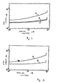
- the results of this investigation are plotted on the graph shown in Figure 1.
- the abscissa represents the applied reverse bias voltage and the ordinate represents the measured leakage current.
- Curve A shows the current-voltage characteristic of the diode with a Ti-W layer having an Al content of 1 x 10 19 cm -3 .
- Curve B corresponds to the diode with a Ti-W layer having an Al content of 1 x 10 18 cm -3 .
- Curve C corresponds to the diode with a Ti-W layer having an Al content of 1 x 10 17 cm -3 .
- the content of impurities other than aluminum was sufficiently low.
- the total content of heavy metals other than Al, Ti, and W was below 5 x 10 16 cm -3 and the total content of alkali metals was below 5 x 10 16 cm -3 .
- Two diodes 10 were constructed, each having a Mo contact barrier layer 1, with all other features of the diode having the same construction as in Embodiment 1.
- the relation between the Al content in the Mo contact barrier layer and the pn junction leakage current was investigated.
- the Mo contact barrier layers of the two diodes were respectively formed according to the CVD method using MoCl 5 gas having an Al concentration below 0.1 ppm with a very small quantity (about 500 ppm) of Al added and MoCl 5 gas having an Al concentration below 0.1 ppm.
- the Al contents of these two Mo films were 3 x 10 18 cm -3 and 3 x 10 17 cm -3 , respectively, when measured by frameless atomic absorption spectrophotometry.
- the thickness of the Mo layer in each device was about 100 nm.
- the measurement of leakage current was conducted according to the same method as in Embodiment 1.
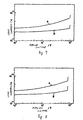
- the results of measurement of the pn junction leakage current value as a function of reverse bias voltage are shown in Figure 2.
- Curve A shows the current-voltage characteristic of a diode including the Mo contact barrier layer with an Al content of 3 x 10 18 cm -3
- Curve B shows the current-voltage characteristic of the diode having the Mo layer with an Al content of 3 x 10 17 cm -3 .
- the W contact barrier layers of the two diodes were respectively formed according to the CVD method using 0.1 ppm or less WF 6 gas with a very small quantity of Al (60 ppm) added and WF 6 gas with an Al concentration of 0.1 ppm.
- the Al contents of these two W layers were 0.5 x 10 19 cm - 3 and 4 x 10 17 cm -3 , respectively, when measured by frameless atomic absorption spectrophotometry. Further, the thickness of the W layer in each device was about 80 nm.
- the measurement of leakage current was conducted in the same manner as in Embodiment 1.
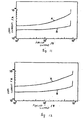
- the results of measurement of the pn junction leakage current value as a function of reverse bias voltage are shown in Figure 3.
- Curve A in Figure 3 shows the current-voltage characteristics of the diode having the W layer with an Al content of 0.5 x 10 19 cm -3 and Curve B shows that of the diode having the W layer with an Al content of 4 x 10 17 cm -3 .
- the content of heavy metal other than W was sufficiently low, i.e., below 1 x 10 17 cm -3 and the content of alkali metal was also low, i.e., below 3 x 10 16 cm - 3 .
- the leakage current is suppressed substantially by reducing the Al concentration in the contact barrier layer.
- Two diodes 10 were constructed, each having a Ta-Ir amorphous contact barrier layer 1, with all other features of the diode having the same construction as in Embodiment 1.
- the relation between the Al content in the Ta-Ir amorphous contact barrier layer and the pn junction leakage current was investigated.
- the Ta-Ir amorphous contact barrier layers of the two diodes were respectively formed by sputtering using 48.5 wt% Ta-Ir composite targets respectively having Al concentrations of 100 and 30 ppm.
- the Al contents of the respective layers were 8 x 10 18 cm -3 and 4 x 10 17 cm -3 .
- the contact barrier layer thickness was about 90 nm in each diode.
- the measurement of leakage current was conducted in the same manner as in Embodiment 1.
- Ni-Nb amorphous contact barrier layer 1 Two diodes were constructed, each having an Ni-Nb amorphous contact barrier layer 1, with all other features of the diode having the same construction as in Embodiment 1.
- the Ni-Nb amorphous contact barrier layers of the two diodes were respectively formed using 61 wt% Ni-Nb composite targets with Al concentrations of 180 and 10 ppm, respectively.
- the Al content in each Ni-Nb amorphous contact barrier layer was 1.5 x 10 19 cm -3 and 1 x 10 17 cm -3 .
- the layer thickness was about 90 nm.
- the measurement of leakage current was conducted in the same manner as in Embodiment 1.
- Two diodes 10 were constructed, each having a Fe-W amorphous contact barrier layer 1, with all other features of the diode having the same construction as in Embodiment 1.
- the relation between the Al content in the Fe-W amorphous contact barrier layer and the pn junction leakage current was investigated.
- the Fe-W amorphous contact barrier layers of the two diodes were respectively formed by sputtering using 23.3 wt% Fe-W composite targets having Al concentrations of about 150 and 15 ppm, respectively.
- the Al contents of the respective Fe-W amorphous contact barrier layers were 2.6 x 10 18 cm -3 and 1 x 10 17 cm -3 .
- the contact barrier layer thickness was about 90 nm in each diode.
- the measurement of leakage current was conducted in the same manner as in Embodiment 1.
- Two diodes 10 were constructed, each having a Ti silicide contact barrier layer 1, with all other features of the diode having the same construction as in Embodiment 1.
- the relation between the Al content in the Ti silicide contact barrier layer and the pn junction leakage current was investigated.
- the Ti silicide contact barrier layers of the two diodes were respectively formed according to the sputtering method using 56.0 wt% Ti-Si composite targets with Al concentrations of 150 and 15 ppm, respectively.
- a Ti-Si composite target (Al content 150 ppm) was produced by the following process.
- a quantity of Ti made by the Kroll process was melted by arc discharge to form a Ti ingot of 140mm diameter.
- the Ti ingot was hot-forged, grinded, polished, and shaped to form a Ti sputtering target.
- Si-blocks (purity 5N) were uniformly spaced apart on the Ti target surface in a checkerboard-like mosaic pattern to cover approximately 56% of the area of the Ti target.
- the Al content in each Si-block was 1 ppm or less.
- a Ti-Si composite target (Al content 10 ppm) was produced by the following process.
- An electrode made of sponge Ti was immersed into an electrolytic bath (KCl:16 wt%, NaCl: 84 wt%) and formed into Ti needles by the molten salt electrolysis method at conditions of 755°C, current 200A, and voltage 8V.
- the Ti needles were washed in a NaOH solution, to remove Al on the surface of the needles, and rinsed in water. After that, the Ti needles were melted by the electron beam melting method under conditions of 5 x 10 -5 mbar and 30kW and a Ti ingot of 135mm diameter was formed. The Ti ingot was cool-forged, grinded, polished, and shaped to form a Ti target.
- Si-blocks (purity 5N) were uniformly spaced apart on the Ti target surface in a checkerboard-like mosaic pattern to cover approximately 56% of the area of the Ti target.
- the Al content in each Si-block was 1 ppm or less.
- the Ti silicide layers were produced by the sputtering method and the Al contents in the layers were 5 x 10 18 cm -3 and 1 x 10 17 cm -3 , respectively, measured by frameless atomic absorption spectrophotometry.
- the layer thickness was about 90 nm in each diode.
- the measurement of leakage current was conducted in the same manner as in Embodiment 1.
- Two diodes 10 were constructed, each having a W-silicide contact barrier layer 1, with all other features of the diode having the same construction as in Embodiment 1.
- the relation between the Al content in the W-silicide contact barrier layer and the pn junction leakage current was investigated.
- the W-silicide contact barrier layers of the two diodes were respectively formed according to the sputtering method using 70.8 wt% W-Si composite targets having Al concentrations of about 150 and 0.3 ppm, respectively.
- the W-silicide targets were produced by the following process.
- High purity W powder (maximum particle size of 10 ⁇ m or less) was mixed for 48 hours with high purity Si powder (maximum particle size of 30 ⁇ m or below) in the ratio of 70.8 wt% W-Si using a ballmill filled with high purity Ar gas.
- a BN mold release was spread on a surface of a mold made of graphite and a Ta-plate was put on the surface of the mold. Then the mold was filled with the mixed powder.
- the mold was inserted in a hot-press machine and the mixed powder was changed to silicide under conditions of under 5 x 10 -4 Torr, 1250°C for 2 hours, and pressure of 50 kg/cm 2 . Then the silicide was deoxidized and decarbonized under conditions of 135°C for 5 hours and was compacted and sintered under conditions of 1400°C for 5 hours and pressure of 270 kg/cm 2 to form a sintered body.
- the sintered body was grinded, polished, and shaped by electrospark machining to form a first target of approximately 260mm diameter and 6mm thickness.
- the Al content in the first target was 0.3 ppm.
- Si powder Al content 450 ppm
- high purity W powder maximum particle size 10 ⁇ m or less
- a second target was produced in a similar manner to that described above for producing the first target.
- the Al content of the second target was 150 ppm.
- the Al contents of the respective W-silicide layers were 2.5 x 10 18 cm -3 and 1 x 10 16 cm -3 , respectively.
- the layer thickness was about 90 nm in each diode.
- the measurement of leakage current was conducted in the same manner as in Embodiment 1.
- Two diodes 10 were constructed, each having a Mo-silicide contact barrier layer 1, with all other features of the diode having the same construction as in Embodiment 1.
- the relation between the Al content in the Mo-silicide contact barrier layer and the pn junction leakage current was investigated.
- the Mo-silicide contact barrier layer was formed according to the sputtering method using 63.1 wt% No-Si composite targets having Al concentrations of about 150, 30 and 0.4 ppm, respectively.
- the Mo-silicide targets were produced by the following process.
- High purity Mo powder (maximum particle size was 10 ⁇ m or below) was mixed for 48 hours with high purity Si powder (maximum particle size of 30 ⁇ m or below) in the ratio of 63.1 wt% Mo-Si using a ballmill filled with high purity Ar gas.
- a BN mold release was spread on a surface of a mold made of graphite and a Ta-plate was put on the surface of the mold. Then the mold was filled with the mixed powder.
- the mold was inserted in a hot-press machine and the mixed powder was changed to silicide under conditions of under 5 x 10 -4 Torr, 1100°C for 2 hours, and pressure of 40 kg/cm 2 . Then the silicide was deoxidized and decarbonized under conditions of 1350°C for 5 hours and was compacted and sintered under conditions of 1400°C for 5 hours and pressure of 280 kg/cm 2 to form a sintered body.
- the sintered body was grinded, polished, and shaped by electrospark machining to form a first target of approximately 260mm diameter and 6mm thickness.
- the Al content in the first target was 0.4 ppm.
- Si powder Al content 120 ppm for a second target
- Si powder Al content 450 ppm for a third target
- high purity W powder maximum particle size 10 ⁇ m or below
- second and third targets were produced in a similar manner to that described above for the first target.
- the Al contents in the second and third targets were 150 ppm and 330 ppm, respectively.
- the Al contents of the respective W-silicide layers were 2 x 10 19 cm -3 and 1 x 10 18 cm -3 and 1 x 10 16 cm -3 , respectively.
- the layer thickness was about 90 nm in each diode.
- the measurement of leakage current was conducted in the same manner as in Embodiment 1.
- Two diodes 10 were constructed, each having a Ta-silicide contact barrier layer 1, with all other features of the diode having the same construction as in Embodiment 1.
- the relation between the Al content in the Ta-silicide contact barrier layer and the pn junction leakage current was investigated.
- the Ta-silicide contact barrier layers of the two diodes were respectively formed according to the sputtering method using 76.3 wt% Ta-Si composite targets having Al concentrations of about 150 ppm and 0.4 ppm, respectively.
- the Ta-silicide targets were produced by the following process.
- High purity Ta powder (maximum particle size of 10 ⁇ m or below) was mixed for 48 hours with high purity Si powder (maximum particle size of 30 ⁇ m or below) in the ratio of 76.31 wt% Ta-Si using a ballmill filled with high purity Ar gas.
- a BN mold release was spread on a surface of a mold made of graphite and a Ta-plate was put on the surface of the mold. Then the mold was filled with the mixed powder.
- the mold was inserted in a hot-press machine and the mixed powder was changed to silicide under conditions of under 5 x 10 -4 Torr, 1150°C for 3 hours, and pressure of 60 kg/cm 2 .
- the silicide was deoxidized and decarbonized under conditions of 1300°C for 5 hours and was compacted and sintered under conditions of 1360°C for 5 hours and pressure of 280 kg/cm 2 to form a sintered body.
- the sintered body was grinded, polished and shaped by electrospark machining to form a first target of approximately 260mm diameter and 6mm thickness.
- the Al content of the first target was 0.4 ppm.
- Si powder Al content 430 ppm
- high purity Ta powder maximum particle size 10 ⁇ m or below
- high purity Ar gas high purity Ar gas
- the Al contents of the respective Ta-silicide layers were 4 x 10 18 cm -3 and 2 x 10 17 cm -3 , respectively.
- the layer thickness was about 90 nm in each diode.
- the measurement of leakage current was conducted in the same manner as in Embodiment 1.
- Ni-silicide contact barrier layer 1 Two diodes were constructed, each having an Ni-silicide contact barrier layer 1, with all other features of the diode having the same construction as in Embodiment 1.
- the relation between the Al content in the Ni-silicide contact barrier layer and the pn junction leakage current was investigated.
- the Ni-silicide contact barrier layers of the two diodes were respectively formed according to the sputtering method using 51.1 wt% Ni-Si composite targets having Al concentrations of about 200 and 0.5 ppm, respectively.
- Ni-silicide targets were produced by the following process.
- High purity Ni powder (maximum particle size of 10 ⁇ m or less) was mixed for 48 hours with high purity Si powder (maximum particle size of 30 ⁇ m or less) in the ratio of 51.1 wt% Ni-Si using a ballmill filled with high purity Ar gas.
- a BN mold release was spread on a surface of a mold made of graphite and a Ta-plate was put on the surface of the mold. Then the mold was filled with the mixed powder.
- the mold was inserted in a hot-press machine and the mixed powder was changed to silicide under conditions of under 5 x 10 -4 Torr, 750°C for 3 hours, and pressure of 50 kg/cm 2 .
- the silicide was deoxidized and decarbonized under conditions of 900°C for 5 hours and was compacted and sintered under conditions of 940°C for 5 hours and pressure of 280 kg/cm 2 to form a sintered body.
- the sintered body was grinded, polished and shaped by electrospark machining to form a first target of approximately 260mm diameter and 6mm thickness.
- the Al content in the first target was 0.4 ppm.
- Si powder Al content 400 ppm
- high purity Ni powder maximum particle size 10 ⁇ m or less
- a second target was produced in a similar manner to that described above for producing the first target.
- the Al content of the second target was 200 ppm.
- the Al contents of the respective Ni-silicide layers were 8 x 10 18 cm -3 and 3 x 10 16 cm -3 , respectively.
- the layer thickness was about 90 nm in each diode.
- the measurement of leakage current was conducted in the same manner as in Embodiment 1.
- Two diodes 10 were constructed, each having a Co-silicide contact barrier layer 1, with all other features of the diode having the same construction as in Embodiment 1.
- the relation between the Al content in the Co-silicide contact barrier layer and the pn junction leakage current was investigated.
- the Co-silicide contact barrier layers of the two diodes were respectively formed according to the sputtering method using 51.2 wt% Co-Si composite targets having Al concentrations of about 200 and 0.6 ppm, respectively.
- the Co-silicide targets were produced by the following process.
- High purity Co powder (maximum particle size of 10 ⁇ m or less) was mixed for 48 hours with high purity Si powder (maximum particle size of 30 ⁇ m or less) in the ratio of 51.2 wt% Co-Si using a ballmill filled with high purity Ar gas.
- a BN mold release was spread on a surface of a mold made of graphite and a Ta-plate was put on the surface of the mold. Then the mold was filled with the mixed powder.
- the mold was inserted in a hot-press machine and the mixed powder was changed to silicide under conditions of under 5 x 10 -4 Torr, 1000°C for 3 hours, and pressure of 40 kg/cm 2 .
- the silicide was deoxidized and decarbonized under conditions of 1150°C for 5 hours and was compacted and sintered under conditions of 1240°C for 5 hours and pressure of 280 kg/cm 2 to form a sintered body.
- the sintered body was grinded, polished and shaped by electrospark machining to form a first target of approximately 260mm diameter and 6mm thickness.
- the Al content in the first target was 0.6 ppm.
- Si powder Al content 320 ppm
- high purity Co powder maximum particle size 10 ⁇ m or less
- a second target was produced in a similar manner to that described above for the first target.
- the Al content of the second target was 160 ppm.
- the Al contents of the respective Co-silicide layers were 0.5 x 10 19 cm -3 and 2 x 10 16 cm -3 , respectively.
- the layer thickness was about 80 nm in each diode.
- the measurement of leakage current was conducted in the same manner as in Embodiment 1.
- Three diodes 10 were constructed, each having a Ti-nitride contact barrier layer 1, with all other features of the diode having the same construction as in Embodiment 1.
- the relation between the Al content in the Ti-nitride contact barrier layer and the pn junction leakage current was investigated.
- the Ti-nitride contact barrier layers of the three diodes were respectively formed according to the sputtering method in a nitrogen atmosphere using Ti targets having Al concentrations of about 150, 10, and 3, respectively.
- a first Ti target (Al content 150 ppm) and a second Ti target (Al content 10 ppm) were produced by the same method as described for embodiment 7. Each of these targets was machined to a circular shape approximately four inches in diameter.
- a third Ti target (Al content 3 ppm) was produced in the following manner.
- the Ti needles were produced in the same way as described in embodiment 7.
- the Ti needles were washed in a NaOH solution, to remove Al on the surfaces of the needles, and rinsed in water.
- these needles were dipped for 3 minutes in a mixed solution consisting of hydrofluoric acid, nitric acid, hydrochloric acid and water (2:1:1:196 in wt%, respectively).
- Ti needles were melted by the electron beam melting method under the same conditions of embodiment 7 and a Ti ingot of 135mm diameter was formed.
- the Ti ingot was cool-forged and grinded, polished, and shaped to form a circular Ti target approximately four inches in diameter.
- Air in a chamber of a direct current dipole magnetron sputtering apparatus was evacuated to a pressure of 1 x 10 -6 Torr.
- the chamber was filled with a gas of 50% Ar-50% N 2 at a pressure of 5 x 10 -3 Torr.
- one of the Ti targets was placed in the chamber.
- the film was formed by sputtering of the target using a 400 watt direct current power supply.
- the Al contents of the respective Ti-nitride layers were 1 x 10 19 cm -3 , 1 x 10 18 cm -3 and 1 x 10 17 cm -3 , respectively. Further, the layer thickness was about 100 nm in each diode. The measurement of leakage current was conducted in the same manner as in Embodiment 1.
- Two diodes 10 were constructed, each having a Ta-nitride contact barrier layer 1, with all other features of the diode having the same construction as in Embodiment 1.
- the relation between the Al content in the Ta-nitride contact barrier layer and the pn junction leakage current was investigated.
- the Ta-nitride contact barrier layers of the two diodes were respectively formed in a nitrogen atmosphere according to the sputtering method using Ta targets having Al concentrations of about 150 and 1 ppm, respectively.
- Sputtering was conducted as described above for Embodiment 13, except that 350 watts of direct current power was used.
- the Al contents of the respective Ta-nitride contact barrier layers were 4 x 10 18 cm -3 and 1 x 10 17 cm -3 , respectively.
- the layer thickness was about 80 nm in each diode.
- the measurement of leakage current was conducted in the same manner as in Embodiment 1.
- Two diodes 10 were constructed, each having a Ti-W nitride contact barrier layer 1, with all other features of the diode having the same construction as in Embodiment 1.
- the relation between the Al content in the Ti-W nitride contact barrier layer and the pn junction leakage current was investigated.
- the Ti-W nitride contact barrier layer was formed in a nitrogen atmosphere according to the sputtering method using 10 wt% Ti-W composite targets having Al concentrations of about 200 and 1 ppm, respectively.
- Sputtering was conducted as described above for Embodiment 13, except that 420 watts of direct current power was used.
- the Al contents of the respective Ti-W nitride layers were 5 x 10 18 cm -3 and 2 x 10 17 cm -3 , respectively.
- the contact barrier layer thickness was about 80 nm in each diode. The measurement of leakage current was conducted in the same manner as in Embodiment 1.
- Two diodes 10 were constructed, each having a W-nitride contact barrier layer 1, with all other features of the diode having the same construction as in Embodiment 1.
- the relation between the Al content in the W-nitride contact barrier layer and the pn junction leakage current was investigated.
- the W-nitride contact barrier layers of the two diodes were respectively formed in a nitrogen atmosphere according to the sputtering method using W targets having Al concentrations of about 170 and 1 ppm, respectively.
- Sputtering was conducted as described above for Embodiment 13, except that 450 watts of direct current power was used.
- the Al contents of the W-nitride contact barrier layers were 3 x 10 18 cm -3 and 1 x 10 17 cm -3 , respectively.
- the layer thickness was about 90 nm in each diode.
- the measurement of leakage current was conducted in the same manner as in Embodiment 1.
- Fig. 18 illustrates a MOSFET 20 having a conventional construction except for the composition of its gate electrode and contact barrier layers, which are constructed in accordance with the present invention.
- MOSFET 20 includes substrate 22 of a first conductivity type.
- a source area 24 and a drain area 26 are each of a second conductivity type, opposite the first conductivity type, and are diffused into a major surface of substrate 22.
- An insulating film 28 is deposited on the major surface of substrate 22 and includes apertures 30 and 32 which expose portions of source area 24 and drain area 26.
- Contact barrier layers 34 and 36 are respectively deposited over the portions of source area 24 and drain area 26 exposed by apertures 30 and 32.
- Aluminum wires 38 and 40 are respectively connected to contact barrier layers 34 and 36 to thereby effect conductive contact to source area 24 and drain area 26.
- a gate electrode 42 is deposited over a portion of insulating film 28 overlying the area between the source and drain areas.
- gate electrode 42 and each of contact barrier layers 34 and 36 are composed of any one of the above described conductive film materials in which the aluminum content is maintained at or below 1 x 10 18 cm -3 .
- the leakage current of MOSFET 20 can be kept at a nearly constant level as the device is down-sized, regardless of the depth of the source and drain areas.
Landscapes
- Electrodes Of Semiconductors (AREA)
Description
- This invention relates to semiconductor devices comprising high purity conductive films, including films which contact barrier layers or gate electrodes.
- In the contact section of semiconductor devices, a film, such as a Ti film, etc., is formed as a contact barrier layer between a silicon substrate and aluminum wires, to prevent diffusion of silicon into aluminum wires. Materials for such contact barrier layers are required to have characteristics including low electrical resistance, high heat resistance, and chemical stability needed for LSI manufacturing process steps. To meet the requirements for the contact barrier layer, applications of silicide films, high melting point metals, high melting point metal alloys or nitride films of Ti, Ta or Ti-W alloy have been considered, and some have been tried.
- In accordance with a continuing advance of high integration techniques for semiconductor devices, such devices are continually becoming more down-sized. According to the principle of scaling, it has been recognized that the vertical size of a semiconductor device is down-scaled at almost the same rate as the down-scaling of the horizontal size of the device. For example, according to this scaling principle, it is expected that the dept of each of the source and drain areas would become 0.1 to 0.15µm in a 16K-DRAM based on a design rule of 0.5µm. The leakage current of a field effect transistor has a tendency to increase as the depth of the source and drain areas becomes shallow. This is because the effect of impurities contained in the contact barrier layer disposed on the source and drain areas becomes relatively large in proportion to the decrease of the depth of the source and drain areas.
- The leakage current of semiconductor devices causes malfunctions and reduced reliability. Therefore, it is desirable to minimize leakage current, especially as the down-scaling of semiconductor devices continues in the future.
- The impurities listed below have been found in the contact barrier layers of semiconductor devices and are considered to be a source of adverse effects, so that efforts have been made to reduce their concentrations:
- a. Alkali metals such as Na, K, and the like. Such impurities are known to cause generation of an interface state.
- b. Radioactive elements such as U, Tb, and the like. Such impurities are known to cause soft errors in semiconductor devices.
- c. Heavy metals such as Fe, Cr, and the like. Such impurities are known to cause deterioration of interface characteristics in semiconductor devices.
-
- With respect to the above reference to an interface state, Na and K are elements diffused easily in SiO2 film. The elements move to the interface between a Si substrate and a SiO2 gate insulating film. A portion of these elements are ionized resulting in positive charges, these charges generating the interface state. In this state, these charges tend to trap charge carriers in Si, such as the charge carriers flowing in the channel.
- With respect to the above reference to causing soft error, when elements such as U and Th are present as impurities in contact barrier layer materials, their radioactive decay emits α-rays. The α-rays induce generation of electron-hole pairs which can cause a temporary malfunction referred to as "soft error."
- With respect to the above reference to deterioration of interface characteristics, heavy metal impurities such as Fe, Cr, and the like are included in higher concentration than Na and K and also move to the interface between a Si substrate and a gate insulating layer made of SiO2. The impurities cause the generation of an interface state and the fluctuation of threshold voltage.
- Although impurity concentration varies as a function of the manufacturing process, materials for semiconductor devices typically contain about 1 x 1019cm-3 of each of the above-listed types of impurities. Some of these impurities are believed to act to increase leakage current in addition to such effects as generation of an interface state and deterioration of surface characteristics. Techniques known in the art have been successful in effecting reductions in leakage current. However, further reductions in leakage current will be required to improve device operation and to further control leakage current in view of the expected higher integration of semiconductor devices in the future.
- On the other hand, low electrical resistance and high heat resistance are required for materials used for gate electrodes which form the gate section of semiconductor devices, while the application of metals with high melting points is under consideration for contact barrier layer materials. With the advancement of high integration of semiconductor devices, the depth of the source and drain areas becomes shallow, a distance between the gate electrode and the pn junction surface becomes short and a SiO2 gate dielectric film thickness also becomes thin. As a result, impurities contained in the electrode material adversely affect the source and drain areas, inducing leakage current from a region where the gate electrode and the source and drain areas are in close proximity to each other via the SiO2 gate film and the material for the contact barrier layer. Therefore, the possibility of increasing leakage current with the advancement of integration of semiconductor devices becomes high.
- Accordingly, it is an object of the invention to provide a semiconductor device including contact barrier layers, not subject to the aforementioned problems and disadvantages.
- It is another object of the present invention to suppress or minimize leakage current in semiconductor devices by using silicide films, high melting point metals, high melting point metal alloys or nitride films of Ti, Ta or Ti-W for the contact barrier layer or gate electrode, in order to get high reliable semiconductor devices.
- To accomplish the described objects, the present invention provides a semiconductor device including a contact barrier layer and/or a gate electrode either or both of which is constructed of high purity conductive film composed of conductive material whose impurity content of aluminium is 1 x 10 18 cm -3.
- The conductive film may comprise at least one material selected from Ti, W, Mo, Zr, Hf, Ta, V, Nb, Ir, Fe, Ni, Cr, Co, Pd, and Pt, and most preferably comprises at least one kind of metal silicide including a metal selected from Ti, Wi, Mo, Zr, Hf, Ta, V, Nb, Ir, Fe, Ni, Cr, Co, Pd and Pt or the film comprises a nitride of T, T, or Ti-W alloy.
- Further, semiconductor devices constructed in accordance with the present invention are characterized by including the conductive films described above.
- The objects and advantage of the invention will become more apparent and more readily appreciated from the following detailed description of the presently preferred exemplary embodiments of the invention taken in conjunction with the accompanying drawings wherein:
- Figure 1 to Figure 16 are graphs showing the leakage current characteristics for Al content in the contact barriers formed in diode devices;
- Figure 17 is a vertical sectional view showing a structure of an embodiment according to the present invention; and
- Figure 18 is a vertical sectional view showing a structure of another embodiment according to the present invention.
-
- Leakage current in semiconductor devices is induced by the effect of impurities contained in materials for the contact barrier layer or gate electrode proximate the source and drain areas. The present invention is based, in part, on the discovery by the present inventors of the dependence of the magnitude of leakage current on the Al concentration in the contact barrier layer or gate electrode material.
- Al was not regarded as a serious impurity in the prior art. However, the present inventors have discovered that Al contained in the conductive films, will segregate on an interface between the contact barrier layer and source electrode or drain electrode during a subsequent processing step during device fabrication. Such Al reacts with oxygen left on the interface to form Al2O3. It also appears that the Al will form Al2O3 instead of deoxidizing a SiO2 film in the device. These phenomena result in an increase of the contact resistance at the junction between an aluminum contact and the source or drain area. The inventors studied the relationships between the Al contents in conductive films and contact resistance, which are detected in the contact barrier layers. As the result, it was discovered that an increase of the contact resistance value by the formation of Al2O3 as described above is avoided by controlling the Al content of the conductive film to be below 1 x 1018cm-3.
- Thus, in accordance with the present invention, the Al content in at least one of the contact barrier layer and the gate electrode of a semiconductor device is maintained at or below 1 x 1018cm-3 because if the Al content is above this value, leakage current will increase with the increase of Al content. Further, the semiconductor device becomes more susceptible to the effect of Al contained in the contact barrier layer with the decrease in the depth of the source and drain areas and leakage current will increase. However, if the Al content in at least one of the contact barrier layer and the gate electrode of a semiconductor device is maintained at or below 1 x 1018cm-3, leakage current will be kept at nearly a constant level regardless of the depth of the source and drain areas.
- The conductive films made of TiN, Mo, W, TiSi2 and CoSi2 of the present invention are preferred for practical use because they have excellent thermal stability as well as chemical stability. Furthermore, such films have an effect to reduce contact resistance when used for the contact barrier layer.
- The conductive film of the present invention is effective for reducing leakage current in.a semiconductor device irrespective of whether the film and device are constructed of either crystalline or amorphous material. In general, thermal stability in the amorphous state is less satisfactory, however such metals as Ta-Ir, Ni-Nb, Fe-W, etc., are relatively stable and can be successfully used in the amorphous state. Since such amorphous alloys have no grain boundary, Al does not diffuse at a high speed and, as a result, the leakage current is restrained further.
- The conductive film of the present invention can be produced, for example, in the following manner. During fabrication of a semiconductor device, while forming a high purity contact barrier layer or a gate electrode film consisting of a high melting point metal or a high melting point alloy film, a silicide film or a Ti, Ta, W T-W alloy nitride film, the sputtering method, which is generally used for forming the conductive film of semiconductor devices, is used. In this case, the Al content in the conductive film is suppressed by reducing the Al concentration in the sputtering target.
- The Al content in the resulting conductive film directly corresponds to the Al content in the sputtering target. For example, to suppress the Al content in a Ti-W alloy or Mo silicide film to below 1 x 1018cm-3, the Al content in a Ti-W alloy sputtering target or Mo silicide sputtering target is suppressed to below 30 ppm. The conductive film is produced by sputtering using these kinds of targets. In addition, it is also possible to suppress the Al content in the conductive film deposited by sputtering and composed of at least one of a high melting point metal, high melting point metal alloy, and metal silicide to 1 x 1018cm-3 or below by use of a sputtering target having an Al concentration suppressed to below 30 ppm.
- With respect to conductive films composed of nitrides of Ti, Ta, W, and Ti-W alloys, the Al content in the conductive film can be suppressed to below 1 x 1018cm-3 by performing the active sputtering in a nitrogen gas atmosphere with the Al content in a Ti, Ta, W, or Ti-W alloy target suppressed to below 30 ppm.
- Further, as previously described, it is also necessary to thoroughly reduce the concentration of heavy metal elements and alkali metals because they tend to move to the surface of a laminated film and deteriorate the surface characteristic or cause junction leaks.
- The conductive film of the present invention is also formed using the chemical vapor deposition (CVD) method. In this case, the Al content in the film can be suppressed to a low level by reducing the Al concentration in the gas used to perform the CVD.
- Several embodiments of semiconductor devices including a contact barrier layer in accordance with the present invention are described next with respect to the exemplary device illustrated in Figure 17. In particular, Fig. 17 illustrates a
semiconductor diode 10 comprising an n-type silicon substrate 3, a p+ area 2 formed in the surface of substrate 3, and an insulatinglayer 5 of SiO2 formed on the substrate. An aperture 6 formed in thelayer 5 exposes a portion of the p+ area 2 on which is deposited a contact barrier layer 1. An Al contact layer 4 is deposited over the contact barrier layer 1. - The
diode 10 was produced to have structure similar to that of the contact section of a MOSFET device. The depth of p+ area 2 is similar to the depth of the source or drain area of a MOSFET constructed in accordance with the same design rule. Specific device dimensions are provided below. - A diode was produced by forming the contact barrier layer 1 made of Ti-W on the p+ area 2 formed on the n type substrate 3 and by forming the Al layer 4 on the contact barrier layer 1 as shown in Figure 17. The depth of the source and drain areas of this diode was about 0.3µm and the area of the aperture 6 was 1.5 x 1.5µm2.
- The contact barrier layer was formed by the following steps:
- A high purity W powder (maximum particle size of 10µm or below, mean particle size of 4µm) was mixed for 48 hours with a high purity Ti powder (maximum particle size of 50µm or below, mean particle size of 30µm) in the ratio of 10 wt% Ti-W (i.e., 10 wt% Ti and 90 wt% W) using a ballmill filled with high purity Ar gas. A BN mold release was spread on a surface of a mold made of graphite and a Ta-plate was put on the surface of the mold. The mold was then filled with the mixed powder.
- Next, the mold was inserted in a hot-press machine and the mixed powder in the mold was compacted and sintered for 3 hours under conditions of 5 x 10⁻⁴ Torr, 1400°C, and a pressure of 250kg/cm2.
- The sintered body was shaped by machining to form a first target having approximate dimensions of 260mm diameter and 6mm thickness. The Al content of the target was approximately 0.8 ppm.
- A second target was produced in a manner similar to that described above, except without use of the Ta-plate on the mold. The Al content of the second target was 15 ppm.
- A high purity W powder (maximum particle size of 50µm or below, mean particle size of 30µm) was mixed for 48 hours with a high purity Ti powder (maximum particle size of 100µm or below, mean particle size of 70µm) in the ratio of 10 wt% Ti-W using a ballmill filled with high purity Ar gas. A third target was produced from this mixed powder in the manner described above without a Ta-plate in a mold. The Al content of the third target was 50 ppm.
- Three
devices 10 were formed. The contact barrier layer 1 in each of the three devices was formed as a Ti-W film using a different one of the first, second, and third targets described above. - The Al content in each of Ti-W films was measured by frameless atomic absorption spectrophotometry. The values of the Al content of the films formed using the first, second, and third targets were 1 x 1017cm-3, 1 x 1018cm-3 and 1 x 1019cm-3, respectively.
- The thickness of layer 1 was about 80 nm. The relation between the Al content in the Ti-W contact barrier layer and pn junction leakage current was also evaluated. A reverse bias voltage was applied to each diode. The reverse bias voltage was initially 0V and was gradually increased. The leakage current of each diode was measured until breakdown occurred. The results of this investigation are plotted on the graph shown in Figure 1. The abscissa represents the applied reverse bias voltage and the ordinate represents the measured leakage current.
- In Figure 1, Curve A shows the current-voltage characteristic of the diode with a Ti-W layer having an Al content of 1 x 1019cm-3. Curve B corresponds to the diode with a Ti-W layer having an Al content of 1 x 1018cm-3. Curve C corresponds to the diode with a Ti-W layer having an Al content of 1 x 1017cm-3. With respect to the Ti-W layers in all three devices, the content of impurities other than aluminum was sufficiently low. In particular, the total content of heavy metals other than Al, Ti, and W was below 5 x 1016cm-3 and the total content of alkali metals was below 5 x 1016cm-3. As seen in Figure 5, the leakage current values of Curves B and C remain almost unchanged over the range of applied voltage. However, Curve A shows a substantial increase in leakage current. Since the concentrations of other harmful impurities were sufficiently low, the increase of leakage current is attributed to the increase in Al content. Therefore, the leakage current is suppressed substantially by reducing the Al content in the contact barrier layer.
- Two
diodes 10 were constructed, each having a Mo contact barrier layer 1, with all other features of the diode having the same construction as in Embodiment 1. The relation between the Al content in the Mo contact barrier layer and the pn junction leakage current was investigated. The Mo contact barrier layers of the two diodes were respectively formed according to the CVD method using MoCl5 gas having an Al concentration below 0.1 ppm with a very small quantity (about 500 ppm) of Al added and MoCl5 gas having an Al concentration below 0.1 ppm. The Al contents of these two Mo films were 3 x 1018cm-3 and 3 x 1017cm-3, respectively, when measured by frameless atomic absorption spectrophotometry. - Further, the thickness of the Mo layer in each device was about 100 nm. The measurement of leakage current was conducted according to the same method as in Embodiment 1. The results of measurement of the pn junction leakage current value as a function of reverse bias voltage are shown in Figure 2. In Figure 2, Curve A shows the current-voltage characteristic of a diode including the Mo contact barrier layer with an Al content of 3 x 1018cm-3 and Curve B shows the current-voltage characteristic of the diode having the Mo layer with an Al content of 3 x 1017cm-3. In both Mo layers, the total content of heavy metal elements other than Mo was low, i.e., below 1 x 1017cm-3 and the total content of alkali metals was also low, i.e., below 3 x 1016cm-3. As clearly seen from Figure 2, leakage current is suppressed substantially by reducing the Al content in the contact barrier layer.
- Two diodes were constructed, each having a W contact barrier layer 1 with all other features of the diodes having the same construction as in Embodiment 1. The relation between the Al content in the W contact barrier layer and pn junction leakage current was investigated. The W contact barrier layers of the two diodes were respectively formed according to the CVD method using 0.1 ppm or less WF6 gas with a very small quantity of Al (60 ppm) added and WF6 gas with an Al concentration of 0.1 ppm.
- The Al contents of these two W layers were 0.5 x 1019cm- 3 and 4 x 1017cm-3, respectively, when measured by frameless atomic absorption spectrophotometry. Further, the thickness of the W layer in each device was about 80 nm. The measurement of leakage current was conducted in the same manner as in Embodiment 1. The results of measurement of the pn junction leakage current value as a function of reverse bias voltage are shown in Figure 3. Curve A in Figure 3 shows the current-voltage characteristics of the diode having the W layer with an Al content of 0.5 x 1019cm-3 and Curve B shows that of the diode having the W layer with an Al content of 4 x 1017cm-3.
- In both W layers, the content of heavy metal other than W was sufficiently low, i.e., below 1 x 1017cm-3 and the content of alkali metal was also low, i.e., below 3 x 1016cm- 3. As clearly seen from Figure 3, the leakage current is suppressed substantially by reducing the Al concentration in the contact barrier layer.
- Two
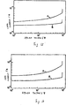
diodes 10 were constructed, each having a Ta-Ir amorphous contact barrier layer 1, with all other features of the diode having the same construction as in Embodiment 1. The relation between the Al content in the Ta-Ir amorphous contact barrier layer and the pn junction leakage current was investigated. The Ta-Ir amorphous contact barrier layers of the two diodes were respectively formed by sputtering using 48.5 wt% Ta-Ir composite targets respectively having Al concentrations of 100 and 30 ppm. When measured by frameless atomic absorption spectrophotometry, the Al contents of the respective layers were 8 x 1018cm-3 and 4 x 1017cm-3. The contact barrier layer thickness was about 90 nm in each diode. The measurement of leakage current was conducted in the same manner as in Embodiment 1. - The results of measurement of the pn junction leakage current values as a function of reverse bias voltage are shown in Figure 4. Curve A in Figure 4 shows the current-voltage characteristic of the diode having the Ta-Ir layer with an Al content of 8 x 1018cm-3 and Curve B shows the characteristic of the diode having the Ta-Ir layer with an Al content of 4 x 1017cm-3. In both Ta-Ir layers, the content of heavy metal elements other than Ta was low, i.e., below 1 x 1017cm-3 and the content of alkali metals was low, i.e., below 0.5 x 1016cm-3. As clearly seen from Figure 4, leakage current is suppressed substantially by reducing the Al content in the contact barrier layer.
- Two diodes were constructed, each having an Ni-Nb amorphous contact barrier layer 1, with all other features of the diode having the same construction as in Embodiment 1. The relation between the Al content in the Ni-Nb amorphous contact barrier layer and the pn junction leakage current was investigated. The Ni-Nb amorphous contact barrier layers of the two diodes were respectively formed using 61 wt% Ni-Nb composite targets with Al concentrations of 180 and 10 ppm, respectively. When measured by frameless atomic absorption spectrophotometry, the Al content in each Ni-Nb amorphous contact barrier layer was 1.5 x 1019cm-3 and 1 x 1017cm-3. The layer thickness was about 90 nm. The measurement of leakage current was conducted in the same manner as in Embodiment 1.
- The results of measurement of the pn junction leakage current value as a function of reverse bias voltage are shown in Figure 5. Curve A in Figure 5 shows the current-voltage characteristic of the diode having the Ni-Nb layer with an Al content of 1.5 x 1019cm-3 and Curve B shows the diode having the Ni-Nb layer with an Al content of 1 x 1017cm-3. In both Ni-Nb layers, the content of heavy metal elements other than Ni and Nb was low, i.e., below 1 x 1017cm-3 and the content of alkali metal was low, i.e., below 3 x 1016cm-3. As clearly seen from Figure 5, leakage current is suppressed substantially by reducing the Al content in the contact barrier layer.
- Two
diodes 10 were constructed, each having a Fe-W amorphous contact barrier layer 1, with all other features of the diode having the same construction as in Embodiment 1. The relation between the Al content in the Fe-W amorphous contact barrier layer and the pn junction leakage current was investigated. The Fe-W amorphous contact barrier layers of the two diodes were respectively formed by sputtering using 23.3 wt% Fe-W composite targets having Al concentrations of about 150 and 15 ppm, respectively. When measured by frameless atomic absorption spectrophotometry, the Al contents of the respective Fe-W amorphous contact barrier layers were 2.6 x 1018cm-3 and 1 x 1017cm-3. The contact barrier layer thickness was about 90 nm in each diode. The measurement of leakage current was conducted in the same manner as in Embodiment 1. - The results of measurement of the pn junction leakage current values as a function of reverse bias voltage are shown in Figure 6. Curve A in Figure 6 shows the current-voltage characteristic of the diode having the Fe-W layer with an Al content of 2.6 x 1018cm-3 and Curve B shows the characteristic of the diode having the Fe-W layer with an Al content of 1 x 1017cm-3. In both Fe-W layers, the content of heavy metal elements other than Fe and W was below 1 x 1017cm-3 and the content of alkali metal was below 0.5 x 1016cm-3. As clearly seen from Figure 6, leakage current is suppressed substantially by reducing the Al content in the contact barrier layer.
- Two
diodes 10 were constructed, each having a Ti silicide contact barrier layer 1, with all other features of the diode having the same construction as in Embodiment 1. The relation between the Al content in the Ti silicide contact barrier layer and the pn junction leakage current was investigated. The Ti silicide contact barrier layers of the two diodes were respectively formed according to the sputtering method using 56.0 wt% Ti-Si composite targets with Al concentrations of 150 and 15 ppm, respectively. - A Ti-Si composite target (Al content 150 ppm) was produced by the following process. A quantity of Ti made by the Kroll process was melted by arc discharge to form a Ti ingot of 140mm diameter. The Ti ingot was hot-forged, grinded, polished, and shaped to form a Ti sputtering target.
- Then Si-blocks (purity 5N) were uniformly spaced apart on the Ti target surface in a checkerboard-like mosaic pattern to cover approximately 56% of the area of the Ti target. The Al content in each Si-block was 1 ppm or less.
- A Ti-Si composite target (
Al content 10 ppm) was produced by the following process. An electrode made of sponge Ti was immersed into an electrolytic bath (KCl:16 wt%, NaCl: 84 wt%) and formed into Ti needles by the molten salt electrolysis method at conditions of 755°C, current 200A, and voltage 8V. - Then the Ti needles were washed in a NaOH solution, to remove Al on the surface of the needles, and rinsed in water. After that, the Ti needles were melted by the electron beam melting method under conditions of 5 x 10⁻⁵ mbar and 30kW and a Ti ingot of 135mm diameter was formed. The Ti ingot was cool-forged, grinded, polished, and shaped to form a Ti target.
- Then Si-blocks (purity 5N) were uniformly spaced apart on the Ti target surface in a checkerboard-like mosaic pattern to cover approximately 56% of the area of the Ti target. The Al content in each Si-block was 1 ppm or less.
- Using these targets (Al content 150 ppm, 10 ppm), the Ti silicide layers were produced by the sputtering method and the Al contents in the layers were 5 x 1018cm-3 and 1 x 1017cm-3, respectively, measured by frameless atomic absorption spectrophotometry. The layer thickness was about 90 nm in each diode. The measurement of leakage current was conducted in the same manner as in Embodiment 1.
- The results of measurement of the pn junction leakage current values as a function of reverse bias voltage are shown in Figure 7. Curve A in Figure 7 shows the current-voltage characteristic of the diode having the Ti silicide layer with an Al content of 5 x 1018cm-3 and Curve B shows the characteristic of the diode having the Ti silicide layer with an Al content of 1 x 1017cm-3. In both Ti-silicide layers, the content of heavy metal elements other than Ti was below 2 x 1017cm-3 and the content of alkali metals was below 1 x 1016cm-3. As clearly seen from Figure 7, leakage current is suppressed substantially by reducing the Al content in the contact barrier layer.
- Two
diodes 10 were constructed, each having a W-silicide contact barrier layer 1, with all other features of the diode having the same construction as in Embodiment 1. The relation between the Al content in the W-silicide contact barrier layer and the pn junction leakage current was investigated. The W-silicide contact barrier layers of the two diodes were respectively formed according to the sputtering method using 70.8 wt% W-Si composite targets having Al concentrations of about 150 and 0.3 ppm, respectively. - The W-silicide targets were produced by the following process.
- High purity W powder (maximum particle size of 10µm or less) was mixed for 48 hours with high purity Si powder (maximum particle size of 30µm or below) in the ratio of 70.8 wt% W-Si using a ballmill filled with high purity Ar gas.
- A BN mold release was spread on a surface of a mold made of graphite and a Ta-plate was put on the surface of the mold. Then the mold was filled with the mixed powder.
- Next, the mold was inserted in a hot-press machine and the mixed powder was changed to silicide under conditions of under 5 x 10⁻⁴ Torr, 1250°C for 2 hours, and pressure of 50 kg/cm2. Then the silicide was deoxidized and decarbonized under conditions of 135°C for 5 hours and was compacted and sintered under conditions of 1400°C for 5 hours and pressure of 270 kg/cm2 to form a sintered body.
- The sintered body was grinded, polished, and shaped by electrospark machining to form a first target of approximately 260mm diameter and 6mm thickness. The Al content in the first target was 0.3 ppm.
- Si powder (Al content 450 ppm) was mixed for 48 hours with high purity W powder (maximum particle size 10µm or less) in the ratio of 70.8 wt% W-Si using a ballmill filled with high purity Ar gas. Using this mixed powder, a second target was produced in a similar manner to that described above for producing the first target. The Al content of the second target was 150 ppm.
- When measured by frameless atomic absorption spectrophotometry, the Al contents of the respective W-silicide layers were 2.5 x 1018cm-3 and 1 x 1016cm-3, respectively. The layer thickness was about 90 nm in each diode. The measurement of leakage current was conducted in the same manner as in Embodiment 1.
- The results of measurement of the pn junction leakage current values of each diode as a function of the reverse bias voltage are shown in Figure 8. Curve A in Figure 8 shows the current-voltage characteristic of the diode having the W-silicide layer with an Al content of 2.5 x 1018cm-3 and Curve B shows the characteristic of the diode having the W-silicide layer with an Al content of 1 x 1016cm-3. In both W-silicide layers, the content of heavy metal elements other than W was low, i.e., below 1 x 1017cm-3 and the content of alkali metals was low, i.e., below 3 x 1016cm-3. As clearly seen from Figure 8, leakage current is suppressed substantially by reducing the Al content of the contact barrier layer.
- Two
diodes 10 were constructed, each having a Mo-silicide contact barrier layer 1, with all other features of the diode having the same construction as in Embodiment 1. The relation between the Al content in the Mo-silicide contact barrier layer and the pn junction leakage current was investigated. The Mo-silicide contact barrier layer was formed according to the sputtering method using 63.1 wt% No-Si composite targets having Al concentrations of about 150, 30 and 0.4 ppm, respectively. - The Mo-silicide targets were produced by the following process.
- High purity Mo powder (maximum particle size was 10µm or below) was mixed for 48 hours with high purity Si powder (maximum particle size of 30µm or below) in the ratio of 63.1 wt% Mo-Si using a ballmill filled with high purity Ar gas.
- A BN mold release was spread on a surface of a mold made of graphite and a Ta-plate was put on the surface of the mold. Then the mold was filled with the mixed powder.
- Next, the mold was inserted in a hot-press machine and the mixed powder was changed to silicide under conditions of under 5 x 10⁻⁴ Torr, 1100°C for 2 hours, and pressure of 40 kg/cm2. Then the silicide was deoxidized and decarbonized under conditions of 1350°C for 5 hours and was compacted and sintered under conditions of 1400°C for 5 hours and pressure of 280 kg/cm2 to form a sintered body.
- The sintered body was grinded, polished, and shaped by electrospark machining to form a first target of approximately 260mm diameter and 6mm thickness. The Al content in the first target was 0.4 ppm.
- Si powder (Al content 120 ppm for a second target) or Si powder (Al content 450 ppm for a third target) was mixed for 48 hours with high purity W powder (maximum particle size 10µm or below) in the ratio of 63.1 wt% Mo-Si using a ballmill filled with high purity Ar gas. Using these mixed powders, second and third targets were produced in a similar manner to that described above for the first target. The Al contents in the second and third targets were 150 ppm and 330 ppm, respectively.
- When measured by frameless atomic absorption spectrophotometry, the Al contents of the respective W-silicide layers were 2 x 1019cm-3 and 1 x 1018cm-3 and 1 x 1016cm-3, respectively. The layer thickness was about 90 nm in each diode. The measurement of leakage current was conducted in the same manner as in Embodiment 1.
- The results of measurement of the pn junction leakage current values of each diode as a function of the reverse bias voltage are shown in Figure 9. Curve A in Figure 9 shows the current-voltage characteristic of the diode having the W-silicide layer with an Al content of 2 x 1019cm-3, Curve B shows the characteristic of the diode having the W-silicide layer with an Al content of 1 x 1018cm-3, and Curve C shows the characteristic of the diode having the W-silicide layer with an Al content of 1 x 1016cm-3. In all three films, the content of heavy metal elements other than Mo was low, i.e., below 5 x 1016cm-3 and the content of alkali metals was below 5 x 1016cm-3. As clearly seen from Figure 9, leakage current is suppressed substantially by reducing the Al content of the contact barrier layer.
- Two
diodes 10 were constructed, each having a Ta-silicide contact barrier layer 1, with all other features of the diode having the same construction as in Embodiment 1. The relation between the Al content in the Ta-silicide contact barrier layer and the pn junction leakage current was investigated. The Ta-silicide contact barrier layers of the two diodes were respectively formed according to the sputtering method using 76.3 wt% Ta-Si composite targets having Al concentrations of about 150 ppm and 0.4 ppm, respectively. - The Ta-silicide targets were produced by the following process.
- High purity Ta powder (maximum particle size of 10µm or below) was mixed for 48 hours with high purity Si powder (maximum particle size of 30µm or below) in the ratio of 76.31 wt% Ta-Si using a ballmill filled with high purity Ar gas.
- A BN mold release was spread on a surface of a mold made of graphite and a Ta-plate was put on the surface of the mold. Then the mold was filled with the mixed powder.
- Next, the mold was inserted in a hot-press machine and the mixed powder was changed to silicide under conditions of under 5 x 10⁻⁴ Torr, 1150°C for 3 hours, and pressure of 60 kg/cm2. Then the silicide was deoxidized and decarbonized under conditions of 1300°C for 5 hours and was compacted and sintered under conditions of 1360°C for 5 hours and pressure of 280 kg/cm2 to form a sintered body.
- The sintered body was grinded, polished and shaped by electrospark machining to form a first target of approximately 260mm diameter and 6mm thickness. The Al content of the first target was 0.4 ppm.
- Si powder (Al content 430 ppm) was mixed for 48 hours with high purity Ta powder (maximum particle size 10µm or below) in the ratio of 76.3 wt% Ta-Si using a ballmill filled with high purity Ar gas. Using this mixed powder, a second target was produced in a similar manner to that described above. The Al content of the second target were 150 ppm.
- When measured by frameless atomic absorption spectrophotometry, the Al contents of the respective Ta-silicide layers were 4 x 1018cm-3 and 2 x 1017cm-3, respectively. The layer thickness was about 90 nm in each diode. The measurement of leakage current was conducted in the same manner as in Embodiment 1.
- The results of measurement of the pn junction leakage current values of each diode as a function of the reverse bias voltage are shown in Figure 10. Curve A in Figure 10 shows the current-voltage characteristic of the diode having the Ta-silicide layer with an Al content of 4 x 1018cm-3 and Curve B shows the characteristic of the diode having the Ta-silicide layer with an Al content of 2 x 1016cm-3. In both layers, the content of heavy metal elements other than Ta was low, i.e., below 2 x 1016cm-3 and the concentration of alkali metals was low, i.e., below 0.5 x 1016cm-3. As clearly seen from Figure 10, leakage current is suppressed substantially by reducing the Al content of the contact barrier layer.
- Two diodes were constructed, each having an Ni-silicide contact barrier layer 1, with all other features of the diode having the same construction as in Embodiment 1. The relation between the Al content in the Ni-silicide contact barrier layer and the pn junction leakage current was investigated. The Ni-silicide contact barrier layers of the two diodes were respectively formed according to the sputtering method using 51.1 wt% Ni-Si composite targets having Al concentrations of about 200 and 0.5 ppm, respectively.
- The Ni-silicide targets were produced by the following process.
- High purity Ni powder (maximum particle size of 10µm or less) was mixed for 48 hours with high purity Si powder (maximum particle size of 30µm or less) in the ratio of 51.1 wt% Ni-Si using a ballmill filled with high purity Ar gas.
- A BN mold release was spread on a surface of a mold made of graphite and a Ta-plate was put on the surface of the mold. Then the mold was filled with the mixed powder.
- Next, the mold was inserted in a hot-press machine and the mixed powder was changed to silicide under conditions of under 5 x 10⁻⁴ Torr, 750°C for 3 hours, and pressure of 50 kg/cm2. Then the silicide was deoxidized and decarbonized under conditions of 900°C for 5 hours and was compacted and sintered under conditions of 940°C for 5 hours and pressure of 280 kg/cm2 to form a sintered body.
- The sintered body was grinded, polished and shaped by electrospark machining to form a first target of approximately 260mm diameter and 6mm thickness. The Al content in the first target was 0.4 ppm.
- Si powder (Al content 400 ppm) was mixed for 48 hours with high purity Ni powder (maximum particle size 10µm or less) in the ratio of 51.1 wt% Ni-Si using a ballmill filled with high purity Ar gas. Using this mixed powder, a second target was produced in a similar manner to that described above for producing the first target. The Al content of the second target was 200 ppm.
- When measured by frameless atomic absorption spectrophotometry, the Al contents of the respective Ni-silicide layers were 8 x 1018cm-3 and 3 x 1016cm-3, respectively. The layer thickness was about 90 nm in each diode. The measurement of leakage current was conducted in the same manner as in Embodiment 1.
- The results of measurement of the pn junction leakage current values of each diode as a function of the reverse bias voltage are shown in Figure 11. Curve A in Figure 11 shows the current-voltage characteristic of the diode having the Ni-silicide layer with an Al content of 8 x 1018cm-3 and Curve B shows the characteristic of the diode having the Ni-silicide layer with an Al content of 3 x 1016cm-3. In both Ni-silicide layers, the content of heavy metal elements other than Ni was low, i.e., below 2 x 1017cm-3 and the content of alkali metals was low, i.e., below 1 x 1016cm-3. As clearly seen from Figure 11, leakage current is suppressed substantially by reducing the Al content of the contact barrier layer.
- Two
diodes 10 were constructed, each having a Co-silicide contact barrier layer 1, with all other features of the diode having the same construction as in Embodiment 1. The relation between the Al content in the Co-silicide contact barrier layer and the pn junction leakage current was investigated. The Co-silicide contact barrier layers of the two diodes were respectively formed according to the sputtering method using 51.2 wt% Co-Si composite targets having Al concentrations of about 200 and 0.6 ppm, respectively. - The Co-silicide targets were produced by the following process.
- High purity Co powder (maximum particle size of 10µm or less) was mixed for 48 hours with high purity Si powder (maximum particle size of 30µm or less) in the ratio of 51.2 wt% Co-Si using a ballmill filled with high purity Ar gas.
- A BN mold release was spread on a surface of a mold made of graphite and a Ta-plate was put on the surface of the mold. Then the mold was filled with the mixed powder.
- Next, the mold was inserted in a hot-press machine and the mixed powder was changed to silicide under conditions of under 5 x 10⁻⁴ Torr, 1000°C for 3 hours, and pressure of 40 kg/cm2. Then the silicide was deoxidized and decarbonized under conditions of 1150°C for 5 hours and was compacted and sintered under conditions of 1240°C for 5 hours and pressure of 280 kg/cm2 to form a sintered body.
- The sintered body was grinded, polished and shaped by electrospark machining to form a first target of approximately 260mm diameter and 6mm thickness. The Al content in the first target was 0.6 ppm.
- Si powder (Al content 320 ppm) was mixed for 48 hours with high purity Co powder (maximum particle size 10µm or less) in the ratio of 51.2 wt% Co-Si using a ballmill filled with high purity Ar gas. Using this mixed powder, a second target was produced in a similar manner to that described above for the first target. The Al content of the second target was 160 ppm.
- When measured by frameless atomic absorption spectrophotometry, the Al contents of the respective Co-silicide layers were 0.5 x 1019cm-3 and 2 x 1016cm-3, respectively. The layer thickness was about 80 nm in each diode. The measurement of leakage current was conducted in the same manner as in Embodiment 1.
- The results of measurement of the pn junction leakage current values of each diode as a function of the reverse bias voltage are shown in Figure 12. Curve A in Figure 12 shows the current-voltage characteristic of the diode having the Co-silicide layer with an Al content of 0.5 x 1019cm-3 and Curve B shows the characteristic of the diode having the Co-silicide layer with an Al content of 2 x 1016cm-3. In both Co-silicide layers, the content of heavy metal elements other than Co was low, i.e., below 2 x 1017cm-3 and the content of alkali metals was low, i.e., below 1 x 1016cm-3. As clearly seen from Figure 12, leakage current is suppressed substantially by reducing the Al content of the contact barrier layer.
- Three
diodes 10 were constructed, each having a Ti-nitride contact barrier layer 1, with all other features of the diode having the same construction as in Embodiment 1. The relation between the Al content in the Ti-nitride contact barrier layer and the pn junction leakage current was investigated. The Ti-nitride contact barrier layers of the three diodes were respectively formed according to the sputtering method in a nitrogen atmosphere using Ti targets having Al concentrations of about 150, 10, and 3, respectively. - A first Ti target (Al content 150 ppm) and a second Ti target (
Al content 10 ppm) were produced by the same method as described for embodiment 7. Each of these targets was machined to a circular shape approximately four inches in diameter. - A third Ti target (Al content 3 ppm) was produced in the following manner.
- The Ti needles were produced in the same way as described in embodiment 7.
- Then, the Ti needles were washed in a NaOH solution, to remove Al on the surfaces of the needles, and rinsed in water.
- Moreover, these needles were dipped for 3 minutes in a mixed solution consisting of hydrofluoric acid, nitric acid, hydrochloric acid and water (2:1:1:196 in wt%, respectively).
- After that, these Ti needles were melted by the electron beam melting method under the same conditions of embodiment 7 and a Ti ingot of 135mm diameter was formed. The Ti ingot was cool-forged and grinded, polished, and shaped to form a circular Ti target approximately four inches in diameter.
- Air in a chamber of a direct current dipole magnetron sputtering apparatus was evacuated to a pressure of 1 x 10⁻⁶ Torr. Next, the chamber was filled with a gas of 50% Ar-50% N2 at a pressure of 5 x 10⁻³ Torr. Then one of the Ti targets was placed in the chamber. The film was formed by sputtering of the target using a 400 watt direct current power supply.
- When measured by frameless atomic absorption spectrophotometry, the Al contents of the respective Ti-nitride layers were 1 x 1019cm-3, 1 x 1018cm-3 and 1 x 1017cm-3, respectively. Further, the layer thickness was about 100 nm in each diode. The measurement of leakage current was conducted in the same manner as in Embodiment 1.
- The results of measurement of the pn junction leakage current values of each diode as a function of the reverse bias voltage are shown in Figure 13. Curve A in Figure 13 shows the current-voltage characteristic of the diode having the Ti-nitride layer with an Al content of 1 x 1019cm-3, Curve B shows the characteristic of the diode having the Ti-nitride layer with an Al content of 1 x 1018cm-3, and Curve C shows the characteristic of the diode having the Ti-nitride layer with an Al content of 1 x 1017cm-3. In all Ti-nitride layers, the content of heavy metal elements other than Ti was low, i.e., below 5 x 1016cm-3 and the content of alkali metals was low, i.e., below 5 x 1016cm-3. As clearly seen from Figure 13, leakage current is suppressed substantially by reducing the Al content of the contact barrier layer.
- Two
diodes 10 were constructed, each having a Ta-nitride contact barrier layer 1, with all other features of the diode having the same construction as in Embodiment 1. The relation between the Al content in the Ta-nitride contact barrier layer and the pn junction leakage current was investigated. The Ta-nitride contact barrier layers of the two diodes were respectively formed in a nitrogen atmosphere according to the sputtering method using Ta targets having Al concentrations of about 150 and 1 ppm, respectively. - Sputtering was conducted as described above for
Embodiment 13, except that 350 watts of direct current power was used. - When measured by frameless atomic absorption spectrophotometry, the Al contents of the respective Ta-nitride contact barrier layers were 4 x 1018cm-3 and 1 x 1017cm-3, respectively. The layer thickness was about 80 nm in each diode. The measurement of leakage current was conducted in the same manner as in Embodiment 1.
- The results of measurement of the pn junction leakage current values of each diode as a function of reverse bias voltage are shown in Figure 14. Curve A in Figure 14 shows the current-voltage characteristic of the diode having the Ta-nitride layer with an Al content of 4 x 1018cm-3 and Curve B shows the characteristic of the diode having the Ta-nitride layer with an Al content of 1 x 1017cm-3. In both Ta-nitride layers, the content of heavy metal elements other than Ta was low, i.e., below 1 x 1017cm-3 and the content of alkali metals was low, i.e., below 3 x 1016cm-3. As clearly seen from Figure 14, leakage current is suppressed substantially by reducing the Al content in the contact barrier layer.
- Two
diodes 10 were constructed, each having a Ti-W nitride contact barrier layer 1, with all other features of the diode having the same construction as in Embodiment 1. The relation between the Al content in the Ti-W nitride contact barrier layer and the pn junction leakage current was investigated. The Ti-W nitride contact barrier layer was formed in a nitrogen atmosphere according to the sputtering method using 10 wt% Ti-W composite targets having Al concentrations of about 200 and 1 ppm, respectively. - Sputtering was conducted as described above for
Embodiment 13, except that 420 watts of direct current power was used. - When measured by frameless atomic absorption spectrophotometry, the Al contents of the respective Ti-W nitride layers were 5 x 1018cm-3 and 2 x 1017cm-3, respectively. The contact barrier layer thickness was about 80 nm in each diode. The measurement of leakage current was conducted in the same manner as in Embodiment 1.
- The results of measurement of the pn junction leakage current values of each diode as a function of reverse bias voltage are shown in Figure 15. Curve A in Figure 15 shows the current-voltage characteristic of the diode having the Ti-W nitride layer with an Al content of 5 x 1018cm-3 and Curve B shows the characteristic of the diode having the Ti-W nitride layer with an Al content of 2 x 1017cm-3. In both Ti-W nitride layers, the content of heavy metal elements other than Ti was low, i.e., below 2 x 1017cm-3 and the content of alkali metals was low, i.e., below 1 x 1016cm-3. As clearly seen from Figure 15, leakage current is suppressed substantially by reducing the Al content in the contact barrier layer.
- Two
diodes 10 were constructed, each having a W-nitride contact barrier layer 1, with all other features of the diode having the same construction as in Embodiment 1. The relation between the Al content in the W-nitride contact barrier layer and the pn junction leakage current was investigated. The W-nitride contact barrier layers of the two diodes were respectively formed in a nitrogen atmosphere according to the sputtering method using W targets having Al concentrations of about 170 and 1 ppm, respectively. - Sputtering was conducted as described above for
Embodiment 13, except that 450 watts of direct current power was used. - When measured by frameless atomic absorption spectrophotometry, the Al contents of the W-nitride contact barrier layers were 3 x 1018cm-3 and 1 x 1017cm-3, respectively. The layer thickness was about 90 nm in each diode. The measurement of leakage current was conducted in the same manner as in Embodiment 1.
- The results of measurement of the pn junction leakage current values of each diode as a function of reverse bias voltage are shown in Figure 16. Curve A in Figure 16 shows the current-voltage characteristic of the diode having the w-nitride layer with an Al content of 3 x 1018cm-3 and Curve B shows the characteristic of the diode having the W-nitride layer with an Al content of 1 x 1017cm-3. In both W-nitride layers, the content of heavy metal elements other than W was low, i.e., below 1 x 1017cm-3 and the content of alkali metals was low, i.e., below 1 x 1016cm-3. As clearly seen from Figure 16, leakage current is suppressed substantially by reducing the Al content in the contact barrier layer.
- Fig. 18 illustrates a MOSFET 20 having a conventional construction except for the composition of its gate electrode and contact barrier layers, which are constructed in accordance with the present invention. MOSFET 20 includes
substrate 22 of a first conductivity type. Asource area 24 and adrain area 26 are each of a second conductivity type, opposite the first conductivity type, and are diffused into a major surface ofsubstrate 22. An insulatingfilm 28 is deposited on the major surface ofsubstrate 22 and includesapertures source area 24 anddrain area 26. Contact barrier layers 34 and 36 are respectively deposited over the portions ofsource area 24 anddrain area 26 exposed byapertures Aluminum wires area 24 anddrain area 26. A gate electrode 42 is deposited over a portion of insulatingfilm 28 overlying the area between the source and drain areas. - In accordance with the present invention, gate electrode 42 and each of contact barrier layers 34 and 36 are composed of any one of the above described conductive film materials in which the aluminum content is maintained at or below 1 x 1018cm-3. As a result, the leakage current of MOSFET 20 can be kept at a nearly constant level as the device is down-sized, regardless of the depth of the source and drain areas.
- The present invention has been described with respect to specific embodiments. However, other embodiments based on the principles of the present invention should be obvious to those of ordinary skill in the art. Such embodiments are intended to be covered by the claims.
Claims (10)
- A semiconductor device including a contact barrier layer and/or a gate electrode either or both of which is constructed of high purity conductive film composed of conductive material whose impurity content of:
- A semiconductor device as claimed in claim 1 whose impurity content of (ii) heavy metals is < 1 x 1017 cm-3 and whose impurity content of (iii) alkali metals is < 5 x 1016 cm-3 in said gate electrode and/or contact barrier layer.
- A semiconductor device as claimed in either preceding claim including both contact barrier layer and gate electrode both of which are constructed from said conductive material.
- A semiconductor device as claimed in any preceding claim wherein the conductive material is composed of at least one kind of material comprising one or more of the following: Ti, W, Mo, Zr, Hf, Ta, V, Nb, Ir, Fe, Ni, Cr, Co, Pd and Pt.
- A semiconductor device as claimed in claim 4 wherein the said one kind of material is metallic silicide of one or more of the metallic elements defined in claim 4.
- A semiconductor device as claimed in claim 4 wherein the said one kind of material is nitride of one or more of the following: Ti, W, Ta, and alloys of Ti and W.
- A semiconductor device as claimed in any preceding claim comprising:wherein the contact barrier layer is composed of a second conductive material as defined in any preceding claim.a substrate of a first conductivity type and having a surface;a region of a second conductivity type opposite the first conductivity type and formed in the surface of the substrate;an insulating layer disposed on the surface of the substrate, the insulating layer including an aperture exposing at least a portion of the second conductivity type region;a contact barrier layer disposed on the portion of the second conductivity type region exposed by the aperture; anda contact layer composed of a first conductive material disposed at least on the contact barrier layer;
- A semiconductor device as claimed in any one of claims 1 to 6 further comprising:wherein the contact barrier layer and the electrode are each composed of conductive material as defined in any one of claims 1 to 6.a substrate of a first conductivity type and having a major surface;a source region of a second conductivity type opposite the first conductivity type and formed in the major surface of the substrate;a drain region of the second conductivity type formed in the major surface of the substrate at a location spaced apart from the source region;an insulating layer disposed on a portion of the major surface of the substrate, the insulating layer including apertures exposing at least a portion of the source region and a portion of the drain region;a contact barrier layer disposed on the respective portions of the source and drain regions exposed by the apertures;a contact layer composed of a first conductive material disposed at least on each contact barrier layer; andan electrode disposed on the insulating layer over a portion of the major surface of the substrate between the source and drain regions;
- A semiconductor device according to any preceding claim which is a diode.
- A semiconductor device according to any one of claims 1 to 8 which is a MOSFET device.
Applications Claiming Priority (3)
| Application Number | Priority Date | Filing Date | Title |
|---|---|---|---|
| JP797291 | 1991-01-25 | ||
| JP7972/91 | 1991-01-25 | ||
| JP797291 | 1991-01-25 |
Publications (3)
| Publication Number | Publication Date |
|---|---|
| EP0496637A2 EP0496637A2 (en) | 1992-07-29 |
| EP0496637A3 EP0496637A3 (en) | 1994-07-27 |
| EP0496637B1 true EP0496637B1 (en) | 2003-09-17 |
Family
ID=11680381
Family Applications (1)
| Application Number | Title | Priority Date | Filing Date |
|---|---|---|---|
| EP92300634A Expired - Lifetime EP0496637B1 (en) | 1991-01-25 | 1992-01-24 | High purity conductive films and their use in semiconductors |
Country Status (3)
| Country | Link |
|---|---|
| EP (1) | EP0496637B1 (en) |
| KR (1) | KR960007639B1 (en) |
| DE (1) | DE69233201T2 (en) |
Families Citing this family (3)
| Publication number | Priority date | Publication date | Assignee | Title |
|---|---|---|---|---|
| JPH05214523A (en) * | 1992-02-05 | 1993-08-24 | Toshiba Corp | Sputtering target and its manufacture |
| WO2000029636A2 (en) * | 1998-11-12 | 2000-05-25 | Applied Materials, Inc. | High purity tantalum targets for sputtering |
| CN102197155B (en) | 2009-04-17 | 2013-07-17 | 吉坤日矿日石金属株式会社 | Barrier film for semiconductor wiring, sintered sputtering target, and method for producing sputtering target |
Family Cites Families (6)
| Publication number | Priority date | Publication date | Assignee | Title |
|---|---|---|---|---|
| JPS5838942B2 (en) * | 1975-08-28 | 1983-08-26 | 三菱電機株式会社 | ShyotsutoshiyouhekigatahandoutaisouchiOyobiSonoseizohou |
| FR2530383A1 (en) * | 1982-07-13 | 1984-01-20 | Thomson Csf | MONOLITHIC INTEGRATED CIRCUIT COMPRISING A SCHOTTKY LOGIC PART AND A PROGRAMMABLE FUSE MEMORY |
| JPS60154614A (en) * | 1984-01-25 | 1985-08-14 | Hitachi Ltd | Formation of metal silicide electrode |
| JPS63227771A (en) * | 1987-03-16 | 1988-09-22 | Tosoh Corp | High purity titanium silicide target for sputtering and production thereof |
| JP2941828B2 (en) * | 1988-12-21 | 1999-08-30 | 株式会社東芝 | Refractory metal silicide target and method for producing the same |
| JPH02302042A (en) * | 1989-05-16 | 1990-12-14 | Sharp Corp | Manufacture of semiconductor device |
-
1992
- 1992-01-24 DE DE69233201T patent/DE69233201T2/en not_active Expired - Lifetime
- 1992-01-24 EP EP92300634A patent/EP0496637B1/en not_active Expired - Lifetime
- 1992-01-25 KR KR1019920001114A patent/KR960007639B1/en not_active Expired - Lifetime
Also Published As
| Publication number | Publication date |
|---|---|
| EP0496637A3 (en) | 1994-07-27 |
| EP0496637A2 (en) | 1992-07-29 |
| DE69233201T2 (en) | 2004-07-01 |
| KR960007639B1 (en) | 1996-06-07 |
| DE69233201D1 (en) | 2003-10-23 |
| KR920015467A (en) | 1992-08-26 |
Similar Documents
| Publication | Publication Date | Title |
|---|---|---|
| KR940008936B1 (en) | Highly purified metal material and sputtering target using the same | |
| TWI413252B (en) | A wiring structure, a thin film transistor substrate, a method of manufacturing the same, and a display device | |
| Suni et al. | Performance of titanium nitride diffusion barriers in aluminum–titanium metallization schemes for integrated circuits | |
| Wang et al. | Formation of aluminum oxynitride diffusion barriers for Ag metallization | |
| EP0458353B1 (en) | Ohmic contact electrodes for n-type semiconductor cubic boron nitride | |
| US8262816B2 (en) | Hafnium alloy target | |
| Mehrotra et al. | Properties of direct current magnetron reactively sputtered TaN | |
| JPH081896B2 (en) | Contact structure for gallium arsenide and method for producing the same | |
| US5436505A (en) | Heat-resisting ohmic contact on semiconductor diamond layer | |
| KR20030020986A (en) | Sputtering target | |
| US20110287626A1 (en) | Ohmic electrode and method of forming the same | |
| EP0496637A2 (en) | High purity conductive films and their use in semiconductors | |
| US6187667B1 (en) | Method of forming metal layer(s) and/or antireflective coating layer(s) on an integrated circuit | |
| Schutz | TiN as a diffusion barrier between CoSi2 or PtSi and aluminum | |
| JP3609682B2 (en) | Manufacturing method of semiconductor device | |
| JP3330938B2 (en) | Stabilization of the interface between aluminum and titanium nitride | |
| JP3398611B2 (en) | High-purity conductive film for semiconductor device and semiconductor device using the same | |
| JP3021900B2 (en) | High purity conductive film for semiconductor device, semiconductor device using the same, and method of forming high purity conductive film for semiconductor device | |
| JPH05291560A (en) | Barrier metal for semiconductor devices | |
| JP2707305B2 (en) | Thin film forming method, semiconductor device obtained by the method, and method of manufacturing the same | |
| EP0260232B1 (en) | Process for making metal-semiconductor ohmic contacts | |
| JP4496374B2 (en) | Target made of high purity Ta material | |
| JP4496371B2 (en) | Manufacturing method of semiconductor device | |
| JP4543011B2 (en) | Target made of high purity W silicide material | |
| JP3923058B2 (en) | Manufacturing method of semiconductor device |
Legal Events
| Date | Code | Title | Description |
|---|---|---|---|
| PUAI | Public reference made under article 153(3) epc to a published international application that has entered the european phase |
Free format text: ORIGINAL CODE: 0009012 |
|
| 17P | Request for examination filed |
Effective date: 19920207 |
|
| AK | Designated contracting states |
Kind code of ref document: A2 Designated state(s): DE FR GB |
|
| PUAL | Search report despatched |
Free format text: ORIGINAL CODE: 0009013 |
|
| AK | Designated contracting states |
Kind code of ref document: A3 Designated state(s): DE FR GB |
|
| 17Q | First examination report despatched |
Effective date: 19960318 |
|
| APAB | Appeal dossier modified |
Free format text: ORIGINAL CODE: EPIDOS NOAPE |
|
| APAB | Appeal dossier modified |
Free format text: ORIGINAL CODE: EPIDOS NOAPE |
|
| APAD | Appeal reference recorded |
Free format text: ORIGINAL CODE: EPIDOS REFNE |
|
| APAD | Appeal reference recorded |
Free format text: ORIGINAL CODE: EPIDOS REFNE |
|
| GRAH | Despatch of communication of intention to grant a patent |
Free format text: ORIGINAL CODE: EPIDOS IGRA |
|
| RIC1 | Information provided on ipc code assigned before grant |
Free format text: 7H 01L 29/47 A |
|
| GRAH | Despatch of communication of intention to grant a patent |
Free format text: ORIGINAL CODE: EPIDOS IGRA |
|
| GRAA | (expected) grant |
Free format text: ORIGINAL CODE: 0009210 |
|
| AK | Designated contracting states |
Kind code of ref document: B1 Designated state(s): DE FR GB |
|
| REG | Reference to a national code |
Ref country code: GB Ref legal event code: FG4D |
|
| REF | Corresponds to: |
Ref document number: 69233201 Country of ref document: DE Date of ref document: 20031023 Kind code of ref document: P |
|
| ET | Fr: translation filed | ||
| PLBE | No opposition filed within time limit |
Free format text: ORIGINAL CODE: 0009261 |
|
| 26N | No opposition filed |
Effective date: 20040618 |
|
| APAH | Appeal reference modified |
Free format text: ORIGINAL CODE: EPIDOSCREFNO |
|
| PGFP | Annual fee paid to national office [announced via postgrant information from national office to epo] |
Ref country code: FR Payment date: 20110128 Year of fee payment: 20 Ref country code: DE Payment date: 20110119 Year of fee payment: 20 |
|
| PGFP | Annual fee paid to national office [announced via postgrant information from national office to epo] |
Ref country code: GB Payment date: 20110119 Year of fee payment: 20 |
|
| REG | Reference to a national code |
Ref country code: DE Ref legal event code: R071 Ref document number: 69233201 Country of ref document: DE |
|
| REG | Reference to a national code |
Ref country code: DE Ref legal event code: R071 Ref document number: 69233201 Country of ref document: DE |
|
| REG | Reference to a national code |
Ref country code: GB Ref legal event code: PE20 Expiry date: 20120123 |
|
| PG25 | Lapsed in a contracting state [announced via postgrant information from national office to epo] |
Ref country code: DE Free format text: LAPSE BECAUSE OF EXPIRATION OF PROTECTION Effective date: 20120125 |
|
| PG25 | Lapsed in a contracting state [announced via postgrant information from national office to epo] |
Ref country code: GB Free format text: LAPSE BECAUSE OF EXPIRATION OF PROTECTION Effective date: 20120123 |