EP0490324B1 - Cutting system - Google Patents
Cutting system Download PDFInfo
- Publication number
- EP0490324B1 EP0490324B1 EP91121103A EP91121103A EP0490324B1 EP 0490324 B1 EP0490324 B1 EP 0490324B1 EP 91121103 A EP91121103 A EP 91121103A EP 91121103 A EP91121103 A EP 91121103A EP 0490324 B1 EP0490324 B1 EP 0490324B1
- Authority
- EP
- European Patent Office
- Prior art keywords
- cutting
- detecting means
- detecting
- wafers
- stroke
- Prior art date
- Legal status (The legal status is an assumption and is not a legal conclusion. Google has not performed a legal analysis and makes no representation as to the accuracy of the status listed.)
- Expired - Lifetime
Links
Images



Classifications
-
- H—ELECTRICITY
- H10—SEMICONDUCTOR DEVICES; ELECTRIC SOLID-STATE DEVICES NOT OTHERWISE PROVIDED FOR
- H10P—GENERIC PROCESSES OR APPARATUS FOR THE MANUFACTURE OR TREATMENT OF DEVICES COVERED BY CLASS H10
- H10P72/00—Handling or holding of wafers, substrates or devices during manufacture or treatment thereof
- H10P72/04—Apparatus for manufacture or treatment
- H10P72/0428—Apparatus for mechanical treatment or grinding or cutting
-
- B—PERFORMING OPERATIONS; TRANSPORTING
- B27—WORKING OR PRESERVING WOOD OR SIMILAR MATERIAL; NAILING OR STAPLING MACHINES IN GENERAL
- B27B—SAWS FOR WOOD OR SIMILAR MATERIAL; COMPONENTS OR ACCESSORIES THEREFOR
- B27B31/00—Arrangements for conveying, loading, turning, adjusting, or discharging the log or timber, specially designed for saw mills or sawing machines
- B27B31/06—Adjusting equipment, e.g. using optical projection
-
- B—PERFORMING OPERATIONS; TRANSPORTING
- B28—WORKING CEMENT, CLAY, OR STONE
- B28D—WORKING STONE OR STONE-LIKE MATERIALS
- B28D5/00—Fine working of gems, jewels, crystals, e.g. of semiconductor material; apparatus or devices therefor
- B28D5/0058—Accessories specially adapted for use with machines for fine working of gems, jewels, crystals, e.g. of semiconductor material
- B28D5/0064—Devices for the automatic drive or the program control of the machines
-
- B—PERFORMING OPERATIONS; TRANSPORTING
- B28—WORKING CEMENT, CLAY, OR STONE
- B28D—WORKING STONE OR STONE-LIKE MATERIALS
- B28D5/00—Fine working of gems, jewels, crystals, e.g. of semiconductor material; apparatus or devices therefor
- B28D5/0058—Accessories specially adapted for use with machines for fine working of gems, jewels, crystals, e.g. of semiconductor material
- B28D5/0082—Accessories specially adapted for use with machines for fine working of gems, jewels, crystals, e.g. of semiconductor material for supporting, holding, feeding, conveying or discharging work
-
- B—PERFORMING OPERATIONS; TRANSPORTING
- B28—WORKING CEMENT, CLAY, OR STONE
- B28D—WORKING STONE OR STONE-LIKE MATERIALS
- B28D5/00—Fine working of gems, jewels, crystals, e.g. of semiconductor material; apparatus or devices therefor
- B28D5/02—Fine working of gems, jewels, crystals, e.g. of semiconductor material; apparatus or devices therefor by rotary tools, e.g. drills
- B28D5/022—Fine working of gems, jewels, crystals, e.g. of semiconductor material; apparatus or devices therefor by rotary tools, e.g. drills by cutting with discs or wheels
-
- H—ELECTRICITY
- H10—SEMICONDUCTOR DEVICES; ELECTRIC SOLID-STATE DEVICES NOT OTHERWISE PROVIDED FOR
- H10P—GENERIC PROCESSES OR APPARATUS FOR THE MANUFACTURE OR TREATMENT OF DEVICES COVERED BY CLASS H10
- H10P72/00—Handling or holding of wafers, substrates or devices during manufacture or treatment thereof
- H10P72/06—Apparatus for monitoring, sorting, marking, testing or measuring
- H10P72/0606—Position monitoring, e.g. misposition detection or presence detection
-
- H—ELECTRICITY
- H10—SEMICONDUCTOR DEVICES; ELECTRIC SOLID-STATE DEVICES NOT OTHERWISE PROVIDED FOR
- H10P—GENERIC PROCESSES OR APPARATUS FOR THE MANUFACTURE OR TREATMENT OF DEVICES COVERED BY CLASS H10
- H10P72/00—Handling or holding of wafers, substrates or devices during manufacture or treatment thereof
- H10P72/50—Handling or holding of wafers, substrates or devices during manufacture or treatment thereof for positioning, orientation or alignment
- H10P72/53—Handling or holding of wafers, substrates or devices during manufacture or treatment thereof for positioning, orientation or alignment using optical controlling means
-
- H—ELECTRICITY
- H10—SEMICONDUCTOR DEVICES; ELECTRIC SOLID-STATE DEVICES NOT OTHERWISE PROVIDED FOR
- H10P—GENERIC PROCESSES OR APPARATUS FOR THE MANUFACTURE OR TREATMENT OF DEVICES COVERED BY CLASS H10
- H10P72/00—Handling or holding of wafers, substrates or devices during manufacture or treatment thereof
- H10P72/70—Handling or holding of wafers, substrates or devices during manufacture or treatment thereof for supporting or gripping
- H10P72/76—Handling or holding of wafers, substrates or devices during manufacture or treatment thereof for supporting or gripping using mechanical means, e.g. clamps or pinches
- H10P72/7604—Handling or holding of wafers, substrates or devices during manufacture or treatment thereof for supporting or gripping using mechanical means, e.g. clamps or pinches the wafers being placed on a susceptor, stage or support
- H10P72/7621—Handling or holding of wafers, substrates or devices during manufacture or treatment thereof for supporting or gripping using mechanical means, e.g. clamps or pinches the wafers being placed on a susceptor, stage or support characterised by supporting two or more semiconductor substrates
Definitions
- the present invention relates to a cutting system for detecting the size, shape, and position of a workpiece and suitably cutting the workpiece according to the detected information
- a cutting system is including a dicing system for holding indeterminate-shape or disorderly semiconductor wafers with a specified frame, suitably aligning the wafers according to the detected information, and suitably cutting them with a specified blade installed .
- An aligning system for dicing (cutting) a workpiece such as a semiconductor wafer consisting of the structure disclosed in the official gazette of for example, Japanese Patent Laid-open Publication No. 60-244803 is generally known as an embodiment according to the prior art.
- semiconductor wafers with regular size and shape such as those with the diameter of 125 mm (5") or 150 mm (6") are properly held by a frame respectively and provided with pattern matching and alignment at the pixel density of the X-Y-axis matrix caught by a camera according to the optimum alignment stroke previously set to said wafer with regular size.
- alignment can automatically be executed only when wafers have regular size and shape, and one wafer is properly held by one frame.
- workpieces of the same type with different sizes e.g. 5" and 6
- the embodiment according to the prior art has the problem to be solved in automatically dicing disorderly wafers of different shapes in order to improve operability.
- the present invention provides a cutting cutting method and cutting apparatus as outlined in the claims.
- the size, shape, quantity, and position of the wafers mounted on a frame are detected by the first detecting means on an X-Y-axis matrix (e.g. X-Y-axis matrix consisting of 256x256 pixels of a CCD camera), the detected information is stored as data on a memory, each wafer is accurately aligned by the second detecting means according to the data, the cutting stroke is specified at the same time, therefore wafers with different sizes and shapes, for which it is impossible to be aligned by the conventional pattern matching, are automatically and suitably cut (diced).
- X-Y-axis matrix e.g. X-Y-axis matrix consisting of 256x256 pixels of a CCD camera
- numeral 1 is a control section including a storage section.
- the control section 1 controls the first detecting means 2, second detecting means 3, and cutting means 8.
- the first detecting means 1 is installed at the first detecting position 4 and the second detecting means 3 is installed at the second detecting position 5.
- the size, shape, position, and quantity of wafers 6 are detected.
- wafers are accurately aligned to be cut.
- a CCD camera consisting of 256x256 pixels is used as these detecting means.
- the wafer 6 is held on the specified holding means such as a base or table 7 and cut by the specified cutting means, i.e. the blade 8 in the cutting area A according to the data consisting of the information by the detecting means.
- Numeral 10 is a film for mounting wafers.
- the frame 9 having the wafers 6a, 6b and 6c is entirely picked up by the first detecting means 2 at the first detecting position 4 to detect the wafer state.
- the size, shape, and quantity of wafers mounted on the frame 9 are detected on the X-Y-axis matrix.
- approximate tilt angle " ⁇ " of the cutting street is detected by the known means as shown in the official gazette of Japanese Patent Laid-open Publication No. 60-54454 according to necessity and further the position of the wafers 6a, 6b and 6c on the X-Y-axis matrix are detected.
- the information for the alignment stroke and cutting stroke according to the above-mentioned are stored in the control section 1.
- the wafers 6a, 6b and 6c are accurately aligned at their positions by the known pattern-matching means as shown in the above-mentioned prior art according to the information obtained at the first detecting position 4, and alignment information is detected.
- steps are comprising, for example, detecting accurately how the displacement and tilt angle on the X-Y-axis of the cutting streets "a" and "b" of the wafer 6a on the frame 9 are, storing such data as information, also detecting the cutting strokes of the cutting means 8 in the X-axis direction as shown in Fig. 3 and the Y-axis direction as shown in Fig. 4 according to the size and shape of the wafer 6a based on the information obtained at the first detecting means, and storing the both detected informations in the control section 1. Similarly, the displacement, tilt angle and cutting stroke of other wafers 6b and 6c are detected and stored in the control section 1.
- the first detecting means 2 may be formed as an independent unit or installed in other unit.
- the first detecting means may be installed in a unit for mounting the wafers on the frame 9, so-called wafer mounting unit, or installed in the dicing unit together with or separately from the second detecting means 3.
- the first and second detecting means are integrated as a detecting means 11.
- a CCD camera similarly to the above-mentioned may be used as the detecting means 11.
- the size and shape of the wafers mounted on the frame 9 and the position of each wafer on the X-Y-axis matrix are detected and are stored in the control section 1 as information.
- the frame 9 is mounted on a base or table 7 and wafers are suitably cut by the cutting means 8 in the cutting area A, similarly to the procedure for the above embodiment.
- the size, shape, position, quantity and cutting street of one or more wafers mounted on the frame 9 are detected on the X-Y-axis matrix, and, at the same time, the cutting stroke is also detected corresponding to the size and shape of the wafers. Accordingly, cutting (dicing) is accurately and securely executed according to these pieces of information.
- the first step a one or more wafers mounted on the frame 9 are supplied to the first position 4 of the first detecting means 2.
- the state of the wafer is detected by the first detecting means 2 at the first position 4. That is, the size, shape, position, and tilt angle of the cutting street of the wafers corresponding to the X-Y-axis matrix are detected as information.
- the optimum alignment stroke and cutting stroke of the wafers are calculated according to the detected information for the size, shape, position and tilt angle of cutting street corresponding to the X-Y-axis matrix.
- the data detected in the second step b and calculated in the third step c is transferred to and stored in the control section 1 as information.
- each wafer on the frame is accurately aligned by the second detecting means 3, e.g. pattern matching means with the optimum alignment stroke according to the information in the first detecting means 2 and the alignment information is stored in the control section 1.
- the wafers are cut at the cutting area A according to the cutting-stroke information obtained by the first detecting means 2 and stored in the control section 1 and the alignment information obtained by the second detecting means 3 and stored in the control section 1.
- the cut wafers are cleaned after the end of the dicing process and the frames having the cleaned wafers are delivered to the next process.
- the second step b through the fifth step e are executed by one detecting means 11 made by integrating the first and second detecting means and the sixth f and seventh g steps are executed in order according to the data detected by the detecting means 11.
- the above steps are repeated every supplied frame. Therefore, suitable dicing can continuously be executed even if the size, shape, and quantity (one or more) of wafers mounted on each frame are different.
- a CCD camera is used as detecting means, however, the detecting means is not limited, e.g. various types of detecting means including ultrasonic detecting means, laser beam detecting means and so on may be used.
- the size, shape, and position of a workpiece are detected by the ultrasonic or laser-beam detecting means as shown in Figs. 7 through 9.
- the size, shape and position of the wafer 6d are detected by detecting the level difference "h" between the wafer 6d and the holding means 10a for holding the wafer according to scanning them by the detecting means or detecting the difference of reflected luminous energy (Figs. 7 and 8) and plotting the boundary points (e1, e2,..., and en) between the wafer 6d and the holding means 10a on the X-Y coordinate axis (X-Y-axis matrix) (Fig. 9). Then, cutting is executed.
- the cutting and dicing system of the present invention comprises a frame for holding wafers, first detecting means for detecting the size, shape and position of the wafer held by the frame on an X-Y-axis matrix, second detecting means for aligning the wafers according to the information detected by the first detecting means, and cutting means for cutting the wafers according to the information detected by the second detecting means, wherein the size, shape and position of indeterminate-shape and disorderly wafers are detected by the first detecting means on an X-Y-axis matrix, the wafers are accurately aligned by the second detecting means according to the detected information, and one or more indeterminate-shape wafers are automatically and accurately diced though they are only manually diced conventionally.
- the first detecting means detects the size, shape and position of a wafer on an X-Y-axis matrix and the cutting stroke is controlled according to the information detected by the first detecting means. Accordingly, it is confirmed that the cutting efficiency is improved and the throughput is increased up to 1.5 times compared with the conventional throughput. Even if a plurality of wafers are mounted on one frame, each wafer can be cut (diced) without moving unnecessarily and being affected by other wafers.
- the second detecting means and cutting means in the same unit, the first detecting means, independently or in other unit, or the first detecting means, second detecting means and cutting means in the same unit. It is also possible to make the first and second detecting means common. Accordingly, it is possible to simply upgrade the conventional dicing systems.
Landscapes
- Engineering & Computer Science (AREA)
- Mechanical Engineering (AREA)
- Life Sciences & Earth Sciences (AREA)
- Wood Science & Technology (AREA)
- Forests & Forestry (AREA)
- Dicing (AREA)
- Processing Of Stones Or Stones Resemblance Materials (AREA)
- Container, Conveyance, Adherence, Positioning, Of Wafer (AREA)
- Machine Tool Sensing Apparatuses (AREA)
Description
- The present invention relates to a cutting system for detecting the size, shape, and position of a workpiece and suitably cutting the workpiece according to the detected information, particularly, a cutting system is including a dicing system for holding indeterminate-shape or disorderly semiconductor wafers with a specified frame, suitably aligning the wafers according to the detected information, and suitably cutting them with a specified blade installed .
- An aligning system for dicing (cutting) a workpiece such as a semiconductor wafer consisting of the structure disclosed in the official gazette of for example, Japanese Patent Laid-open Publication No. 60-244803 is generally known as an embodiment according to the prior art.
- For the above invention according to the prior art, semiconductor wafers with regular size and shape such as those with the diameter of 125 mm (5") or 150 mm (6") are properly held by a frame respectively and provided with pattern matching and alignment at the pixel density of the X-Y-axis matrix caught by a camera according to the optimum alignment stroke previously set to said wafer with regular size.
- For dicing, alignment is necessary to accurately align the cutting line (street) of a semiconductor wafer with the blade for cutting the wafer. To improve the alignment accuracy, it is necessary to execute pattern matching at two separate places (alignment stroke) on a wafer. In a conventional method, for an indeterminate-shape wafer such as a broken wafer, pattern matching may not be executed within the alignment stroke. In this case, it is necessary to change the alignment stroke manually. When a plurality of wafers are present on a frame, it is necessary to set the alignment stroke every wafer.
- Therefore, for the above embodiment according to the prior art, alignment can automatically be executed only when wafers have regular size and shape, and one wafer is properly held by one frame. However, if workpieces of the same type with different sizes (e.g. 5" and 6") are supplied to a production line, it is necessary to manually select the condition meeting each workpiece. In this case, selection of condition greatly decreases the efficiency of continuous automatic operation.
- In addition, in order to prevent expensive wafers from wasting, partially broken wafers are formed into chips by separating usable portions from unusable ones. In this case, however, automatic cutting is impossible. Therefore, manual alignment is executed before cutting. Especially when a plurality of indeterminate-shape and disorderly wafers are held by one frame, it is impossible to automatically align and cut individual wafer.
- Therefore, the embodiment according to the prior art has the problem to be solved in automatically dicing disorderly wafers of different shapes in order to improve operability.
- In order to solve the problem of the embodiment according to the prior art, the present invention provides a cutting cutting method and cutting apparatus as outlined in the claims.
- The size, shape, quantity, and position of the wafers mounted on a frame are detected by the first detecting means on an X-Y-axis matrix (e.g. X-Y-axis matrix consisting of 256x256 pixels of a CCD camera), the detected information is stored as data on a memory, each wafer is accurately aligned by the second detecting means according to the data, the cutting stroke is specified at the same time, therefore wafers with different sizes and shapes, for which it is impossible to be aligned by the conventional pattern matching, are automatically and suitably cut (diced).
-
- Fig. 1 is an explanatory drawing schematically showing the first embodiment of the dicing system of the present invention;
- Fig. 2 is a top view of the frame having a plurality of indeterminate-shape and disorderly wafers;
- Fig. 3 is an explanatory drawing showing the X-directional cutting stroke for a wafer;
- Fig. 4 is an explanatory drawing showing the Y-directional cutting stroke for a wafer;
- Fig. 5 is an explanatory drawing schematically showing the second embodiment of the dicing system of the present invention;
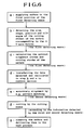
- Fig. 6 is a flow chart showing the dicing step of the dicing system of the present invention;
- Fig. 7 is an explanatory drawing showing another embodiment of the workpiece detecting means applicable to the cutting and dicing system of the present invention;
- Fig. 8 is an explanatory drawing for detection according to level difference detected by the detecting means of another embodiment shown in Fig. 7; and
- Fig. 9 is a graph for explaining plotting of positions by the level difference detected by the detecting means of another embodiment shown in Fig. 7.
-
- 1 :
- Control section
- 2 :
- First detecting means
- 3 :
- Second detecting means including an alignment means
- 4 :
- First position
- 5 :
- Second position
- 6, 6a, 6b, 6c:
- Wafer
- 6d:
- Workpiece
- 7 :
- Base or table
- 8 :
- Cutting means
- 9 :
- Frame
- 10 :
- Film
- 10a:
- Holding means
- 11 :
- Detecting means
- A :
- Cutting area
- In the embodiment shown in Fig. 1,
numeral 1 is a control section including a storage section. Thecontrol section 1 controls the first detecting means 2, second detecting means 3, and cutting means 8. The first detectingmeans 1 is installed at the first detecting position 4 and the second detectingmeans 3 is installed at the second detectingposition 5. At the first detecting position, the size, shape, position, and quantity ofwafers 6 are detected. At the second detecting position, wafers are accurately aligned to be cut. For example, a CCD camera consisting of 256x256 pixels is used as these detecting means. Thewafer 6 is held on the specified holding means such as a base or table 7 and cut by the specified cutting means, i.e. theblade 8 in the cutting area A according to the data consisting of the information by the detecting means. - For the
wafer 6, as shown in Fig. 2, for example, three wafers of 6a, 6b, and 6c are mounted on aframe 9. These wafers are partially chipped and their shapes and sizes are disorderly and indeterminate, which are mounted on the frame by visually arranging the cutting streets "a" and "b" of each wafer.Numeral 10 is a film for mounting wafers. - The
frame 9 having thewafers means 2 at the first detecting position 4 to detect the wafer state. In this case, the size, shape, and quantity of wafers mounted on theframe 9 are detected on the X-Y-axis matrix. In addition, approximate tilt angle "Θ" of the cutting street is detected by the known means as shown in the official gazette of Japanese Patent Laid-open Publication No. 60-54454 according to necessity and further the position of thewafers control section 1. - At the second detecting
position 5, thewafers - That is, such steps are comprising, for example, detecting accurately how the displacement and tilt angle on the X-Y-axis of the cutting streets "a" and "b" of the
wafer 6a on theframe 9 are, storing such data as information, also detecting the cutting strokes of the cutting means 8 in the X-axis direction as shown in Fig. 3 and the Y-axis direction as shown in Fig. 4 according to the size and shape of thewafer 6a based on the information obtained at the first detecting means, and storing the both detected informations in thecontrol section 1. Similarly, the displacement, tilt angle and cutting stroke ofother wafers control section 1. - The first detecting
means 2 may be formed as an independent unit or installed in other unit. For example, the first detecting means may be installed in a unit for mounting the wafers on theframe 9, so-called wafer mounting unit, or installed in the dicing unit together with or separately from the second detectingmeans 3. - The above example is shown in Fig. 5. That is, the first and second detecting means are integrated as a detecting
means 11. A CCD camera similarly to the above-mentioned may be used as the detectingmeans 11. Then, the size and shape of the wafers mounted on theframe 9 and the position of each wafer on the X-Y-axis matrix (e.g. matrix consisting of 256x256 pixels of a CCD camera) are detected and are stored in thecontrol section 1 as information. - At the same time, the tilt angle of the cutting street of each wafer on the X-Y-axis matrix is detected and the cutting stroke is also detected corresponding to the size and shape of each wafer. These pieces of information are stored in the
control section 1. Theframe 9 is mounted on a base or table 7 and wafers are suitably cut by the cutting means 8 in the cutting area A, similarly to the procedure for the above embodiment. - For the above embodiment, the size, shape, position, quantity and cutting street of one or more wafers mounted on the
frame 9 are detected on the X-Y-axis matrix, and, at the same time, the cutting stroke is also detected corresponding to the size and shape of the wafers. Accordingly, cutting (dicing) is accurately and securely executed according to these pieces of information. - The following is the description of dicing for the system of the present invention according to the flow chart in Fig. 6. In the first step a , one or more wafers mounted on the
frame 9 are supplied to the first position 4 of the first detectingmeans 2. In the second step b , the state of the wafer is detected by the first detectingmeans 2 at the first position 4. That is, the size, shape, position, and tilt angle of the cutting street of the wafers corresponding to the X-Y-axis matrix are detected as information. - In the third step c , the optimum alignment stroke and cutting stroke of the wafers are calculated according to the detected information for the size, shape, position and tilt angle of cutting street corresponding to the X-Y-axis matrix. In the fourth step d , the data detected in the second step b and calculated in the third step c is transferred to and stored in the
control section 1 as information. - In the fifth step e , each wafer on the frame is accurately aligned by the second detecting
means 3, e.g. pattern matching means with the optimum alignment stroke according to the information in the first detectingmeans 2 and the alignment information is stored in thecontrol section 1. In the sixth step f , the wafers are cut at the cutting area A according to the cutting-stroke information obtained by the first detectingmeans 2 and stored in thecontrol section 1 and the alignment information obtained by the second detectingmeans 3 and stored in thecontrol section 1. And in the seventh step g , the cut wafers are cleaned after the end of the dicing process and the frames having the cleaned wafers are delivered to the next process. - The second step b through the fifth step e are executed by one detecting means 11 made by integrating the first and second detecting means and the sixth f and seventh g steps are executed in order according to the data detected by the detecting
means 11. The above steps are repeated every supplied frame. Therefore, suitable dicing can continuously be executed even if the size, shape, and quantity (one or more) of wafers mounted on each frame are different. - In the above embodiment, a CCD camera is used as detecting means, however, the detecting means is not limited, e.g. various types of detecting means including ultrasonic detecting means, laser beam detecting means and so on may be used.
- In this case, the size, shape, and position of a workpiece are detected by the ultrasonic or laser-beam detecting means as shown in Figs. 7 through 9.
- The following is the description of the above detection. The size, shape and position of the
wafer 6d are detected by detecting the level difference "h" between thewafer 6d and the holding means 10a for holding the wafer according to scanning them by the detecting means or detecting the difference of reflected luminous energy (Figs. 7 and 8) and plotting the boundary points (e1, e2,..., and en) between thewafer 6d and the holding means 10a on the X-Y coordinate axis (X-Y-axis matrix) (Fig. 9). Then, cutting is executed. - In addition, combination of different types of detecting means such as combination of the CCD camera and the ultrasonic or laser-beam detecting means is included in the technical idea of the present invention unless the combination contradicts the gist of the present invention.
- First, the cutting and dicing system of the present invention comprises a frame for holding wafers, first detecting means for detecting the size, shape and position of the wafer held by the frame on an X-Y-axis matrix, second detecting means for aligning the wafers according to the information detected by the first detecting means, and cutting means for cutting the wafers according to the information detected by the second detecting means, wherein the size, shape and position of indeterminate-shape and disorderly wafers are detected by the first detecting means on an X-Y-axis matrix, the wafers are accurately aligned by the second detecting means according to the detected information, and one or more indeterminate-shape wafers are automatically and accurately diced though they are only manually diced conventionally.
- Secondly, the first detecting means detects the size, shape and position of a wafer on an X-Y-axis matrix and the cutting stroke is controlled according to the information detected by the first detecting means. Accordingly, it is confirmed that the cutting efficiency is improved and the throughput is increased up to 1.5 times compared with the conventional throughput. Even if a plurality of wafers are mounted on one frame, each wafer can be cut (diced) without moving unnecessarily and being affected by other wafers.
- Thirdly, it is possible to install the second detecting means and cutting means in the same unit, the first detecting means, independently or in other unit, or the first detecting means, second detecting means and cutting means in the same unit. It is also possible to make the first and second detecting means common. Accordingly, it is possible to simply upgrade the conventional dicing systems.
Claims (5)
- A method for continuously cutting a possible plurality of possibly irregular-shaped semiconductor wafers each having cutting streets thereon, comprising the steps of:(a) mounting one or more semiconductor wafers (6, 6a, 6b, 6c) on a frame (9);(b) detecting size, shape, and position of each semiconductor wafer (6, 6a, 6b, 6c) and the quantity of the semiconductor wafers on the frame (9) with a first detecting means (2) along an X-Y axis matrix;(c) calculating the optimum alignment stroke and cutting stroke of each semiconductor wafer (6, 6a, 6b, 6c) on the basis of the information detected by the first detecting means (2) as cutting-stroke information;(d) transferring and storing the cutting-stroke information calculated in step (c) to a control section (1);(e) aligning each semiconductor wafer (6, 6a, 6b, 6c) according to the information detected by the first detecting means (2) and detecting alignment information with a second detecting means (3) including an alignment means;(f) transferring and storing the alignment information detected in step (e) in the control section (1);(g) cutting each semiconductor wafer (6, 6a, 6b, 6c) by a cutting means (8) according to the cutting-stroke and alignment information stored in steps (d) and (f); and(h) repeating the above steps for every supplied frame (9).
- A cutting apparatus for performing the method of claim 1, comprising:at least one frame (9) for holding two or more semiconductor wafers (6, 6a, 6b, 6c);first detecting means (2) for detecting size, shape and position of each semiconductor wafer (6, 6a, 6b, 6c) and a quantity of the semiconductor wafers held by the frame (9) as cutting-stroke information;second detecting means including an alignment means (3) for accurately aligning the position of each semiconductor wafer (6, 6a, 6b, 6c) according to the cutting-stroke information detected by the first detecting means (2) and for detecting alignment information of each semiconductor wafer (6, 6a, 6b, 6c);control section (1) for storing the quantity, size, shape and position of the semiconductor wafers (6, 6a, 6b, 6c) detected by the first detecting means (2) and the alignment information detected by the second detecting means (3);cutting means (8) for cutting each semiconductor wafer (6, 6a, 6b, 6c) according to the cutting-stroke information detected by the first detecting means (2) and the alignment information detected by the second detecting means (3).
- A cutting apparatus according to claim 2, wherein the second detecting means (3) and the cutting means (8) are installed together in a first unit and the first detecting means (2) is installed in a second unit.
- A cutting apparatus according to claim 2, wherein the first detecting means (2), the second detecting means (3) and the cutting means (8) are installed in a single unit.
- A cutting apparatus according to claim 2, wherein the first detecting means and the second detecting means are common as a single detecting means (11).
Applications Claiming Priority (4)
| Application Number | Priority Date | Filing Date | Title |
|---|---|---|---|
| JP409894/90 | 1990-12-12 | ||
| JP40989490 | 1990-12-12 | ||
| JP22239091A JP3173052B2 (en) | 1990-12-12 | 1991-08-08 | Dicing method for semiconductor wafer |
| JP222390/91 | 1991-08-08 |
Publications (2)
| Publication Number | Publication Date |
|---|---|
| EP0490324A1 EP0490324A1 (en) | 1992-06-17 |
| EP0490324B1 true EP0490324B1 (en) | 1997-03-12 |
Family
ID=26524856
Family Applications (1)
| Application Number | Title | Priority Date | Filing Date |
|---|---|---|---|
| EP91121103A Expired - Lifetime EP0490324B1 (en) | 1990-12-12 | 1991-12-09 | Cutting system |
Country Status (5)
| Country | Link |
|---|---|
| EP (1) | EP0490324B1 (en) |
| JP (1) | JP3173052B2 (en) |
| KR (1) | KR0142223B1 (en) |
| DE (1) | DE69125112T2 (en) |
| TW (1) | TW201862B (en) |
Families Citing this family (11)
| Publication number | Priority date | Publication date | Assignee | Title |
|---|---|---|---|---|
| JP2991593B2 (en) * | 1993-08-19 | 1999-12-20 | 株式会社東京精密 | Semiconductor wafer shape recognition device for dicing machine |
| JP3203364B2 (en) | 1997-12-01 | 2001-08-27 | 株式会社東京精密 | Alignment method and apparatus |
| JP2001196328A (en) * | 2000-01-12 | 2001-07-19 | Disco Abrasive Syst Ltd | Method of dividing CSP substrate |
| JP4657585B2 (en) * | 2003-06-05 | 2011-03-23 | 株式会社ディスコ | Method for dividing semiconductor wafer |
| JP4648056B2 (en) * | 2005-03-31 | 2011-03-09 | 株式会社ディスコ | Wafer laser processing method and laser processing apparatus |
| JP4671760B2 (en) * | 2005-05-19 | 2011-04-20 | 三星ダイヤモンド工業株式会社 | Processing range setting method and processing range setting program in laser processing apparatus |
| JP5049000B2 (en) * | 2006-12-15 | 2012-10-17 | 株式会社ディスコ | Wafer division method |
| DE102008007603B4 (en) * | 2007-02-02 | 2014-02-13 | Suss Microtec Test Systems Gmbh | Method and device for better utilization of semiconductor material |
| EP2891174B1 (en) * | 2012-08-31 | 2019-08-14 | Semiconductor Technologies & Instruments Pte Ltd. | System and method for automatically correcting for rotational misalignment of wafers on film frames |
| JP6218658B2 (en) * | 2014-03-27 | 2017-10-25 | 株式会社ディスコ | Laser processing method |
| DE102014118833A1 (en) * | 2014-12-17 | 2016-06-23 | Mechatronic Systemtechnik Gmbh | Method and apparatus for pre-aligning a flat substrate |
Family Cites Families (3)
| Publication number | Priority date | Publication date | Assignee | Title |
|---|---|---|---|---|
| EP0032120A3 (en) * | 1978-03-09 | 1981-12-02 | GULF & WESTERN CORPORATION | Method of selecting a cutting position of a cutter with respect to a natural tobacco leaf |
| JPS60100450A (en) * | 1983-11-07 | 1985-06-04 | Disco Abrasive Sys Ltd | Semiconductor wafer mounting and cutting system |
| US4856904A (en) * | 1985-01-21 | 1989-08-15 | Nikon Corporation | Wafer inspecting apparatus |
-
1991
- 1991-08-08 JP JP22239091A patent/JP3173052B2/en not_active Expired - Fee Related
- 1991-12-06 TW TW080109558A patent/TW201862B/zh not_active IP Right Cessation
- 1991-12-09 EP EP91121103A patent/EP0490324B1/en not_active Expired - Lifetime
- 1991-12-09 DE DE69125112T patent/DE69125112T2/en not_active Expired - Lifetime
- 1991-12-10 KR KR1019910022542A patent/KR0142223B1/en not_active Expired - Fee Related
Non-Patent Citations (1)
| Title |
|---|
| WORLD PATENTS INDEX LATEST Week 8447, Derwent Publications Ltd., London, GB; AN 84-290260 & ES-8 404 899 * |
Also Published As
| Publication number | Publication date |
|---|---|
| KR920013637A (en) | 1992-07-29 |
| JP3173052B2 (en) | 2001-06-04 |
| DE69125112T2 (en) | 1997-06-19 |
| DE69125112D1 (en) | 1997-04-17 |
| KR0142223B1 (en) | 1998-07-15 |
| TW201862B (en) | 1993-03-11 |
| JPH04363047A (en) | 1992-12-15 |
| EP0490324A1 (en) | 1992-06-17 |
Similar Documents
| Publication | Publication Date | Title |
|---|---|---|
| US9464992B2 (en) | Automated wafer defect inspection system and a process of performing such inspection | |
| US5867590A (en) | Method and apparatus for determining a location on a surface of an object | |
| EP0490324A1 (en) | Cutting system | |
| KR102284636B1 (en) | Machining apparatus | |
| KR20120120125A (en) | Wafer handler comprising a vision system | |
| CN1840279B (en) | Wafer laser processing method and laser processing device | |
| US11476137B2 (en) | Dividing apparatus including an imaging unit for detecting defects in a workplace | |
| EP1213951A2 (en) | Component-mounting method and component-mounting apparatus | |
| US6756796B2 (en) | Method of search and identify reference die | |
| US6174788B1 (en) | Partial semiconductor wafer processing with multiple cuts of random sizes | |
| US20240383010A1 (en) | Sorting method for an automatic sorting process, and sorting device | |
| US6216055B1 (en) | Partial semiconductor wafer processing | |
| US6156625A (en) | Partial semiconductor wafer processing using wafermap display | |
| US6192289B1 (en) | Method and apparatus for analyzing cuts | |
| US7915087B2 (en) | Method of arranging dies in a wafer for easy inkless partial wafer process | |
| US20260077430A1 (en) | Jet cutting of components from a sheet-metal plate taking into account interference contours due to tilting components | |
| US6768964B2 (en) | Method and apparatus for determining dot-mark-forming position of semiconductor wafer | |
| JP5539023B2 (en) | Wafer processing method | |
| JP2005311033A (en) | Method for detecting misalignment of cutting blade | |
| JP3280747B2 (en) | Dicing processing management method and processing quality management system | |
| JPH112510A (en) | Cutting groove depth detection method | |
| US6628818B1 (en) | Method for recognizing images of fine work pieces and pickup apparatus employing the method | |
| JPH06224296A (en) | Method and apparatus for dicing semiconductor wafer | |
| KR102841343B1 (en) | Judgment method of dicing apparatus and dicing apparatus | |
| US6380000B1 (en) | Automatic recovery for die bonder wafer table wafermap operations |
Legal Events
| Date | Code | Title | Description |
|---|---|---|---|
| PUAI | Public reference made under article 153(3) epc to a published international application that has entered the european phase |
Free format text: ORIGINAL CODE: 0009012 |
|
| AK | Designated contracting states |
Kind code of ref document: A1 Designated state(s): DE FR GB IT NL |
|
| 17P | Request for examination filed |
Effective date: 19920827 |
|
| 17Q | First examination report despatched |
Effective date: 19931201 |
|
| GRAG | Despatch of communication of intention to grant |
Free format text: ORIGINAL CODE: EPIDOS AGRA |
|
| GRAH | Despatch of communication of intention to grant a patent |
Free format text: ORIGINAL CODE: EPIDOS IGRA |
|
| GRAH | Despatch of communication of intention to grant a patent |
Free format text: ORIGINAL CODE: EPIDOS IGRA |
|
| GRAA | (expected) grant |
Free format text: ORIGINAL CODE: 0009210 |
|
| AK | Designated contracting states |
Kind code of ref document: B1 Designated state(s): DE FR GB IT NL |
|
| ITF | It: translation for a ep patent filed | ||
| REF | Corresponds to: |
Ref document number: 69125112 Country of ref document: DE Date of ref document: 19970417 |
|
| ET | Fr: translation filed | ||
| PLBE | No opposition filed within time limit |
Free format text: ORIGINAL CODE: 0009261 |
|
| STAA | Information on the status of an ep patent application or granted ep patent |
Free format text: STATUS: NO OPPOSITION FILED WITHIN TIME LIMIT |
|
| 26N | No opposition filed | ||
| REG | Reference to a national code |
Ref country code: GB Ref legal event code: IF02 |
|
| PGFP | Annual fee paid to national office [announced via postgrant information from national office to epo] |
Ref country code: FR Payment date: 20110107 Year of fee payment: 20 |
|
| PGFP | Annual fee paid to national office [announced via postgrant information from national office to epo] |
Ref country code: GB Payment date: 20101221 Year of fee payment: 20 |
|
| PGFP | Annual fee paid to national office [announced via postgrant information from national office to epo] |
Ref country code: IT Payment date: 20101229 Year of fee payment: 20 Ref country code: NL Payment date: 20110208 Year of fee payment: 20 Ref country code: DE Payment date: 20110224 Year of fee payment: 20 |
|
| REG | Reference to a national code |
Ref country code: DE Ref legal event code: R071 Ref document number: 69125112 Country of ref document: DE |
|
| REG | Reference to a national code |
Ref country code: DE Ref legal event code: R071 Ref document number: 69125112 Country of ref document: DE |
|
| REG | Reference to a national code |
Ref country code: NL Ref legal event code: V4 Effective date: 20111209 |
|
| REG | Reference to a national code |
Ref country code: GB Ref legal event code: PE20 Expiry date: 20111208 |
|
| PG25 | Lapsed in a contracting state [announced via postgrant information from national office to epo] |
Ref country code: NL Free format text: LAPSE BECAUSE OF EXPIRATION OF PROTECTION Effective date: 20111209 |
|
| PG25 | Lapsed in a contracting state [announced via postgrant information from national office to epo] |
Ref country code: GB Free format text: LAPSE BECAUSE OF EXPIRATION OF PROTECTION Effective date: 20111208 |
|
| PG25 | Lapsed in a contracting state [announced via postgrant information from national office to epo] |
Ref country code: DE Free format text: LAPSE BECAUSE OF EXPIRATION OF PROTECTION Effective date: 20111210 |