EP0488680A2 - Vorrichtung zum Verarbeiten eines digitalen Videosignals - Google Patents
Vorrichtung zum Verarbeiten eines digitalen Videosignals Download PDFInfo
- Publication number
- EP0488680A2 EP0488680A2 EP91310934A EP91310934A EP0488680A2 EP 0488680 A2 EP0488680 A2 EP 0488680A2 EP 91310934 A EP91310934 A EP 91310934A EP 91310934 A EP91310934 A EP 91310934A EP 0488680 A2 EP0488680 A2 EP 0488680A2
- Authority
- EP
- European Patent Office
- Prior art keywords
- video signal
- pass filter
- filter
- signals
- coefficient
- Prior art date
- Legal status (The legal status is an assumption and is not a legal conclusion. Google has not performed a legal analysis and makes no representation as to the accuracy of the status listed.)
- Granted
Links
Images


Classifications
-
- H—ELECTRICITY
- H04—ELECTRIC COMMUNICATION TECHNIQUE
- H04N—PICTORIAL COMMUNICATION, e.g. TELEVISION
- H04N5/00—Details of television systems
- H04N5/76—Television signal recording
-
- H—ELECTRICITY
- H03—ELECTRONIC CIRCUITRY
- H03H—IMPEDANCE NETWORKS, e.g. RESONANT CIRCUITS; RESONATORS
- H03H17/00—Networks using digital techniques
- H03H17/02—Frequency selective networks
- H03H17/06—Non-recursive filters
-
- H—ELECTRICITY
- H04—ELECTRIC COMMUNICATION TECHNIQUE
- H04N—PICTORIAL COMMUNICATION, e.g. TELEVISION
- H04N9/00—Details of colour television systems
- H04N9/79—Processing of colour television signals in connection with recording
- H04N9/80—Transformation of the television signal for recording, e.g. modulation, frequency changing; Inverse transformation for playback
- H04N9/804—Transformation of the television signal for recording, e.g. modulation, frequency changing; Inverse transformation for playback involving pulse code modulation of the colour picture signal components
- H04N9/8042—Transformation of the television signal for recording, e.g. modulation, frequency changing; Inverse transformation for playback involving pulse code modulation of the colour picture signal components involving data reduction
Definitions
- This invention relates to digital video signal processing apparatus particularly (but not exclusively) intended for use in digital video tape recorders based on a component format.
- D-1 VTR digital video tape recorder
- D-1 VTR digital video tape recorder
- a system clock frequency fck and signal sampling frequencies fsy, fsb, fsr are set as given below, and the numbers of effective samples (data quantities) Nsy, Nsb, Nsr per line of the individual signals are set to a ratio of 4:2:2 as follows:
- the signals reproduced by such digital VTRs are combined with each other to obtain the original high-resolution digital video signals, whereby the data quantity in each channel is rendered equal to that of the current 4:2:2 format, thereby realising conversion of the video data into wide-angle data processible by the VTRs of the 4:2:2 format while preventing geometric distortion of the reproduced image and deterioration of the resolution.
- the signal band is limited to be narrower than a half width by a digital low pass filter so as to prevent aliasing.
- the filter is of a finite impulse response (FIR) type where the coefficients are symmetrical, and has a characteristic such that, in case it is a half-band low pass filter capable of satisfying the first reference of Nyquist, the centre coefficient thereof is 0.5 (to the reference value) while any other coefficients than the centre coefficient become zero alternately.
- FIR finite impulse response
- the amplitude characteristic is such that a -6 dB value is obtained at 1/4 of the input signal sampling frequency fs.
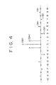
- the coefficient distribution (coefficient profile) of the filter is symmetrical with respect to the centre as shown in Figure 12 of the accompanying drawings and in Table 1 below, even coefficients becoming zero alternately with the exception of the centre coefficient k o .
- the above half-band low pass filter is generally constructed as shown in Figure 13 of the accompanying drawings.
- a read only memory (ROM) 13 o storing therein a centre coefficient k o is connected to a multiplier 12 o which is connected to the point P (centre tap), and multipliers 12 1 , 12 3 ... 12 2n-l are connected to the outputs of odd-numbered delay lines 11 1 , 11 3 ....
- Multipliers 12_ 1 , 12- 3 .... 12 1-2n are connected to the inputs of the odd-numbered delay lines 11 -1 , 11 -3 .... 11 2n-1 sequentially towards the input terminal IN in a manner to be symmetrical to the above with respect to the point P, while the input taps of the even-numbered delay lines 11 2 .... 11 2n - 2 are left unconnected.
- ROMs 13 1 , 13 3 .... 13 2n-1 , 13 -1 , 13 -3 .... 13 1-2n storing coefficients therein are connected to the multipliers 12 1 , 12 3 .... 12 2n - 1 , 12 -1 , 12_ 3 .... 12 1 - 2n , respectively, and the outputs of all of the multipliers 12 are added to one another in an adder 14 and then are delivered to an output terminal OS.
- a digital video signal processing apparatus for curtailing an input signal which is composed of a pair of multiplexed signals of a first video signal component and a second video signal component, the apparatus comprising:
- a digital video signal processing apparatus for curtailing an input signal which is composed of a pair of time-divided signals of a first video signal component and a second video signal component, the apparatus comprising:
- a digital video signal processing apparatus for producing, from a multiplexed signal of a first video signal component and a second video signal component, a pair of component signals of said first and second video signal components, the apparatus comprising:
- the multiplexed or time-divided signals can be curtailed and interpolated in an apparatus of relatively simple construction employing merely a single digital filter. That is, there is provided a digital video signal processing apparatus which is capable of performing proper curtailment and interpolation of multiplexed signals with a relatively simple construction.
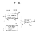
- Figure 1 shows the entire apparatus and Figures 2 and 3 respectively show the basic construction and a specific construction of a half-band high pass filter thereof.
- the apparatus of Figure 1 includes a first in first out (FIFO) memory 20 and a half-band high pass filter 100.
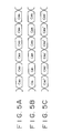
- Multiplexed chrominance signals CB, CR of the 8:4:4 format shown in Figures 5A and 5B are supplied from input terminals 1 and 2, respectively.
- the FIFO memory 20 is supplied as shown with a write/read clock signal and a reset signal and functions as a delay line having a predetermined delay time.
- Outputs of the FIFO memory 20 and of the half-band high pass filter 100 are supplied to an adder 21, an output of which is delivered to an output terminal 3 via a barrel shifter 22.
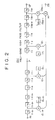
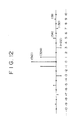
- a basic half-band high pass filter 10H employed in this case is so constructed that, as shown in Figure 2, a tap at a centre point P between an input terminal IN and an output terminal OF is left nonconnected.
- the construction is otherwise exactly the same as in Figure 13.
- the coefficient profile of the half-band high pass filter 10H shown in Figure 2 is such that the centre coefficient k o is zero and the even coefficients also becomes zero alternately as shown in Figure 4.
- the coefficient profile of the half-band high pass filter 10H is symmetrical with respect to the centre point P as shown in Figure 4, where coefficients k 1 , k- 1 .... k 17 , k- 17 of the same value are stored respectively in pairs of ROMS 13 1 , 13_ 1 , .... 13 2n - 1 , 13 1 - 2n to consequently enlarge the circuit scale.
- the basic half-band high pass filter 10H of Figure 2 is so formed that the coefficient profile is turned back at the centre point P, and the coefficients symmetrical with respect to the centre are stored in respective individual ROMs for reducing the circuit scale.
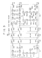
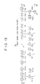
- the half-band high pass filter 100 comprises a unitary circuit (unit) 110 including a single coefficient ROM, and four units 120, 130, 140, 150 having mutually different coefficients and each including two coefficient ROMs.
- a first output terminal 150b of the unit 150 is connected to a first input terminal 140a of the unit 140, and second and third output terminals 140d, 140f of the unit 140 are connected respectively to second and third input terminals 150c, 150e of the unit 150.
- the units 120, 130, 140 are connected in similar manner to that described above such that a first output terminal 120b of the unit 120 is connected to an input terminal 110a of the unit 110, and first and second output terminals 110d, 110f of the unit 110 are connected to second and third input terminals 120c, 120e, respectively, of the unit 120.
- five unitary delay lines 111a to 111e are connected in series between the input terminal 110a and the output terminal 110d.
- An output of the delay line 111 and an output of the delay line 111d are supplied to a multiplier 112 via an adder 115 and a delay line 116, while an input-side tape of the delay line 111d is left non-connected.
- a coefficient ROM 113 is connected to the multiplier 112, an output of which is delivered to the second output terminal 110f via delay lines 117 and 118.
- unit 150 which is structurally the same as any of the units 120, 130 and 140, three unitary delay lines 151a to 151c are connected in series between a first input terminal 150a and the first output terminal 150b, and five unitary delay lines 151d to 151h are connected in series between the second input terminal 150c and a second output terminal 150d.
- a first adder 155a is supplied with the output of the delay line 151c via a delay line 151j and is supplied with the output of the delay line 151e directly.
- a second adder 155b is supplied with the outputs of the delay lines 151b, 151g. Input-side taps of the delay lines 151b, 151e, 151g, 151j are left non-connected.
- the output of the first adder 155a is supplied via a delay line 156a to a first multiplier 152a where it is multiplied by a coefficient obtained from a first ROM 153a.
- the output of the multiplier 152a is supplied via a delay line 157a to a third adder 159a.
- the output of the second adder 155b is supplied via a delay line 156b to a second multiplier 152b where it is multiplied by a coefficient obtained from a second ROM 153b.
- the output of the multiplier 152b is supplied via a delay line 157b to a fourth adder 159b.
- the adders 159a, 159b are connected in series between the third input terminal 150e and a third output terminal 150f together with a delay line 158.
- the delay lines 151 h, 158 connected to the output terminals 150d, 150f serve to attain a timing coincidence of the signals.
- the centre coefficient k o is zero as shown in the coefficient profile of Figure 4.
- the half-band filter 1 OH of Figure 2 (and the half-band filter 100 of Figure 3, equivalent thereto) are regarded as high pass filters each having a reverse characteristic to that of the low pass filter 10L of Figure 13.
- an even sample train and an odd sample train of chrominance signals of the 8:4:4 format are supplied to both the FIFO memory 20 and the half-band high pass filter 100.
- the aliasing component of the odd sample train is extracted from the half-band high pass filter 100 and then is supplied to the adder 21, where such component is added to the even sample train compensated by the FIFO memory 20 with regard to the delay time of the filter 100.
- the chrominance signal obtained from the FIFO memory 20 is a main line signal equivalent to the centre coefficient k o shown in Figure 12.
- the band-limited multiplexed even sample train CBO', CRO', CB2', CR2', .... shown in Figure 5C is delivered from the output terminal 3.
- Figure 6 shows the entire apparatus and Figure 7 shows the basic construction of a digital notch filter thereof.
- component elements corresponding to those in Figure 1 are designated by the same reference signs and a description of these elements is not repeated in full.
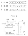
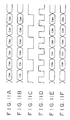
- the apparatus of Figure 6 includes an FIFO memory 20 and a digital notch filter 200, wherein luminance signals of the 8:4:4 format shown in Figures 8A and 8B are supplied from a pair of input terminals 1 and 2, respectively.
- An output of the FIFO memory 20 (functioning as a delay line of a predetermined delay time) and an output of the digital notch filter 200 are supplied to an adder 21, an output of which is delivered to an output terminal 3 via a barrel shifter 22.
- the digital notch filter 200 comprises, as shown in Figure 7, a unit 210 including one coefficient ROM and four units 220, 230, 240, 250 having mutually different coefficients and each including two coefficient ROMs.
- the units 210 to 250 are mutually connected in the same manner as the units 110 to 150 in the high pass filter 100 of Figure 3.
- three unitary delay lines 211a to 211c are connected in series between an input terminal 210a and an output terminal 21 Ob, and both the input and output of the delay line 211 b are supplied to a multiplier 215.
- the construction posterior to the adder 215 is the same as that of the unit 110 in the high pass filter 100 of Figure 3.
- the delay lines 211c, 218 connected to the output terminals 210b, 210f, respectively, serve to attain a timing coincidence of the signals.
- a unitary delay line 251 is connected between a first input terminal 250a and a first output terminal 250b, and three unitary delay lines 251 b to 251d are connected in series between a second input terminal 250c and a second output terminal 250d.
- a first adder 255a is supplied with the output of the delay line 251a via a delay line 251e and is supplied with the output of the delay line 251 b directly.
- a second adder 255b is supplied with the outputs of the delay lines 251 a, 251c.
- the construction posterior to the two adders 255a, 255b is the same as that of the unit 150 in the high pass filter 100 of Figure 3.
- the notch filter 200 used in the second embodiment is formed substantially into an FIR type of filter without any non-connected tap in rows of delay lines, as shown in Figure 7, wherein the coefficients profile thereof is such that all zero points corresponding to the centre and even coefficients in the profile (shown in Figure 4) of the high pass filter 100 is Figure 3 are curtailed.
- the second embodiment of Figure 6 functions as a half-band low pass filter similarly to the first embodiment of Figure 1, but a difference resides in the fact that the coefficients of such half-band low pass filter are divided into a row of odd coefficients and a row of even coefficients, and the filter is composed principally of a FIFO memory (main line) 20 corresponding to the row of odd coefficients and a notch filter 200 corresponding to the row of even coefficients and having an amplitude characteristic which is skew symmetrical with respect to a frequency fs/4.
- the composite amplitude characteristic (absolute value) of the filter 200 is such that a zero level (notch) is at the frequency fs/4, and the phase is inverted at the notch as a turnover point.
- an even sample train and an odd sample train of the luminance signal based on the 8:4:4 format are time-divided into two channels and are supplied to the FIFO memory 20 and the notch filter 200, respectively.
- a band-limited even sample train YO', Y2' .... shown in Figure 9C is delivered from the output terminal 3.
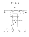
- Figure 9 shows the entire apparatus and Figure 10 shows the basic construction of a demultiplexer thereof.
- component elements corresponding to those in Figures 1 and 6 are designated by the same reference signs and a description of these elements is not repeated in full.
- multiplexed chrominance signals CB, CR of the 4:2:2 format shown in Figure 11A are supplied from an input terminal 4 to both an FIFO memory 20 and a half-band high pass filter 100.
- An output of the FIFO memory 20 (functioning as a delay line of a predetermined delay time) and an output of the half-band high pass filter 100 are supplied to input terminals 30a, 30b, respectively, of a demultiplexer 30, output terminals 30c, 30d of which are connected to output terminals 5, 6, respectively, of the apparatus.
- the demultiplexer 30 includes four multipliers (switches) 31, 32, 33, 34.
- One input terminal 30a of the demultiplexer 30 is connected directly to the first and third switches 31, 33, while another input terminal 30b thereof is connected via a unitary delay line 35 to the second and fourth switches 32, 34.
- Switching pulses shown in Figure 11C from a control terminal 30s are supplied to the switches 31, 34 directly and are supplied to the switches 32, 33 via an inverting amplifier 36.
- Outputs of the first and second switches 31, 32 are delivered to one output terminal 30c via an adder 37 and a unitary delay line 39, and outputs of the third and fourth switches 33, 34 are delivered to another output terminal 30c via another adder 38.
- an even sample train of chrominance signals of the 4:2:2 format, where CB, CR are multiplexed per sample as shown in Figure 11A is supplied to the FIFO memory 20 and the half-band high pass filter 100, so that an even sample train similar to the original data is outputted from the FIFO memory 20, while interpolated data of the even sample train, i.e., the odd sample train shown in Figure 11 B, is outputted from the high pass filter 100.
- the outputs of the FIFO memory 20 and the high pass filter 100 can be distributed respectively to two channels of the 8:4:4 format.
- the first and fourth switches 31, 34 and the second and third switches 32, 33 are turned on and off alternately by the switching pulses shown in Figure 11 C, which are formed on the basis of a system clock signal shown in Figure 11 D.
- An even sample train of the chrominance signals shown in Figure 11A is distributed alternately to the adders 37, 38 by the first and second switches 31, 32, while an odd sample train of the chrominance signals shown in Figure 11 B is distributed alternately to the adders 37 and 38 by the third and fourth switches 33, 34 after being delayed for a time equal to one sample by the delay line 35.
- the original data and the interpolated data are combined with each other and are processed as chrominance signals of the 8:4:4 format, whereby the multiplexed chrominance signals can be interpolated and oversampled in a relatively simple construction employing a signal digital filter.
- a digital video signal processing apparatus for curtailing and interpolating digital video signals of a component format comprises a half-band high pass filter having a coefficient profile equivalent to that obtained by setting the centre coefficient of a half-band low pass filter to zero, or a notch filter having a coefficient profile equivalent to that obtained by curtailing the centre and even coefficients of a half-band low pass filter, and a delay line having a predetermined delay time, and achieves the improvement of being capable of performing curtailment and interpolation of multiplexed signals with a relatively simple construction employing a single digital filter.
Landscapes
- Engineering & Computer Science (AREA)
- Multimedia (AREA)
- Signal Processing (AREA)
- Physics & Mathematics (AREA)
- Computer Hardware Design (AREA)
- Mathematical Physics (AREA)
- Television Systems (AREA)
- Compression Or Coding Systems Of Tv Signals (AREA)
- Picture Signal Circuits (AREA)
- Television Signal Processing For Recording (AREA)
- Processing Of Color Television Signals (AREA)
Applications Claiming Priority (2)
| Application Number | Priority Date | Filing Date | Title |
|---|---|---|---|
| JP33834990A JP2953052B2 (ja) | 1990-11-30 | 1990-11-30 | デジタル映像信号処理装置 |
| JP338349/90 | 1990-11-30 |
Publications (3)
| Publication Number | Publication Date |
|---|---|
| EP0488680A2 true EP0488680A2 (de) | 1992-06-03 |
| EP0488680A3 EP0488680A3 (en) | 1993-05-12 |
| EP0488680B1 EP0488680B1 (de) | 1997-04-23 |
Family
ID=18317314
Family Applications (1)
| Application Number | Title | Priority Date | Filing Date |
|---|---|---|---|
| EP19910310934 Expired - Lifetime EP0488680B1 (de) | 1990-11-30 | 1991-11-27 | Vorrichtung zum Verarbeiten eines digitalen Videosignals |
Country Status (5)
| Country | Link |
|---|---|
| US (2) | US5194939A (de) |
| EP (1) | EP0488680B1 (de) |
| JP (1) | JP2953052B2 (de) |
| KR (1) | KR100254501B1 (de) |
| DE (1) | DE69125800T2 (de) |
Families Citing this family (8)
| Publication number | Priority date | Publication date | Assignee | Title |
|---|---|---|---|---|
| JP2953052B2 (ja) * | 1990-11-30 | 1999-09-27 | ソニー株式会社 | デジタル映像信号処理装置 |
| JP3179267B2 (ja) * | 1993-01-19 | 2001-06-25 | 三菱電機株式会社 | フィルタ及びこのフィルタを用いたキャリア位相推定装置 |
| JPH07327130A (ja) * | 1994-06-01 | 1995-12-12 | Fuji Photo Film Co Ltd | 画像読取装置 |
| KR0168998B1 (ko) * | 1995-10-26 | 1999-03-20 | 김광호 | 점순차 색차신호 변환용 다위상필터 |
| FI972346A7 (fi) * | 1997-06-02 | 1998-12-03 | Nokia Corp | Menetelmä ja laitteisto siirtoyhteyden toteuttamiseksi |
| US6616254B1 (en) * | 1997-06-20 | 2003-09-09 | Itran Communications Ltd. | Code shift keying transmitter for use in a spread spectrum communications system |
| JP2003224456A (ja) * | 2002-01-31 | 2003-08-08 | Leader Electronics Corp | 時分割多重信号をフィルタ処理するためのデジタル・フィルタ |
| US8233529B2 (en) * | 2008-08-14 | 2012-07-31 | Mediatek Inc. | Video decoder |
Family Cites Families (11)
| Publication number | Priority date | Publication date | Assignee | Title |
|---|---|---|---|---|
| JPS57208722A (en) * | 1981-06-18 | 1982-12-21 | Sony Corp | Digital filter |
| US4538178A (en) * | 1983-06-24 | 1985-08-27 | Rca Corporation | Digital signal peaking apparatus with controllable peaking level |
| JPS6093682A (ja) * | 1983-10-25 | 1985-05-25 | Sony Corp | デイジタル非線形プリエンフアシス回路 |
| GB2153618B (en) * | 1984-02-01 | 1987-07-22 | British Broadcasting Corp | Processing of periodic signals |
| US4727506A (en) * | 1985-03-25 | 1988-02-23 | Rca Corporation | Digital scaling circuitry with truncation offset compensation |
| DE3539415A1 (de) * | 1985-11-07 | 1987-05-14 | Bosch Gmbh Robert | Verfahren und schaltungsanordnung zum erkennen und verdecken von fehlern in einem digitalen videosignal |
| JPS631276A (ja) * | 1986-06-20 | 1988-01-06 | Olympus Optical Co Ltd | カラ−撮像装置 |
| US4835723A (en) * | 1987-04-03 | 1989-05-30 | Tektronix, Inc. | Phase coordinated multistage digital filter |
| IT1227520B (it) * | 1988-12-06 | 1991-04-12 | Sgs Thomson Microelectronics | Filtro digitale programmabile |
| US4947408A (en) * | 1989-05-12 | 1990-08-07 | The United States Of America As Represented By The Administrator Of The National Aeronautics And Space Administration | Digital carrier demodulator employing components working beyond normal limits |
| JP2953052B2 (ja) * | 1990-11-30 | 1999-09-27 | ソニー株式会社 | デジタル映像信号処理装置 |
-
1990
- 1990-11-30 JP JP33834990A patent/JP2953052B2/ja not_active Expired - Lifetime
-
1991
- 1991-11-22 US US07/796,378 patent/US5194939A/en not_active Expired - Lifetime
- 1991-11-27 EP EP19910310934 patent/EP0488680B1/de not_active Expired - Lifetime
- 1991-11-27 DE DE69125800T patent/DE69125800T2/de not_active Expired - Fee Related
- 1991-11-30 KR KR1019910021989A patent/KR100254501B1/ko not_active Expired - Fee Related
-
1993
- 1993-02-23 US US08/021,521 patent/US5307157A/en not_active Expired - Lifetime
Also Published As
| Publication number | Publication date |
|---|---|
| DE69125800T2 (de) | 1997-09-04 |
| EP0488680B1 (de) | 1997-04-23 |
| KR100254501B1 (ko) | 2000-05-01 |
| US5194939A (en) | 1993-03-16 |
| JP2953052B2 (ja) | 1999-09-27 |
| DE69125800D1 (de) | 1997-05-28 |
| US5307157A (en) | 1994-04-26 |
| JPH04207776A (ja) | 1992-07-29 |
| KR920011254A (ko) | 1992-06-27 |
| EP0488680A3 (en) | 1993-05-12 |
Similar Documents
| Publication | Publication Date | Title |
|---|---|---|
| US4712130A (en) | Chrominance signal frequency converter as for a pix-in-pix television receiver | |
| EP0423921B1 (de) | Vorrichtung und Verfahren zur Verwandlung digitaler Videosignale | |
| EP0048569B1 (de) | Fehlerverbergung in digitalen Fernsehsignalen | |
| EP0591970A2 (de) | Abtastraten Umwandlungssystem durch Annäherung | |
| US4903019A (en) | Sampling frequency converter for converting a lower sampling frequency to a higher sampling frequency and a method therefor | |
| US4750039A (en) | Circuitry for processing a field of video information to develop two compressed fields | |
| EP0488680B1 (de) | Vorrichtung zum Verarbeiten eines digitalen Videosignals | |
| US5166792A (en) | Video signal processing and video stores | |
| JP2513661B2 (ja) | 時間軸圧縮多重伝送用コ−デック | |
| EP0382245B1 (de) | Gerät zur Umformung von Farbsignalkomponenten | |
| US5394276A (en) | Method and apparatus for two-channel recording of video signals | |
| US5249038A (en) | System and method for converting component video signals to a composite video signal compatible with the pal standard | |
| JPS59205889A (ja) | フイルタ | |
| US5929905A (en) | Imaging apparatus | |
| US4707737A (en) | Band compression apparatus for a video signal | |
| US5119176A (en) | System and method for direct digital conversion of digital component video signals to NTSC signal | |
| US5200812A (en) | Sampling frequency down-converting apparatus | |
| US4907072A (en) | Mosaic picture generation circuit | |
| JP3782510B2 (ja) | 画像処理装置 | |
| JP2903580B2 (ja) | デジタル映像信号の多チャンネル記録再生装置 | |
| JP2587159B2 (ja) | 色信号補間回路 | |
| JPH08102870A (ja) | トランスバーサルフィルタ制御回路と、ゴースト除去及びアスペクト変換装置 | |
| JPH01245783A (ja) | 線順次色信号の配列補正回路 | |
| HK16196A (en) | Horizontal filter for a luminance signal and a chrominance signal |
Legal Events
| Date | Code | Title | Description |
|---|---|---|---|
| PUAI | Public reference made under article 153(3) epc to a published international application that has entered the european phase |
Free format text: ORIGINAL CODE: 0009012 |
|
| AK | Designated contracting states |
Kind code of ref document: A2 Designated state(s): DE FR GB |
|
| PUAL | Search report despatched |
Free format text: ORIGINAL CODE: 0009013 |
|
| PUAF | Information related to the publication of a search report (a3 document) modified or deleted |
Free format text: ORIGINAL CODE: 0009199SEPU |
|
| AK | Designated contracting states |
Kind code of ref document: A3 Designated state(s): DE FR GB |
|
| D17D | Deferred search report published (deleted) | ||
| PUAL | Search report despatched |
Free format text: ORIGINAL CODE: 0009013 |
|
| AK | Designated contracting states |
Kind code of ref document: A3 Designated state(s): DE FR GB |
|
| 17P | Request for examination filed |
Effective date: 19931001 |
|
| 17Q | First examination report despatched |
Effective date: 19950816 |
|
| GRAG | Despatch of communication of intention to grant |
Free format text: ORIGINAL CODE: EPIDOS AGRA |
|
| GRAH | Despatch of communication of intention to grant a patent |
Free format text: ORIGINAL CODE: EPIDOS IGRA |
|
| GRAH | Despatch of communication of intention to grant a patent |
Free format text: ORIGINAL CODE: EPIDOS IGRA |
|
| GRAA | (expected) grant |
Free format text: ORIGINAL CODE: 0009210 |
|
| AK | Designated contracting states |
Kind code of ref document: B1 Designated state(s): DE FR GB |
|
| REF | Corresponds to: |
Ref document number: 69125800 Country of ref document: DE Date of ref document: 19970528 |
|
| ET | Fr: translation filed | ||
| PLBE | No opposition filed within time limit |
Free format text: ORIGINAL CODE: 0009261 |
|
| STAA | Information on the status of an ep patent application or granted ep patent |
Free format text: STATUS: NO OPPOSITION FILED WITHIN TIME LIMIT |
|
| 26N | No opposition filed | ||
| REG | Reference to a national code |
Ref country code: GB Ref legal event code: IF02 |
|
| PGFP | Annual fee paid to national office [announced via postgrant information from national office to epo] |
Ref country code: FR Payment date: 20031110 Year of fee payment: 13 |
|
| PGFP | Annual fee paid to national office [announced via postgrant information from national office to epo] |
Ref country code: GB Payment date: 20031126 Year of fee payment: 13 |
|
| PGFP | Annual fee paid to national office [announced via postgrant information from national office to epo] |
Ref country code: DE Payment date: 20031204 Year of fee payment: 13 |
|
| PG25 | Lapsed in a contracting state [announced via postgrant information from national office to epo] |
Ref country code: GB Free format text: LAPSE BECAUSE OF NON-PAYMENT OF DUE FEES Effective date: 20041127 |
|
| PG25 | Lapsed in a contracting state [announced via postgrant information from national office to epo] |
Ref country code: DE Free format text: LAPSE BECAUSE OF NON-PAYMENT OF DUE FEES Effective date: 20050601 |
|
| GBPC | Gb: european patent ceased through non-payment of renewal fee |
Effective date: 20041127 |
|
| PG25 | Lapsed in a contracting state [announced via postgrant information from national office to epo] |
Ref country code: FR Free format text: LAPSE BECAUSE OF NON-PAYMENT OF DUE FEES Effective date: 20050729 |
|
| REG | Reference to a national code |
Ref country code: FR Ref legal event code: ST |