EP0487216B1 - Input buffer with noise filter - Google Patents
Input buffer with noise filter Download PDFInfo
- Publication number
- EP0487216B1 EP0487216B1 EP91310017A EP91310017A EP0487216B1 EP 0487216 B1 EP0487216 B1 EP 0487216B1 EP 91310017 A EP91310017 A EP 91310017A EP 91310017 A EP91310017 A EP 91310017A EP 0487216 B1 EP0487216 B1 EP 0487216B1
- Authority
- EP
- European Patent Office
- Prior art keywords
- input
- schmitt trigger
- input buffer
- voltage level
- coupled
- Prior art date
- Legal status (The legal status is an assumption and is not a legal conclusion. Google has not performed a legal analysis and makes no representation as to the accuracy of the status listed.)
- Expired - Lifetime
Links
Images
Classifications
-
- H—ELECTRICITY
- H03—ELECTRONIC CIRCUITRY
- H03K—PULSE TECHNIQUE
- H03K3/00—Circuits for generating electric pulses; Monostable, bistable or multistable circuits
- H03K3/02—Generators characterised by the type of circuit or by the means used for producing pulses
- H03K3/027—Generators characterised by the type of circuit or by the means used for producing pulses by the use of logic circuits, with internal or external positive feedback
- H03K3/037—Bistable circuits
- H03K3/0377—Bistables with hysteresis, e.g. Schmitt trigger
Definitions
- the present invention relates generally to an input buffer for use in an integrated circuit.
- the present invention more particularly relates to such an input buffer which buffers input digital signals and filters noise.
- Integrated circuits are well known in the art. Some integrated circuits are intended for use in digital processing systems in association with other devices external to the digital processing integrated circuit. In many instances, the devices external to the digital integrated circuits generate spurious or noise signals, which, if not filtered, would provide false inputs to the digital integrated circuit.
- input buffering is preferable in digital integrated circuits. Such input buffering assures that valid logic one or logic zero inputs are properly interpreted and filter spurious signals or noise which are generally either shorter in duration than valid logic levels or of lesser magnitude than valid logic levels.
- Input buffers have taken different forms.
- One known input buffer includes a chain of buffering inverters coupled to one or more AND gates.
- the inverters buffer the input signals to appropriate signal levels and the AND gates differentiate the valid input transitions from noise.
- Unfortunately, such input buffers impose gate delays and reduce the operating speed of the integrated circuits in which they are employed.
- such input buffers require many active devices which occupy considerable integrated circuit surface area to achieve a filtering function.
- EP-A-0 107 189 describes a Schmitt trigger circuit which may be used as an input buffer.
- Figure 11 of that application shows a Schmitt trigger circuit having an input for receiving digital input signals; an output; an inverter coupled to the output and first and second transmission gates each coupled between the input and the inverter.
- the transmission gates and the inverter form a selection circuit which provides the output with a first voltage level if the input signal is below a threshold voltage and a second voltage level if the input signal is above the threshold voltage.
- the present invention relates to such an improved input buffer which both buffers digital input signals and which filters noise without requiring a large number of active devices on the integrated circuit on which it is employed.
- an input buffer for buffering digital input signals having first and second voltage levels and for filtering noise signals
- said input buffer comprising: an input adapted to receive said digital input signals; an output; threshold circuit means coupled to said output and having an input, said threshold circuit means being arranged for providing said output with said first voltage level responsive to an input signal being below a threshold voltage and being arranged for providing said output with said second voltage level responsive to an input signal being above said threshold voltage, said threshold voltage being closer in potential to one of said voltage levels than the other said voltage level; first transfer means coupled between said input buffer input and said threshold circuit means input for conveying, when selectively enabled by output of said threshold circuit means, to said threshold circuit means, input signals which are in transition from said one voltage level to said other voltage level, said first transfer means being arranged to have a relatively slow response; and second transfer means coupled between said input buffer input and said threshold circuit means input for conveying, when selectively enabled by output of said threshold circuit means, to said threshold circuit means, input signals which are in transition from said other voltage level to said one
- the input buffer includes an input adapted to receive the digital input signals, an output, and threshold circuit means coupled to the output and having an input.
- the threshold circuit means is arranged for providing the output with the first voltage level responsive to an input signal being below a threshold voltage and is arranged for providing the output with a second voltage level responsive to an input signal being above the threshold voltage.
- the threshold voltage is closer in potential to one of the voltage levels than the other voltage level.
- the input buffer further includes first transfer means coupled between the input buffer input and the threshold circuit means input for conveying, to the threshold circuit means, input signals which are in transition from the one voltage level to the other voltage level.
- the first transfer means is arranged to have a slow response to transitions from the one voltage level to the other voltage level.
- the input buffer further includes second transfer means coupled between the input buffer input and the threshold circuit means input for conveying, to the threshold circuit means, input signals which are in transition from the other voltage level to the one voltage level.
- the second transfer means is arranged to have a fast response to transitions from the other voltage level to the one voltage level.
- the input buffer includes an input adapted to receive the digital input signals, wherein the digital input signals have rising and falling edges, an output, and a Schmitt trigger coupled to the output for providing the buffered digital signals.
- the Schmitt trigger has an input and is arranged to provide a fast response to digital signal rising edges and a slow response to digital signal falling edges.
- the input buffer further includes first transfer means coupled between the input buffer input and the Schmitt trigger input to convey the rising edges of the input digital signals to the Schmitt trigger and is arranged to have a slow response to the input digital signal rising edges.
- the input buffer further includes second transfer means coupled between the input buffer input and the Schmitt trigger input to convey the falling edges of the input digital signals to the Schmitt trigger and is arranged to have a fast response to the digital signal falling edges.
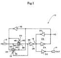
- the input buffer 10 generally includes an input 12, an output 14, a threshold circuit means 16, a first transfer means or gate 18, and a second transfer means or gate 20.
- the input buffer 10 is arranged to receive at its input 12 digital input signals which, during steady state conditions, have a first voltage level of, for example, zero volts, and a second voltage level of, for example, five volts.
- the threshold circuit 16 provides at the output 14 of the input buffer 10 corresponding first and second voltage levels in response to the voltage levels at input 12.
- the threshold circuit 16 includes a Schmitt trigger 22 which includes a first inverter 24, a second inverter 26, and a third inverter 28.
- the first and second inverters 24 and 26 are reversed coupled and the third inverter is coupled in series with the reversed coupled inverters 24 and 26 as illustrated.
- a fourth inverter 30 of the threshold circuit 16 couples the Schmitt trigger 22 to the output 14 of the input buffer 10.
- the Schmitt trigger 22 establishes a threshold voltage at the input 32 of inverter 28 of approximately 1.5 volts. As will be seen hereinafter, when the voltage at the input 32 of inverter 28 is below the threshold voltage, the input buffer will provide at output 14 the first voltage level of zero volts and when the voltage at input 32 of inverter 28 is above the threshold voltage, the input buffer 10 will provide at output 14 the second voltage level of five volts.
- the Schmitt trigger is arranged to have a fast response to the rising edges of digital input signals received at input 32 of inverter 28 and a comparatively slow response to the falling edges of the digital input signals received at the input 32 of inverter 28.
- the first and second transfer gates 18 and 20 are coupled between the input 12 of the input buffer 10 and the input 32 of inverter 28.
- the first transfer gate 18 is formed by a first field-effect transistor 34 which is coupled in parallel with a second field-effect transistor 36.
- the first field-effect transistor 34 is an N-Channel field-effect transistor and the second field-effect transistor 36 is a P-Channel field-effect transistor.
- the sources of the field-effect transistors 34 and 36 are coupled together and to the input 12 of the input buffer 10.
- the drains of the field-effect transistors 34 and 36 are also coupled together and to the input 32 of inverter 28.
- the second transfer gate 20 is formed by a first field-effect transistor 38 coupled in parallel with a second field-effect transistor 40.
- the first field-effect transistor 38 is an N-Channel field-effect transistor and the second field-effect transistor 40 is a P-Channel field-effect transistor.
- the sources of the field-effect transistors 38 and 40 are coupled together and to the input 12 of the input buffer 10.
- the drains of the field-effect transistors 38 and 40 are also coupled together and to the input 32 of inverter 28.
- the first transfer gate 18 transfers the rising edges of the digital input signals received at input 12 to the Schmitt trigger 22 and the second transfer gate 20 conveys the falling edges of the digital input signals received at input 12 to the Schmitt trigger 22 at the input 32 of inverter 28.
- the first and second transfer gates 18 and 20 are enabled by the Schmitt trigger 22.
- the common junction 40 of inverters 24 and 26 of the Schmitt trigger 22 is coupled directly to the gate 42 of field-effect transistor 36 and the gate 44 of the field-effect transistor 38.
- the common junction 40 is also coupled through an inverter 46 to the gate 48 of field-effect transistor 40 and to the gate 50 of field-effect transistor 34.
- the gate 42 of field-effect transistor 36 forms a first enable input of the first transfer gate 18 and the gate 48 of field-effect transistor 40 forms a second enable input of the second transfer gate 20.
- the first and second transfer gates 18 and 20 are enabled in response to receiving at the first and second enable inputs 42 and 48 respectively a low and a high logic level from the Schmitt trigger 22.
- the Schmitt trigger 22 will provide a low logic level to the first enable input 42 to enable the first transfer gate 18 to convey the next rising edge of the input signal at input 12 to the input 32 of inverter 28.
- the Schmitt trigger 22 will provide through inverter 46 a low logic level to the enable input 48 to enable the second transfer gate to convey the next falling edge of the input signal at input 12 to the input 32 of inverter 28.
- the first transfer gate 18 is arranged to have a slow response to the rising edges received at the input 12. Such a slow response may be obtained, as well known in the art, by configuring the channels of the field-effect transistors 34 and 36 to impose a high resistance and high capacitance to the input signals received at the sources of the field-effect transistors 34 and 36.
- the second transfer gate 20 is arranged to have a fast response to the falling edges of the input signals received at the input 12 of the input buffer 10.
- a fast response may be obtained, in a manner well known in the art, by configuring the channels of the field-effect transistors 38 and 40 to impose a relatively small resistance and capacitance to the falling edges of the input signals received at the sources of the field-effect transistors 38 and 40.
- the slow response of the first transfer gate 18 is provided because the Schmitt trigger 22 has a relatively fast response to rising edges received at the input 32 of inverter 28 resulting from the threshold voltage being closer to the first voltage level of zero volts than the second voltage level of five volts.
- the fast response of the second transfer gate 20 is provided because the Schmitt trigger 22 has a relatively slow response to falling edges received at the input 32 of inverter 28 due to the threshold voltage being further in potential from the second voltage level of five volts than the first voltage level of zero volts.
- the first and second transfer gates have asymmetrical characteristics with respect to the input signals received at input 12 to compensate for the asymmetrical characteristics of the Schmitt trigger 22.
- the asymmetrical characteristics of the first and second transfer gates 18 and 20 enable the Schmitt trigger 22 to discriminate noise from valid input signal transitions without imposing excessive gate delays characteristic of prior art input buffers.
- the input buffer 10 embodying the present invention is capable of operating at higher speeds than prior art input buffers while still providing the important function of noise filtering.
- the output 14 will also provide a low logic level.
- the common junction 40 of the Schmitt trigger 22 will also be at a low logic level which is impressed upon the enable input 42 of the first transfer gate 18 to enable the first transfer gate 18 to convey the next rising edge of the digital input at input 12.
- the output 14 When the input 12 is at a high logic level, the output 14 will also be at a high logic level.
- the common junction 40 will be at a high logic level which is inverted by the inverter 46 so that the second enable input 48 will receive a low logic level to enable the second transfer gate 20 to convey the next falling edge of the digital input signal at input 12.
- the input signal at input 12 rises from a low logic level, it is conveyed through the first transfer gate 18 to the Schmitt trigger 22 at input 32 of inverter 28. Because the first transfer gate 18 has a slow response to input rising edges, the first transfer gate 18 slows down the transition seen at the input 32 of inverter 28. If the rise in the input voltage is due to noise, it will fall back to zero before the input voltage exceeds the threshold of the Schmitt trigger 22. However, if the rising edge at input 12 is a valid transition, the rising voltage at input 12 will continue to rise above the threshold voltage at input 32 of inverter 28 of the Schmitt trigger 22 to cause the Schmitt trigger to change state to cause the voltage at output 14 to go from a low logic level to a high logic level.
- the delay in the first transfer gate 18 compensates for the fast response of the Schmitt trigger to rising edges at the input 32 of inverter 28.
- the falling edge When the signal on input 12 falls from the high logic level, the falling edge propagates through the second transfer gate 20 to the Schmitt trigger. Because the second transfer gate 20 has a fast response to input falling edges, the falling edge will be propagated to the Schmitt trigger 22 at input 32 of inverter 28 without any delay. Since the threshold voltage of the Schmitt trigger is further from the high voltage level than the low voltage level, it will respond slowly to a falling input signal. Hence, if the falling input signal is due to noise, it will return to the high voltage level without going below the threshold voltage of the Schmitt trigger 22.
- the input signal will continue to fall to below the threshold voltage of the Schmitt trigger 22 at input 32 of inverter 28 to cause the Schmitt trigger 22 to change state to provide a transition at output 14 from the high voltage level to the low voltage level.
- This causes the second transfer gate 20 to then be disabled and the first transfer gate 18 to once again be enabled for conveying the next rising edge of the input signal at input 12.
- the present invention provides a new and improved input buffer with noise filtering. Because the first transfer gate has a slow response, rising transitions due to noise may be filtered even though the Schmitt trigger has a fast response to rising edges. Conversely, the second transfer gate 20 has a fast response due to the relatively slow response of the Schmitt trigger 22 to falling edges. As a result, falling input signals due to noise may also be filtered allowing only valid falling edge transitions to effect the output of the buffer. As a result, noise filtering is achieved within the input buffer without resulting to inverter chains and AND gates which in the past have imposed gate delays. Also, as a result, the input buffer of the present invention is capable of filtering noise while responding to valid transitions in the digital input signal without adversely affecting operating speed.
Abstract
Description
- The present invention relates generally to an input buffer for use in an integrated circuit. The present invention more particularly relates to such an input buffer which buffers input digital signals and filters noise.
- Integrated circuits are well known in the art. Some integrated circuits are intended for use in digital processing systems in association with other devices external to the digital processing integrated circuit. In many instances, the devices external to the digital integrated circuits generate spurious or noise signals, which, if not filtered, would provide false inputs to the digital integrated circuit.
- As a result, input buffering is preferable in digital integrated circuits. Such input buffering assures that valid logic one or logic zero inputs are properly interpreted and filter spurious signals or noise which are generally either shorter in duration than valid logic levels or of lesser magnitude than valid logic levels.
- Input buffers have taken different forms. One known input buffer includes a chain of buffering inverters coupled to one or more AND gates. The inverters buffer the input signals to appropriate signal levels and the AND gates differentiate the valid input transitions from noise. Unfortunately, such input buffers impose gate delays and reduce the operating speed of the integrated circuits in which they are employed. In addition, such input buffers require many active devices which occupy considerable integrated circuit surface area to achieve a filtering function.
- EP-A-0 107 189 describes a Schmitt trigger circuit which may be used as an input buffer. Figure 11 of that application shows a Schmitt trigger circuit having an input for receiving digital input signals; an output; an inverter coupled to the output and first and second transmission gates each coupled between the input and the inverter. The transmission gates and the inverter form a selection circuit which provides the output with a first voltage level if the input signal is below a threshold voltage and a second voltage level if the input signal is above the threshold voltage.
- There is therefore a need in the art for a new and improved input buffer which provides both input buffering and noise filtering. The present invention relates to such an improved input buffer which both buffers digital input signals and which filters noise without requiring a large number of active devices on the integrated circuit on which it is employed.
- According to the present invention, there is provided an input buffer for buffering digital input signals having first and second voltage levels and for filtering noise signals, said input buffer comprising: an input adapted to receive said digital input signals; an output; threshold circuit means coupled to said output and having an input, said threshold circuit means being arranged for providing said output with said first voltage level responsive to an input signal being below a threshold voltage and being arranged for providing said output with said second voltage level responsive to an input signal being above said threshold voltage, said threshold voltage being closer in potential to one of said voltage levels than the other said voltage level; first transfer means coupled between said input buffer input and said threshold circuit means input for conveying, when selectively enabled by output of said threshold circuit means, to said threshold circuit means, input signals which are in transition from said one voltage level to said other voltage level, said first transfer means being arranged to have a relatively slow response; and second transfer means coupled between said input buffer input and said threshold circuit means input for conveying, when selectively enabled by output of said threshold circuit means, to said threshold circuit means, input signals which are in transition from said other voltage level to said one voltage level, said second transfer means having a relatively fast response.
- We describe an input buffer for buffering digital input signals having first and second voltage levels and filtering noise signals of short duration. The input buffer includes an input adapted to receive the digital input signals, an output, and threshold circuit means coupled to the output and having an input. The threshold circuit means is arranged for providing the output with the first voltage level responsive to an input signal being below a threshold voltage and is arranged for providing the output with a second voltage level responsive to an input signal being above the threshold voltage. The threshold voltage is closer in potential to one of the voltage levels than the other voltage level. The input buffer further includes first transfer means coupled between the input buffer input and the threshold circuit means input for conveying, to the threshold circuit means, input signals which are in transition from the one voltage level to the other voltage level. The first transfer means is arranged to have a slow response to transitions from the one voltage level to the other voltage level. The input buffer further includes second transfer means coupled between the input buffer input and the threshold circuit means input for conveying, to the threshold circuit means, input signals which are in transition from the other voltage level to the one voltage level. The second transfer means is arranged to have a fast response to transitions from the other voltage level to the one voltage level.
- We further describe an input buffer for providing buffered digital signals in response to input signals and for filtering noise. The input buffer includes an input adapted to receive the digital input signals, wherein the digital input signals have rising and falling edges, an output, and a Schmitt trigger coupled to the output for providing the buffered digital signals. The Schmitt trigger has an input and is arranged to provide a fast response to digital signal rising edges and a slow response to digital signal falling edges. The input buffer further includes first transfer means coupled between the input buffer input and the Schmitt trigger input to convey the rising edges of the input digital signals to the Schmitt trigger and is arranged to have a slow response to the input digital signal rising edges. The input buffer further includes second transfer means coupled between the input buffer input and the Schmitt trigger input to convey the falling edges of the input digital signals to the Schmitt trigger and is arranged to have a fast response to the digital signal falling edges.
- An-example of the invention is illustrated in the accompanying drawing wherein the sole figure is a schematic circuit diagram of an input buffer.
- Referring to this sole Figure, the
input buffer 10 generally includes aninput 12, anoutput 14, a threshold circuit means 16, a first transfer means orgate 18, and a second transfer means orgate 20. Theinput buffer 10 is arranged to receive at itsinput 12 digital input signals which, during steady state conditions, have a first voltage level of, for example, zero volts, and a second voltage level of, for example, five volts. Thethreshold circuit 16 provides at theoutput 14 of theinput buffer 10 corresponding first and second voltage levels in response to the voltage levels atinput 12. - The
threshold circuit 16 includes a Schmitttrigger 22 which includes afirst inverter 24, asecond inverter 26, and athird inverter 28. The first andsecond inverters inverters fourth inverter 30 of thethreshold circuit 16 couples the Schmitt trigger 22 to theoutput 14 of theinput buffer 10. - The Schmitt
trigger 22 establishes a threshold voltage at theinput 32 ofinverter 28 of approximately 1.5 volts. As will be seen hereinafter, when the voltage at theinput 32 ofinverter 28 is below the threshold voltage, the input buffer will provide atoutput 14 the first voltage level of zero volts and when the voltage atinput 32 ofinverter 28 is above the threshold voltage, theinput buffer 10 will provide atoutput 14 the second voltage level of five volts. Because the threshold voltage of the Schmitt trigger is closer to the first voltage level of zero volts than the second voltage level of five volts, the Schmitt trigger is arranged to have a fast response to the rising edges of digital input signals received atinput 32 ofinverter 28 and a comparatively slow response to the falling edges of the digital input signals received at theinput 32 ofinverter 28. - The first and
second transfer gates input 12 of theinput buffer 10 and theinput 32 ofinverter 28. Thefirst transfer gate 18 is formed by a first field-effect transistor 34 which is coupled in parallel with a second field-effect transistor 36. The first field-effect transistor 34 is an N-Channel field-effect transistor and the second field-effect transistor 36 is a P-Channel field-effect transistor. The sources of the field-effect transistors input 12 of theinput buffer 10. The drains of the field-effect transistors input 32 ofinverter 28. - Similarly, the
second transfer gate 20 is formed by a first field-effect transistor 38 coupled in parallel with a second field-effect transistor 40. The first field-effect transistor 38 is an N-Channel field-effect transistor and the second field-effect transistor 40 is a P-Channel field-effect transistor. The sources of the field-effect transistors input 12 of theinput buffer 10. the drains of the field-effect transistors input 32 ofinverter 28. - As will be seen hereinafter, the
first transfer gate 18 transfers the rising edges of the digital input signals received atinput 12 to the Schmitttrigger 22 and thesecond transfer gate 20 conveys the falling edges of the digital input signals received atinput 12 to the Schmitt trigger 22 at theinput 32 ofinverter 28. To enable thetransfer gates second transfer gates common junction 40 ofinverters trigger 22 is coupled directly to thegate 42 of field-effect transistor 36 and thegate 44 of the field-effect transistor 38. Thecommon junction 40 is also coupled through aninverter 46 to thegate 48 of field-effect transistor 40 and to thegate 50 of field-effect transistor 34. Thegate 42 of field-effect transistor 36 forms a first enable input of thefirst transfer gate 18 and thegate 48 of field-effect transistor 40 forms a second enable input of thesecond transfer gate 20. - The first and
second transfer gates inputs output 14 is at a low logic level, the Schmitttrigger 22 will provide a low logic level to the first enableinput 42 to enable thefirst transfer gate 18 to convey the next rising edge of the input signal atinput 12 to theinput 32 ofinverter 28. When theoutput 14 is at the high logic level, the Schmitttrigger 22 will provide through inverter 46 a low logic level to the enableinput 48 to enable the second transfer gate to convey the next falling edge of the input signal atinput 12 to theinput 32 ofinverter 28. - In accordance with the present invention, the
first transfer gate 18 is arranged to have a slow response to the rising edges received at theinput 12. Such a slow response may be obtained, as well known in the art, by configuring the channels of the field-effect transistors effect transistors - Also in accordance with the present invention, the
second transfer gate 20 is arranged to have a fast response to the falling edges of the input signals received at theinput 12 of theinput buffer 10. Such a fast response may be obtained, in a manner well known in the art, by configuring the channels of the field-effect transistors effect transistors - The slow response of the
first transfer gate 18 is provided because the Schmitttrigger 22 has a relatively fast response to rising edges received at theinput 32 ofinverter 28 resulting from the threshold voltage being closer to the first voltage level of zero volts than the second voltage level of five volts. The fast response of thesecond transfer gate 20 is provided because the Schmitttrigger 22 has a relatively slow response to falling edges received at theinput 32 ofinverter 28 due to the threshold voltage being further in potential from the second voltage level of five volts than the first voltage level of zero volts. As a result, the first and second transfer gates have asymmetrical characteristics with respect to the input signals received atinput 12 to compensate for the asymmetrical characteristics of the Schmitttrigger 22. As will be seen hereinafter, the asymmetrical characteristics of the first andsecond transfer gates Schmitt trigger 22 to discriminate noise from valid input signal transitions without imposing excessive gate delays characteristic of prior art input buffers. As a result, theinput buffer 10 embodying the present invention is capable of operating at higher speeds than prior art input buffers while still providing the important function of noise filtering. - In operation, when the input signal at
input 12 is at a steady state low logic level, theoutput 14 will also provide a low logic level. Thecommon junction 40 of theSchmitt trigger 22 will also be at a low logic level which is impressed upon the enableinput 42 of thefirst transfer gate 18 to enable thefirst transfer gate 18 to convey the next rising edge of the digital input atinput 12. - When the
input 12 is at a high logic level, theoutput 14 will also be at a high logic level. Thecommon junction 40 will be at a high logic level which is inverted by theinverter 46 so that the second enableinput 48 will receive a low logic level to enable thesecond transfer gate 20 to convey the next falling edge of the digital input signal atinput 12. - When the input signal at
input 12 rises from a low logic level, it is conveyed through thefirst transfer gate 18 to theSchmitt trigger 22 atinput 32 ofinverter 28. Because thefirst transfer gate 18 has a slow response to input rising edges, thefirst transfer gate 18 slows down the transition seen at theinput 32 ofinverter 28. If the rise in the input voltage is due to noise, it will fall back to zero before the input voltage exceeds the threshold of theSchmitt trigger 22. However, if the rising edge atinput 12 is a valid transition, the rising voltage atinput 12 will continue to rise above the threshold voltage atinput 32 ofinverter 28 of theSchmitt trigger 22 to cause the Schmitt trigger to change state to cause the voltage atoutput 14 to go from a low logic level to a high logic level. This will cause thefirst transfer gate 18 to be disabled and thesecond transfer gate 20 to be enabled to convey the next falling edge of the input signal atinput 12. Hence, the delay in thefirst transfer gate 18 compensates for the fast response of the Schmitt trigger to rising edges at theinput 32 ofinverter 28. - When the signal on
input 12 falls from the high logic level, the falling edge propagates through thesecond transfer gate 20 to the Schmitt trigger. Because thesecond transfer gate 20 has a fast response to input falling edges, the falling edge will be propagated to theSchmitt trigger 22 atinput 32 ofinverter 28 without any delay. Since the threshold voltage of the Schmitt trigger is further from the high voltage level than the low voltage level, it will respond slowly to a falling input signal. Hence, if the falling input signal is due to noise, it will return to the high voltage level without going below the threshold voltage of theSchmitt trigger 22. However, if the falling voltage at theinput 12 is a valid falling edge, the input signal will continue to fall to below the threshold voltage of theSchmitt trigger 22 atinput 32 ofinverter 28 to cause theSchmitt trigger 22 to change state to provide a transition atoutput 14 from the high voltage level to the low voltage level. This causes thesecond transfer gate 20 to then be disabled and thefirst transfer gate 18 to once again be enabled for conveying the next rising edge of the input signal atinput 12. - As can be seen from the foregoing, the present invention provides a new and improved input buffer with noise filtering. Because the first transfer gate has a slow response, rising transitions due to noise may be filtered even though the Schmitt trigger has a fast response to rising edges. Conversely, the
second transfer gate 20 has a fast response due to the relatively slow response of theSchmitt trigger 22 to falling edges. As a result, falling input signals due to noise may also be filtered allowing only valid falling edge transitions to effect the output of the buffer. As a result, noise filtering is achieved within the input buffer without resulting to inverter chains and AND gates which in the past have imposed gate delays. Also, as a result, the input buffer of the present invention is capable of filtering noise while responding to valid transitions in the digital input signal without adversely affecting operating speed. - While a particular embodiment of the present invention has been shown and described, modifications may be made, and it is therefore intended to cover all such changes and modifications which fall within the scope of the appended claims.
Claims (20)
- An input buffer (10) for buffering digital input signals having first and second voltage levels and for filtering noise signals, said input buffer comprising:an input (12) adapted to receive said digital input signals;an output (14);threshold circuit means (16) coupled to said output and having an input, said threshold circuit means (16) being arranged for providing said output with said first voltage level responsive to an input signal being below a threshold voltage and being arranged for providing said output with said second voltage level responsive to an input signal being above said threshold voltage, said threshold voltage being closer in potential to one of said voltage levels than the other said voltage level;first transfer means (18) coupled between said input buffer input (12) and said threshold circuit means input for conveying, when selectively enabled by output of said threshold circuit means, to said threshold circuit means (16), input signals which are in transition from said one voltage level to said other voltage level, said first transfer means (18) being arranged to have a relatively slow response; andsecond transfer means (20) coupled between said input buffer input (12) and said threshold circuit means input for conveying, when selectively enabled by output of said threshold circuit means, to said threshold circuit means (16), input signals which are in transition from said other voltage level to said one voltage level, said second transfer means (20) having a relatively fast response.
- An input buffer as claimed in claim 1, wherein said threshold circuit means (16) comprises a Schmitt trigger (22).
- An input buffer as claimed in claim 2, wherein said Schmitt trigger (22) comprises first and second reverse coupled inverters (24,26) and a third inverter (28) coupled in series with said reverse coupled inverters (24,26), said third inverter (28) having an input coupled to said first and second transfer means (18,20).
- An input buffer as claimed in claim 3, wherein said threshold circuit means (16) further includes a fourth inverter (30) coupling said Schmitt trigger (22) to said output.
- An input buffer as claimed in claim 2, wherein said first transfer means (18) comprises a first transfer gate.
- An input buffer as claimed in claim 5, wherein said second transfer means (20) comprises a second transfer gate.
- An input buffer as claimed in claim 6, wherein said first transfer gate (18) includes a first enable input (42) and wherein said Schmitt trigger (22) is coupled to said first enable input for enabling said first transfer gate (18) when said output is providing said one voltage level.
- An input buffer as claimed in claim 7, wherein said second transfer gate (20) includes a second enable input (48) and wherein said Schmitt trigger (22) is coupled to said second enable input for enabling said second transfer gate (20) when said output is providing said other voltage level.
- An input buffer as claimed in claim 8, wherein said one voltage level is said first voltage level and wherein said other voltage level is said second voltage level.
- An input buffer as claimed in claim 9, wherein said first voltage level is approximately zero volts, wherein said second voltage level is approximately five volts, and wherein said threshold voltage is approximately 1.5 volts.
- An input buffer as claimed in claim 9, further including an inverter (46) coupling said Schmitt trigger (22) to said second enable input (48).
- An input buffer as claimed in claim 6, wherein said first and second transfer gates (18,20) each comprise first and second parallel coupled field-effect transistors (34, 36, 38, 40).
- An input buffer as claimed in claim 1, whereinsaid digital input signals have rising and falling edges;said threshold circuit means (16) comprises a Schmitt trigger (22) coupled to said output (14) for providing buffered digital signals, said Schmitt trigger being arranged to provide a fast response to digital signal rising edges and a slow response to digital signal falling edges;said first transfer means (18) is coupled to said Schmitt trigger (22) and is arranged to convey the rising edges of the input digital signals to said Schmitt trigger (22) and has a slow response to said input digital signal rising edge; andsaid second transfer means (20) is coupled to said Schmitt trigger (22) and is arranged to convey the falling edges of said input digital signals to said Schmitt trigger (22) and has a fast response to said digital signal falling edges.
- An input buffer as claimed in claim 13, wherein said Schmitt trigger (22) comprises first and second reverse coupled inverters (24,26) and a third inverter (28) coupled in series with said reverse coupled inverters (24,26), said third inverter (28) having an input coupled to said first and second transfer means (18,20).
- An input buffer as claimed in claim 13, wherein said threshold circuit means (16) further includes a fourth inverter (30) coupling said Schmitt trigger (22) to said output.
- An input buffer as claimed in claim 13, wherein said first transfer means (18) comprises a first transfer gate.
- An input buffer as claimed in claim 16, wherein said second transfer means (20) comprises a second transfer gate.
- An input buffer as claimed in claim 17, wherein said first transfer gate (18) includes a first enable input (42) and wherein said Schmitt trigger (22) is coupled to said first enable input for enabling said first transfer gate (18) when said output is providing said one voltage level.
- An input buffer as claimed in claim 18, wherein said second transfer gate (20) includes a second enable input (48) and wherein said Schmitt trigger (22) is coupled to said second enable input for enabling said second transfer gate (20) when said output is providing said other voltage level.
- An input buffer as claimed in claim 19, further including an inverter (46) coupling said Schmitt trigger (22) to said second enable input (48).
Applications Claiming Priority (2)
| Application Number | Priority Date | Filing Date | Title |
|---|---|---|---|
| US07/606,882 US5065054A (en) | 1990-11-21 | 1990-11-21 | Input buffer with noise filter for eliminating short-pulse-width noise |
| US606882 | 1996-02-26 |
Publications (3)
| Publication Number | Publication Date |
|---|---|
| EP0487216A2 EP0487216A2 (en) | 1992-05-27 |
| EP0487216A3 EP0487216A3 (en) | 1993-09-08 |
| EP0487216B1 true EP0487216B1 (en) | 1996-07-17 |
Family
ID=24429877
Family Applications (1)
| Application Number | Title | Priority Date | Filing Date |
|---|---|---|---|
| EP91310017A Expired - Lifetime EP0487216B1 (en) | 1990-11-21 | 1991-10-30 | Input buffer with noise filter |
Country Status (5)
| Country | Link |
|---|---|
| US (1) | US5065054A (en) |
| EP (1) | EP0487216B1 (en) |
| JP (1) | JPH0514146A (en) |
| AT (1) | ATE140570T1 (en) |
| DE (1) | DE69120902D1 (en) |
Families Citing this family (8)
| Publication number | Priority date | Publication date | Assignee | Title |
|---|---|---|---|---|
| US5394108A (en) * | 1992-08-31 | 1995-02-28 | Motorola | Non-linear burst mode data receiver |
| JP3612634B2 (en) * | 1996-07-09 | 2005-01-19 | 富士通株式会社 | Input buffer circuit, integrated circuit device, semiconductor memory device, and integrated circuit system corresponding to high-speed clock signal |
| US5748021A (en) * | 1996-11-21 | 1998-05-05 | Cypress Semiconductor Corporation | Sense amplifier design with dynamic recovery |
| US6329867B1 (en) * | 1997-04-25 | 2001-12-11 | Texas Instruments Incorporated | Clock input buffer with noise suppression |
| JP4837589B2 (en) * | 2007-02-07 | 2011-12-14 | シーケーディ株式会社 | Lamp manufacturing equipment |
| KR101299922B1 (en) * | 2007-11-06 | 2013-08-27 | 삼성전자주식회사 | Short pulse rejection circuit and semiconductor device having the same |
| US10033359B2 (en) * | 2015-10-23 | 2018-07-24 | Qualcomm Incorporated | Area efficient flip-flop with improved scan hold-margin |
| US9966953B2 (en) | 2016-06-02 | 2018-05-08 | Qualcomm Incorporated | Low clock power data-gated flip-flop |
Family Cites Families (11)
| Publication number | Priority date | Publication date | Assignee | Title |
|---|---|---|---|---|
| US3716850A (en) * | 1971-12-21 | 1973-02-13 | Ibm | Synchronous detector for monopulse key sampling electronic keyboard |
| US3906254A (en) * | 1974-08-05 | 1975-09-16 | Ibm | Complementary FET pulse level converter |
| US4497068A (en) * | 1982-01-25 | 1985-01-29 | Eaton Corporation | Encoding system for optic data link |
| JPS5974721A (en) * | 1982-10-21 | 1984-04-27 | Toshiba Corp | Schmitt trigger circuit |
| JPS59104821A (en) * | 1982-12-07 | 1984-06-16 | Nec Corp | Schmitt circuit |
| JPS62151053A (en) * | 1985-12-25 | 1987-07-06 | Iwatsu Electric Co Ltd | Noise eliminating circuit |
| JPS62171216A (en) * | 1986-01-22 | 1987-07-28 | Nec Corp | Semiconductor logic circuit |
| US4857760A (en) * | 1988-02-10 | 1989-08-15 | Tektronix, Inc. | Bipolar glitch detector circuit |
| US4939394A (en) * | 1988-09-16 | 1990-07-03 | Texas Instruments Incorporated | Synchronous circuit system having asynchronous signal input |
| US4945261A (en) * | 1989-03-27 | 1990-07-31 | National Semiconductor Corporation | Level and edge sensitive input circuit |
| US5001374A (en) * | 1989-09-08 | 1991-03-19 | Amp Incorporated | Digital filter for removing short duration noise |
-
1990
- 1990-11-21 US US07/606,882 patent/US5065054A/en not_active Expired - Fee Related
-
1991
- 1991-10-30 AT AT91310017T patent/ATE140570T1/en not_active IP Right Cessation
- 1991-10-30 DE DE69120902T patent/DE69120902D1/en not_active Expired - Lifetime
- 1991-10-30 EP EP91310017A patent/EP0487216B1/en not_active Expired - Lifetime
- 1991-11-20 JP JP3304595A patent/JPH0514146A/en not_active Withdrawn
Also Published As
| Publication number | Publication date |
|---|---|
| DE69120902D1 (en) | 1996-08-22 |
| ATE140570T1 (en) | 1996-08-15 |
| EP0487216A2 (en) | 1992-05-27 |
| JPH0514146A (en) | 1993-01-22 |
| EP0487216A3 (en) | 1993-09-08 |
| US5065054A (en) | 1991-11-12 |
Similar Documents
| Publication | Publication Date | Title |
|---|---|---|
| EP0664612B1 (en) | Noise filter | |
| KR100239099B1 (en) | Electronic flip-flop circuit | |
| US5115150A (en) | Low power CMOS bus receiver with small setup time | |
| US5113098A (en) | Glitch remover circuit for transmission links | |
| KR880001110A (en) | Low noise high output buffer circuit | |
| EP0346876B1 (en) | Semiconductor integrated circuit having a CMOS inverter | |
| US4794276A (en) | Latch circuit tolerant of undefined control signals | |
| EP0487216B1 (en) | Input buffer with noise filter | |
| WO1999034511A1 (en) | Differential, mixed swing, tristate driver circuit for high performance and low power on-chip interconnects | |
| US5469097A (en) | Translator circuit with symmetrical switching delays | |
| US5424653A (en) | Gradual on output buffer circuit including a reverse turn-off apparatus | |
| US5434519A (en) | Self-resetting CMOS off-chip driver | |
| US5489859A (en) | CMOS output circuit with high speed high impedance mode | |
| US5140174A (en) | Symmetric edge true/complement buffer/inverter and method therefor | |
| US4048518A (en) | MOS buffer circuit | |
| US4621208A (en) | CMOS output buffer | |
| US5045722A (en) | Output buffer preconditioning circuit | |
| US5650733A (en) | Dynamic CMOS circuits with noise immunity | |
| NL8702986A (en) | CMOS LOGIC CIRCUIT. | |
| US4518872A (en) | MOS Transition detector for plural signal lines using non-overlapping complementary interrogation pulses | |
| KR100422821B1 (en) | Output buffer | |
| US5291078A (en) | Gate circuits in transition detection input buffers | |
| JPH0128543B2 (en) | ||
| JP2697222B2 (en) | CMOS buffer circuit | |
| JPH06268493A (en) | Output circuit |
Legal Events
| Date | Code | Title | Description |
|---|---|---|---|
| PUAI | Public reference made under article 153(3) epc to a published international application that has entered the european phase |
Free format text: ORIGINAL CODE: 0009012 |
|
| AK | Designated contracting states |
Kind code of ref document: A2 Designated state(s): AT BE CH DE DK ES FR GB GR IT LI LU NL SE |
|
| PUAL | Search report despatched |
Free format text: ORIGINAL CODE: 0009013 |
|
| AK | Designated contracting states |
Kind code of ref document: A3 Designated state(s): AT BE CH DE DK ES FR GB GR IT LI LU NL SE |
|
| 17P | Request for examination filed |
Effective date: 19940214 |
|
| 17Q | First examination report despatched |
Effective date: 19950201 |
|
| GRAH | Despatch of communication of intention to grant a patent |
Free format text: ORIGINAL CODE: EPIDOS IGRA |
|
| GRAH | Despatch of communication of intention to grant a patent |
Free format text: ORIGINAL CODE: EPIDOS IGRA |
|
| GRAA | (expected) grant |
Free format text: ORIGINAL CODE: 0009210 |
|
| AK | Designated contracting states |
Kind code of ref document: B1 Designated state(s): AT BE CH DE DK ES FR GB GR IT LI LU NL SE |
|
| PG25 | Lapsed in a contracting state [announced via postgrant information from national office to epo] |
Ref country code: IT Free format text: LAPSE BECAUSE OF FAILURE TO SUBMIT A TRANSLATION OF THE DESCRIPTION OR TO PAY THE FEE WITHIN THE PRE;WARNING: LAPSES OF ITALIAN PATENTS WITH EFFECTIVE DATE BEFORE 2007 MAY HAVE OCCURRED AT ANY TIME BEFORE 2007. THE CORRECT EFFECTIVE DATE MAY BE DIFFERENT FROM THE ONE RECORDED.SCRIBED TIME-LIMIT Effective date: 19960717 Ref country code: BE Effective date: 19960717 Ref country code: DK Effective date: 19960717 Ref country code: AT Effective date: 19960717 Ref country code: FR Effective date: 19960717 Ref country code: LI Effective date: 19960717 Ref country code: CH Effective date: 19960717 Ref country code: NL Free format text: LAPSE BECAUSE OF FAILURE TO SUBMIT A TRANSLATION OF THE DESCRIPTION OR TO PAY THE FEE WITHIN THE PRESCRIBED TIME-LIMIT Effective date: 19960717 Ref country code: ES Free format text: THE PATENT HAS BEEN ANNULLED BY A DECISION OF A NATIONAL AUTHORITY Effective date: 19960717 Ref country code: GR Free format text: LAPSE BECAUSE OF FAILURE TO SUBMIT A TRANSLATION OF THE DESCRIPTION OR TO PAY THE FEE WITHIN THE PRESCRIBED TIME-LIMIT Effective date: 19960717 |
|
| REF | Corresponds to: |
Ref document number: 140570 Country of ref document: AT Date of ref document: 19960815 Kind code of ref document: T |
|
| REF | Corresponds to: |
Ref document number: 69120902 Country of ref document: DE Date of ref document: 19960822 |
|
| PG25 | Lapsed in a contracting state [announced via postgrant information from national office to epo] |
Ref country code: SE Effective date: 19961017 |
|
| PG25 | Lapsed in a contracting state [announced via postgrant information from national office to epo] |
Ref country code: DE Effective date: 19961018 |
|
| PG25 | Lapsed in a contracting state [announced via postgrant information from national office to epo] |
Ref country code: LU Free format text: LAPSE BECAUSE OF NON-PAYMENT OF DUE FEES Effective date: 19961031 |
|
| NLV1 | Nl: lapsed or annulled due to failure to fulfill the requirements of art. 29p and 29m of the patents act | ||
| EN | Fr: translation not filed | ||
| REG | Reference to a national code |
Ref country code: CH Ref legal event code: PL |
|
| PLBE | No opposition filed within time limit |
Free format text: ORIGINAL CODE: 0009261 |
|
| STAA | Information on the status of an ep patent application or granted ep patent |
Free format text: STATUS: NO OPPOSITION FILED WITHIN TIME LIMIT |
|
| 26N | No opposition filed | ||
| REG | Reference to a national code |
Ref country code: GB Ref legal event code: IF02 |
|
| PGFP | Annual fee paid to national office [announced via postgrant information from national office to epo] |
Ref country code: GB Payment date: 20020913 Year of fee payment: 12 |
|
| PG25 | Lapsed in a contracting state [announced via postgrant information from national office to epo] |
Ref country code: GB Free format text: LAPSE BECAUSE OF NON-PAYMENT OF DUE FEES Effective date: 20031030 |
|
| GBPC | Gb: european patent ceased through non-payment of renewal fee |
Effective date: 20031030 |