EP0487047A2 - Optical modulating device - Google Patents
Optical modulating device Download PDFInfo
- Publication number
- EP0487047A2 EP0487047A2 EP91119758A EP91119758A EP0487047A2 EP 0487047 A2 EP0487047 A2 EP 0487047A2 EP 91119758 A EP91119758 A EP 91119758A EP 91119758 A EP91119758 A EP 91119758A EP 0487047 A2 EP0487047 A2 EP 0487047A2
- Authority
- EP
- European Patent Office
- Prior art keywords
- liquid crystals
- analyzer
- polarizer
- flc
- modulating device
- Prior art date
- Legal status (The legal status is an assumption and is not a legal conclusion. Google has not performed a legal analysis and makes no representation as to the accuracy of the status listed.)
- Granted
Links
Images


Classifications
-
- G—PHYSICS
- G02—OPTICS
- G02F—OPTICAL DEVICES OR ARRANGEMENTS FOR THE CONTROL OF LIGHT BY MODIFICATION OF THE OPTICAL PROPERTIES OF THE MEDIA OF THE ELEMENTS INVOLVED THEREIN; NON-LINEAR OPTICS; FREQUENCY-CHANGING OF LIGHT; OPTICAL LOGIC ELEMENTS; OPTICAL ANALOGUE/DIGITAL CONVERTERS
- G02F1/00—Devices or arrangements for the control of the intensity, colour, phase, polarisation or direction of light arriving from an independent light source, e.g. switching, gating or modulating; Non-linear optics
- G02F1/01—Devices or arrangements for the control of the intensity, colour, phase, polarisation or direction of light arriving from an independent light source, e.g. switching, gating or modulating; Non-linear optics for the control of the intensity, phase, polarisation or colour
- G02F1/13—Devices or arrangements for the control of the intensity, colour, phase, polarisation or direction of light arriving from an independent light source, e.g. switching, gating or modulating; Non-linear optics for the control of the intensity, phase, polarisation or colour based on liquid crystals, e.g. single liquid crystal display cells
- G02F1/133—Constructional arrangements; Operation of liquid crystal cells; Circuit arrangements
- G02F1/1333—Constructional arrangements; Manufacturing methods
- G02F1/133382—Heating or cooling of liquid crystal cells other than for activation, e.g. circuits or arrangements for temperature control, stabilisation or uniform distribution over the cell
-
- G—PHYSICS
- G02—OPTICS
- G02F—OPTICAL DEVICES OR ARRANGEMENTS FOR THE CONTROL OF LIGHT BY MODIFICATION OF THE OPTICAL PROPERTIES OF THE MEDIA OF THE ELEMENTS INVOLVED THEREIN; NON-LINEAR OPTICS; FREQUENCY-CHANGING OF LIGHT; OPTICAL LOGIC ELEMENTS; OPTICAL ANALOGUE/DIGITAL CONVERTERS
- G02F1/00—Devices or arrangements for the control of the intensity, colour, phase, polarisation or direction of light arriving from an independent light source, e.g. switching, gating or modulating; Non-linear optics
- G02F1/01—Devices or arrangements for the control of the intensity, colour, phase, polarisation or direction of light arriving from an independent light source, e.g. switching, gating or modulating; Non-linear optics for the control of the intensity, phase, polarisation or colour
- G02F1/13—Devices or arrangements for the control of the intensity, colour, phase, polarisation or direction of light arriving from an independent light source, e.g. switching, gating or modulating; Non-linear optics for the control of the intensity, phase, polarisation or colour based on liquid crystals, e.g. single liquid crystal display cells
- G02F1/133—Constructional arrangements; Operation of liquid crystal cells; Circuit arrangements
- G02F1/1333—Constructional arrangements; Manufacturing methods
- G02F1/1335—Structural association of cells with optical devices, e.g. polarisers or reflectors
- G02F1/133528—Polarisers
-
- G—PHYSICS
- G02—OPTICS
- G02F—OPTICAL DEVICES OR ARRANGEMENTS FOR THE CONTROL OF LIGHT BY MODIFICATION OF THE OPTICAL PROPERTIES OF THE MEDIA OF THE ELEMENTS INVOLVED THEREIN; NON-LINEAR OPTICS; FREQUENCY-CHANGING OF LIGHT; OPTICAL LOGIC ELEMENTS; OPTICAL ANALOGUE/DIGITAL CONVERTERS
- G02F1/00—Devices or arrangements for the control of the intensity, colour, phase, polarisation or direction of light arriving from an independent light source, e.g. switching, gating or modulating; Non-linear optics
- G02F1/01—Devices or arrangements for the control of the intensity, colour, phase, polarisation or direction of light arriving from an independent light source, e.g. switching, gating or modulating; Non-linear optics for the control of the intensity, phase, polarisation or colour
- G02F1/13—Devices or arrangements for the control of the intensity, colour, phase, polarisation or direction of light arriving from an independent light source, e.g. switching, gating or modulating; Non-linear optics for the control of the intensity, phase, polarisation or colour based on liquid crystals, e.g. single liquid crystal display cells
- G02F1/137—Devices or arrangements for the control of the intensity, colour, phase, polarisation or direction of light arriving from an independent light source, e.g. switching, gating or modulating; Non-linear optics for the control of the intensity, phase, polarisation or colour based on liquid crystals, e.g. single liquid crystal display cells characterised by the electro-optical or magneto-optical effect, e.g. field-induced phase transition, orientation effect, guest-host interaction or dynamic scattering
- G02F1/139—Devices or arrangements for the control of the intensity, colour, phase, polarisation or direction of light arriving from an independent light source, e.g. switching, gating or modulating; Non-linear optics for the control of the intensity, phase, polarisation or colour based on liquid crystals, e.g. single liquid crystal display cells characterised by the electro-optical or magneto-optical effect, e.g. field-induced phase transition, orientation effect, guest-host interaction or dynamic scattering based on orientation effects in which the liquid crystal remains transparent
- G02F1/141—Devices or arrangements for the control of the intensity, colour, phase, polarisation or direction of light arriving from an independent light source, e.g. switching, gating or modulating; Non-linear optics for the control of the intensity, phase, polarisation or colour based on liquid crystals, e.g. single liquid crystal display cells characterised by the electro-optical or magneto-optical effect, e.g. field-induced phase transition, orientation effect, guest-host interaction or dynamic scattering based on orientation effects in which the liquid crystal remains transparent using ferroelectric liquid crystals
-
- G—PHYSICS
- G02—OPTICS
- G02F—OPTICAL DEVICES OR ARRANGEMENTS FOR THE CONTROL OF LIGHT BY MODIFICATION OF THE OPTICAL PROPERTIES OF THE MEDIA OF THE ELEMENTS INVOLVED THEREIN; NON-LINEAR OPTICS; FREQUENCY-CHANGING OF LIGHT; OPTICAL LOGIC ELEMENTS; OPTICAL ANALOGUE/DIGITAL CONVERTERS
- G02F1/00—Devices or arrangements for the control of the intensity, colour, phase, polarisation or direction of light arriving from an independent light source, e.g. switching, gating or modulating; Non-linear optics
- G02F1/01—Devices or arrangements for the control of the intensity, colour, phase, polarisation or direction of light arriving from an independent light source, e.g. switching, gating or modulating; Non-linear optics for the control of the intensity, phase, polarisation or colour
- G02F1/13—Devices or arrangements for the control of the intensity, colour, phase, polarisation or direction of light arriving from an independent light source, e.g. switching, gating or modulating; Non-linear optics for the control of the intensity, phase, polarisation or colour based on liquid crystals, e.g. single liquid crystal display cells
- G02F1/133—Constructional arrangements; Operation of liquid crystal cells; Circuit arrangements
- G02F1/1333—Constructional arrangements; Manufacturing methods
- G02F1/1335—Structural association of cells with optical devices, e.g. polarisers or reflectors
- G02F1/13363—Birefringent elements, e.g. for optical compensation
- G02F1/133638—Waveplates, i.e. plates with a retardation value of lambda/n
Landscapes
- Physics & Mathematics (AREA)
- Nonlinear Science (AREA)
- Chemical & Material Sciences (AREA)
- Crystallography & Structural Chemistry (AREA)
- General Physics & Mathematics (AREA)
- Optics & Photonics (AREA)
- Mathematical Physics (AREA)
- Liquid Crystal (AREA)
- Optical Modulation, Optical Deflection, Nonlinear Optics, Optical Demodulation, Optical Logic Elements (AREA)
- Optical Communication System (AREA)
- Investigating Or Analysing Materials By Optical Means (AREA)
- Holo Graphy (AREA)
Abstract
Description
- The present invention relates to an optical modulating device employing an material having an anisotropy of refractive index, and particularly, to an optical modulating device employing ferroelectric liquid crystals (referred to as "FLC" hereinafter) showing the anisotropy of refractive index. Such an optical modulating device is preferably used in a display apparatus which displays letters, characters or images.
- One mode of an optical modulating device (SSFLC) in which a ferroelectric liquid crystal layer is formed in a narrow gap (e.g. 1 to 2 µm) between a pair of parallel boards and in which the surface effect of the boards provide bistability for the FLC (described in Appl. Phys. Lett. 36 (1980) 899) has been expected to provide a wide range of application because of its quick response and memory effect.
- The bistable FLC device shows two stable states in directions shifted a certain angle both ways from the axis direction (rubbing direction or the like) of the aligning surface, which is formed by a rubbing method or the like on the liquid-crystal-side surfaces of board positioned on both sides of the liquid crystal layer. The tilt angle is called a cone angle (hereinafter referred to by ϑc). When voltage is applied perpendicularly to the liquid crystal layer of the FLC device, the FLCs shift from one stable state to the other. This shift corresponds to the 2ϑc rotation on a plane of the FLC layer of the principal axis of index cllipsoid of a material having anisotropy of refractive index. Although, strictly speaking, the main axis of the index cllipsoid does not always coincide with axis of the liquid crystal molecules, it is supposed that the two axis are in the same direction, to simplify the description. Therefore, when polarized light comes into a bistable FLC device having a thickness corresponding to the operation of a halfwave plate, the rotating effect of polarization to the incoming polarized light in one of the two stable states is 4ϑc different from that in the other. When such a bistable FLC device is placed between polarizers (such as polarizing plates) positioned in crossed nicols or parallel nicols, an ON/OFF ratio of transmitted-light quantity, i.e., transmittance ratio, contrast, between the two stable states reaches a maximum if

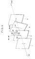
- Fig. 4 illustrates an FLC device having polarizing elements positioned in crossed nicols. In the figure, incident light Ein goes through a
polarizer 1 to become polarized light E1, which goes into anFLC layer 2 having an effect equivalent to that of a halfwave plate. The direction of the polarization of the incident light E1 is the same as that of theaxis 45 of the FLC molecules in one of the two stable state. Ananalyzer 3 is positioned perpendicular to thepolarizer 1. AnotherFLC molecule axis 46 is that of the other stable state. Themolecule axes aligning axis 44, for example, determined by the rubbing method. When the FLC molecules are in onestable state 45, the polarized light is not rotated by theFLC layer 2 and thus entirely blocked byanalyzer 3. Black is thus expressed. When the FLC molecules are in the otherstable state 46, the polarized light is rotated 4ϑc by theFLC layer 2, and then it is transmitted by theanalyzer 3 at a ratio of

white is thus expressed. - Cone angles ϑc in bistable FLC devices are substantially dependent on temperature. Thus, even if a device is positioned as shown in Fig. 1 at one temperature, the
FLC molecule axis 45 in one of the two stable states tilts from the polarization direction of incident light at another temperature because of a change in cone angle. In such a case, the polarized light is rotated by the polarization effect of the FLC layer. Therefore, the contrast degrades because black is not fully expressed in the case where thepolarizer 1 and theanalyzer 3 are positioned in crossed nicols, or because white is not fully expressed in the case where they are positioned in parallel nicols. - It is an object of the present invention to solve the above mentioned problems by providing an optical modulating device in which contrast degradation is substantially reduced.
- In order to achieve the object, the present invention provides an optical modulating device which comprises a polarizer, an analyzer, and liquid crystals positioned between the polarizer and the analyzer, and which controls the birefringence of the liquid crystal by applying an electric field to the liquid crystals so as to change the polarization of light of the device, and which further comprises a rotatable halfwave plate being positioned between the liquid crystals and the analyzer of between the liquid crystals and the polarizer in such a manner that the optical axis of the halfwave plate will be rotated around the optical axis of a display apparatus employing the optical modulating device, and wherein the rotational angle of the halfwave plate is varied in accordance with the temperature of the liquid crystals or the environment thereof, and particularly such angles have one-to-one correspondence to such temperature.
- In the construction as described above, when a proper corresponding relation is set between the rotational angle of the halfwave plate and the temperature of the liquid crystals or its environment, the display conditions in one of the two stable states of the liquid crystals are not affected by a change in cone angles caused by the temperature change. In other words, a constant transmittance can be maintained.
- Ferroelectric liquid crystals (FLCs) may be used as the liquid crystals.
- An optical modulating device according to the present invention may have one of two main constructions. In the first construction, the transmission axes of the polarizer and the analyzer are perpendicular to each other, and the transmission axis of the polarizer is parallel to the FLC molecule axes in one of the two stable states of the FLCs. In the second construction, the transmission axes of the polarizer and the analyzer are parallel to each other, and as in the first construction, the transmission axis of the polarizer is parallel to the FLU molecule axes in one of the two stable states of the FLCs. In either construction, in one of the two stable states, the affection which a cone angle of the FLCs shifted by a temperature change has onto the polarization of the incoming light is cancelled by the polarization effect provided by the accordingly tilted halfway plate, and thus the direction in which incident light is polarized is not rotated, in total, by the polarization. Thus, in one of the two stable states of the FLCs, complete black or complete white can be expressed in spite of the temperature change, so that images with a high contrast can be displayed.
-
- Fig. 1 is a schematic sectional view of an optical modulating device according to an embodiment of the present invention;
- Fig. 2 is a schematic perspective view of the optical modulating device shown in Fig. 1 illustrating the state of each layer thereof at a standard temperature.
- Fig. 3 is a schematic perspective view of the optical modulating device shown in Fig. 1, illustrating the state of each layer thereof at a temperature other than the standard temperature; and
- Fig. 4 is a schematic perspective view of a conventional optical modulating device, illustrating the state of each layer thereof.
- Embodiments of the present invention will be described hereinafter with reference to the figures.
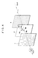
- With reference to Fig. 1, a
polarizer 1 linearly polarizes incident natural light. AnFLC layer 2 controls the state of polarization of incoming linearly polarized light (modulates the light) in accordance with an applied voltage. Ananalyzer 3 transmits only a component of the light modulated by theFLC layer 2, such component having a specified direction. A signal conversion circuit 4 includes a ROM storing a table in which rotational angles correspond to temperatures. Ahalfwave plate 5 is rotatable. TheFLC layer 2 is composed of a pair oftransparent base boards FLC molecule layer 22 provided between thebase boards temperature detector 24 of theFLC molecule layer 22. - Incident light is linearly polarized by the
polarizer 1 and then is modulated byFLC 2. After the modulated light goes through thehalfwave plate 5, it goes into theanalyzer 3, which transmits only a component light in the transmission direction thereof. TheFLC molecule layer 22 exhibits one of the two stable states according to the direction of the electric field applied thereto by transparent electrodes (not shown) formed on the insides of thebase board - The
temperature detector 24 detects the temperature of theFLC molecule layer 22 and its environment. The temperature values are converted by the signal conversion circuit 4 into signals whcih control the rotation of thehalfwave plate 5. - Figs. 2 and 3 illustrate the state of each layer of the optical modulating device at different temperatures A and B, respectively. In the figures, 44 denotes an aligning axis for the FLC molecules, and the angles spreading clockwise with respect to the direction in which the light along the optical axis travels are expressed by negative values.
- Referring to Figs. 2,
FLC molecules axes aligning axis 44 at the temperature A. Incident unpolarized light Ein is polarized by thepolarizer 1, so that the polarized light goes into theFLC layer 2 with the polarization direction of the light being in the direction of themolecule axis 45 at the cone angle +ϑc. When no electric field is applied to theFLC layer 2, the FLC molecule axis is in thedirection 45. In such a case, the polarized light is not rotated by the polarizing effect of theFLC layer 2, nor by the polarizing effect of thehalfwave plate 5, and then is entirely blocked byanalyzer 3. Thus, complete black is expressed. When an electric field is applied to the FLC layer, the FLC molecule axis is in thedirection 46. In this case, the polarized light is rotated -4ϑc by theFLC layer 2 having an effect equivalent to that of a halfwave plate, and then is rotated 8ϑc by thehalfwave plate 5. Thus, the total polarizing rotation by theFLC layer 2 and thehalfwave plate 5 is 4ϑc. Therefore, as in the conventional art, the light is transmitted by the analyzer at a ratio of

- Referring to Fig. 3, when the temperature of the FLC is B, FLC molecule axes 42 and 43 in the two stable states are at cone angles +ϑc' and -ϑc' respectively to the aligning
axis 44, and thehalfwave plate 5 is rotated -(ϑc - ϑc') from the position thereof at the temperature A shown in Fig. 2. As in the case where the temperature is A, incident unpolarized light is polarized by thepolarizer 1, so that the polarized light goes into theFLC layer 2 with the polarization direction of the light being in the direction 45 (shown in Fig. 2). which is at an angle ϑc to the aligningaxis 44. When no electric field is applied to theFLC layer 2, the FLC molecule axis is in thedirection 42. In such a case, the polarized light is rotated -2(ϑc - 0c') across themolecule axis 42 by the polarizing effect of the FLC layer, and then is rotated 2(ϑc - ϑc'), in the opposite direction, by the polarizing effect of thehalfwave plate 5, which is rotated -(ϑc - ϑc') as described above. The two polarizing rotatione effect each other. Therefore, the light coming out of the halfwave plate is entirely blocked by theanalyzer 3. Thus, complete black is expressed. When an electric field is applied to theFLC layer 2, the FLC molecule axis is in thedirection 43. The polarized light is rotated - 2(ϑc' ' ϑc) by theFLC layer 2, and then is rotated (6ϑc' + 2ϑc) in the opposite direction by thehalfwave plate 5. Thus, the total polarizing rotation becomes 4ϑc'. Thus, the total polarizing rotation becomes 4ϑc'. The light is transmitted by the analyzer at a ratio of

- As described above, black is expressed in the constant state in spite of the temperature change. Thus, an optical modulating device according to this embodiment provides high-quality images with a high contrast in a wide temperature range.
- An element in the signal conversion circuit is not necessarily a ROM but may be another element having functions equivalent to those of the ROM
- This embodiment differs from the
embodiment 1 in that apolarizer 1 and ananalyzer 3 are positioned so that the transmission axes thereof are parallel with each other and are parallel with the FLC molecule axis in one of the two stable states. - The incoming polarized light is rotated by the polarizing effect of the FLC layer and the halfwave plate in the same manner as in the
embodiment 1. When there is no electric field applied to the FLC layer, theanalyzer 3 transmits the polarized light entirely. Thus, complete white is expressed. The direction of the polarization completely coincides with the transmission axis at the analyzer, in spite of the temperature change. - Thus, this embodiment provides an optical modulating device which displays high-quality images with a high contrast in a wide temperature range.
- Although the polarizer and the analyzer in the
embodiment - According to this embodiment, the
FLC layer 2 and thehalfwave plate 5 in theembodiments - According to this embodiment, the
rotatable halfwave plate 5 in the above embodiments is substantially a circle which externally touches the four corners of the quadrangular-shapedFLC layer 2, or it is substantially a quadrangle which externally touches such a circle. In this manner, all the light coming out of theFLC layer 2 goes into thehalfwave plate 5, or all the light coming out of thehalfwave plate 5 goes into theFLC layer 2 in the case where they are positioned as in theembodiment 3. - Although the present invention is applied to an optical modulating device using bistable FLCs in the above description, the present invention may be applied to optical modulating devices which are other types of liquid crystals since such devices have substantially the same problems as described above. In such cases, the present invention will provide substantially the same effect as described above.
- Being constructed as described above, an optical modulating device according to the present invention provides a constant contrast or a high transmittance in spite of a change in the temperature of the FLC layer and thus displays high-quality images.
- An optical modulating device comprises a polarizer, an analyzer and liquid crystals positioned between the polarizer and the analyzer. The device controls the birefringence of the liquid crystals by applying an electric field to the liquid crystals so as to change the polarization of light of the device. The device further comprises a rotatable halfwave plate which is positioned between the liquid crystals and the analyzer or between the liquid crystals and the polarizer in such a manner that the optical axis of the halfwave plate will be rotated around the optical axis of light coming into the optical modulating device. The device varies the rotational angle of the halfwave plate in accordance with the temperature of the liquid crystals or the environment thereof.
Claims (4)
- An optical modulating device which comprises a polarizer, an analyzer, and liquid crystals positioned between said polarizer and said analyzer, and which controls the birefringence of said liquid crystals by applying an electric field to said liquid crystals so as to change the polarization of light of said device, further comprising:
a rotationable halfwave plate which is positioned between said liquid crystals and said analyzer or between said liquid crystals and said polarizer in such a manner that the optical axis of said halfwave plate will be rotated around the optical axis of light coming into said optical modulating device,
wherein rotational angles of said halfwave plate have one-to one correspondence to temperature of said liquid crystals or the environment thereof. - An optical modulating device according to claim 1, wherein said liquid crystals are ferroelectric liquid crystals.
- An optical modulating device which comprises a polarizer, an analyzer, and liquid crystals positioned between said polarizer and said analyzer, and which controls the birefringence of said liquid crystals by applying an electric field to said liquid crystals so as to change the polarization of light of said device, further comprising:
a rotatable halfwave plate which is positioned between said liquid crystals and said analyzer or between said liquid crystals and said polarizer in such a manner that the optical axis of said halfwave plate will be rotated around the optical axis of light coming into said optical modulating device,
wherein the rotational angle of said halfwave plate is varied in accordance with the temperature of said liquid crystals or the environment thereof. - An optical modulating device according to claim 3, wherein said liquid crystals are ferroelectric liquid crystals.
Applications Claiming Priority (2)
| Application Number | Priority Date | Filing Date | Title |
|---|---|---|---|
| JP314245/90 | 1990-11-21 | ||
| JP2314245A JP2772582B2 (en) | 1990-11-21 | 1990-11-21 | Optical modulator |
Publications (3)
| Publication Number | Publication Date |
|---|---|
| EP0487047A2 true EP0487047A2 (en) | 1992-05-27 |
| EP0487047A3 EP0487047A3 (en) | 1992-10-14 |
| EP0487047B1 EP0487047B1 (en) | 1997-03-05 |
Family
ID=18051038
Family Applications (1)
| Application Number | Title | Priority Date | Filing Date |
|---|---|---|---|
| EP91119758A Expired - Lifetime EP0487047B1 (en) | 1990-11-21 | 1991-11-19 | Optical modulating device |
Country Status (6)
| Country | Link |
|---|---|
| US (1) | US5257123A (en) |
| EP (1) | EP0487047B1 (en) |
| JP (1) | JP2772582B2 (en) |
| AT (1) | ATE149698T1 (en) |
| CA (1) | CA2055868C (en) |
| DE (1) | DE69124928T2 (en) |
Cited By (4)
| Publication number | Priority date | Publication date | Assignee | Title |
|---|---|---|---|---|
| FR2726919A1 (en) * | 1994-11-14 | 1996-05-15 | Thomson Lcd | LIQUID CRYSTAL DISPLAY DEVICE USING BIREFRINGENT FILMS |
| EP0890864A1 (en) * | 1996-03-29 | 1999-01-13 | Citizen Watch Co. Ltd. | Liquid crystal display |
| WO2003027756A1 (en) * | 2001-09-27 | 2003-04-03 | 3M Innovative Properties Company | Polarization rotators, articles containing polarization rotators, and methods for making and using the same |
| EP1523198A3 (en) * | 2003-10-06 | 2006-11-22 | Seiko Epson Corporation | Optical assembly and projector |
Families Citing this family (8)
| Publication number | Priority date | Publication date | Assignee | Title |
|---|---|---|---|---|
| JP3039570B2 (en) * | 1991-06-24 | 2000-05-08 | キヤノン株式会社 | Projection display device |
| US5870159A (en) * | 1995-10-30 | 1999-02-09 | Kaj | Switchable achromatic polarization rotator |
| US6141071A (en) * | 1995-10-30 | 2000-10-31 | Colorlink, Inc. | Switchable achromatic polarization rotator |
| JP2000347177A (en) * | 1999-03-29 | 2000-12-15 | Minolta Co Ltd | Display optical device and projector display device using the same |
| US6853413B2 (en) * | 2000-04-18 | 2005-02-08 | Honeywell International Inc. | Polarized display with wide-angle illumination |
| JP4822432B2 (en) * | 2006-07-25 | 2011-11-24 | 日東電工株式会社 | Liquid crystal panel and liquid crystal display device |
| US7751109B1 (en) * | 2006-09-14 | 2010-07-06 | The United States Of America As Represented By The Secretary Of The Army | Electro-optic shutter |
| CN110007496B (en) * | 2019-04-17 | 2020-11-27 | 京东方科技集团股份有限公司 | Transparent display device, manufacturing method and driving method thereof, and temperature sensing window |
Citations (4)
| Publication number | Priority date | Publication date | Assignee | Title |
|---|---|---|---|---|
| JPS62204229A (en) * | 1986-03-04 | 1987-09-08 | Casio Comput Co Ltd | Liquid crystal device |
| JPS62247333A (en) * | 1986-04-21 | 1987-10-28 | Seiko Epson Corp | Ferroelectric liquid crystal optical display device |
| JPH01219821A (en) * | 1988-02-29 | 1989-09-01 | Seiko Epson Corp | Liquid crystal optical shutter |
| JPH02828A (en) * | 1987-12-02 | 1990-01-05 | Matsushita Electric Ind Co Ltd | Liquid crystal display device |
Family Cites Families (9)
| Publication number | Priority date | Publication date | Assignee | Title |
|---|---|---|---|---|
| GB2090440A (en) * | 1980-12-16 | 1982-07-07 | Ebauchesfabrik Eta Ag | A watch having an analog display and a digital display |
| JPS6275418A (en) * | 1985-09-27 | 1987-04-07 | Alps Electric Co Ltd | Liquid crystal element |
| EP0263225B1 (en) * | 1986-10-07 | 1992-04-08 | S.A.R.L. S.T. Lagerwall | A device for submicrosecond electro-optic modulation in the liquid crystal smectic-a phase |
| JPS63202717A (en) * | 1987-02-19 | 1988-08-22 | Fujitsu Ltd | Liquid crystal display device |
| JPH01271729A (en) * | 1988-04-25 | 1989-10-30 | Matsushita Electric Ind Co Ltd | Liquid crystal display device |
| JPH024220A (en) * | 1988-06-21 | 1990-01-09 | Seiko Instr Inc | Liquid crystal device |
| JP2861004B2 (en) * | 1988-11-25 | 1999-02-24 | セイコーエプソン株式会社 | Liquid crystal electro-optical device |
| JPH02308219A (en) * | 1989-05-24 | 1990-12-21 | Seiko Epson Corp | Liquid crystal electrooptical element |
| JPH03118513A (en) * | 1989-09-29 | 1991-05-21 | Sharp Corp | Liquid crystal display device |
-
1990
- 1990-11-21 JP JP2314245A patent/JP2772582B2/en not_active Expired - Fee Related
-
1991
- 1991-11-19 DE DE69124928T patent/DE69124928T2/en not_active Expired - Fee Related
- 1991-11-19 EP EP91119758A patent/EP0487047B1/en not_active Expired - Lifetime
- 1991-11-19 AT AT91119758T patent/ATE149698T1/en active
- 1991-11-20 US US07/795,047 patent/US5257123A/en not_active Expired - Fee Related
- 1991-11-20 CA CA002055868A patent/CA2055868C/en not_active Expired - Fee Related
Patent Citations (4)
| Publication number | Priority date | Publication date | Assignee | Title |
|---|---|---|---|---|
| JPS62204229A (en) * | 1986-03-04 | 1987-09-08 | Casio Comput Co Ltd | Liquid crystal device |
| JPS62247333A (en) * | 1986-04-21 | 1987-10-28 | Seiko Epson Corp | Ferroelectric liquid crystal optical display device |
| JPH02828A (en) * | 1987-12-02 | 1990-01-05 | Matsushita Electric Ind Co Ltd | Liquid crystal display device |
| JPH01219821A (en) * | 1988-02-29 | 1989-09-01 | Seiko Epson Corp | Liquid crystal optical shutter |
Non-Patent Citations (4)
| Title |
|---|
| PATENT ABSTRACTS OF JAPAN vol. 12, no. 123 (P-690)16 April 1988 & JP-A-62 247 333 ( SEIKO EPSON ) 28 October 1987 * |
| PATENT ABSTRACTS OF JAPAN vol. 12, no. 62 (P-670)25 February 1988 & JP-A-62 204 229 ( CASIO COMPUT ) 8 September 1987 * |
| PATENT ABSTRACTS OF JAPAN vol. 13, no. 533 (P-967)28 November 1989 & JP-A-1 219 821 ( SEIKO EPSON ) 1 September 1989 * |
| PATENT ABSTRACTS OF JAPAN vol. 14, no. 129 (P-1020)12 March 1990 & JP-A-2 000 828 ( MATSUSHITA ELECTRIC ) 5 January 1990 * |
Cited By (6)
| Publication number | Priority date | Publication date | Assignee | Title |
|---|---|---|---|---|
| FR2726919A1 (en) * | 1994-11-14 | 1996-05-15 | Thomson Lcd | LIQUID CRYSTAL DISPLAY DEVICE USING BIREFRINGENT FILMS |
| WO1996015473A1 (en) * | 1994-11-14 | 1996-05-23 | Thomson-Lcd | Liquid crystal display device using birefringent films |
| EP0890864A1 (en) * | 1996-03-29 | 1999-01-13 | Citizen Watch Co. Ltd. | Liquid crystal display |
| EP0890864A4 (en) * | 1996-03-29 | 2000-08-09 | Citizen Watch Co Ltd | Liquid crystal display |
| WO2003027756A1 (en) * | 2001-09-27 | 2003-04-03 | 3M Innovative Properties Company | Polarization rotators, articles containing polarization rotators, and methods for making and using the same |
| EP1523198A3 (en) * | 2003-10-06 | 2006-11-22 | Seiko Epson Corporation | Optical assembly and projector |
Also Published As
| Publication number | Publication date |
|---|---|
| EP0487047A3 (en) | 1992-10-14 |
| CA2055868A1 (en) | 1992-05-22 |
| EP0487047B1 (en) | 1997-03-05 |
| CA2055868C (en) | 1996-07-02 |
| US5257123A (en) | 1993-10-26 |
| JPH04186224A (en) | 1992-07-03 |
| DE69124928D1 (en) | 1997-04-10 |
| JP2772582B2 (en) | 1998-07-02 |
| ATE149698T1 (en) | 1997-03-15 |
| DE69124928T2 (en) | 1997-07-10 |
Similar Documents
| Publication | Publication Date | Title |
|---|---|---|
| EP0352724B1 (en) | A liquid crystal display device | |
| KR100239266B1 (en) | Optical compensator for liquid crystal display | |
| EP0091637A2 (en) | Liquid crystal display | |
| EP0487047B1 (en) | Optical modulating device | |
| US3915554A (en) | Liquid crystal display device with controllable color | |
| US6067142A (en) | Vertically aligned pi-cell LCD having on-state with mid-plane molecules perpendicular to the substrates | |
| KR100487691B1 (en) | Ferroelectric Liquid Crystal Display | |
| KR100290695B1 (en) | Liquid crystal display device | |
| EP0448173B1 (en) | Liquid crystal display device | |
| JPH04218025A (en) | Reflective type liquid crystal electrooptical element | |
| KR20010042712A (en) | Improved lcd screen viewing angle | |
| JPH0222A (en) | Liquid crystal display panel | |
| JP2898501B2 (en) | Liquid crystal display | |
| JP2789595B2 (en) | Liquid crystal electro-optical element | |
| JPH035721A (en) | Liquid crystal display element | |
| JPH06281927A (en) | Liquid crystal display device | |
| KR20000055745A (en) | Vertical alignment liquid crystal display with wide vieniry angle | |
| JP3090020B2 (en) | Liquid crystal display device | |
| JP2877152B2 (en) | LCD display | |
| JPH08292429A (en) | Liquid crystal display device | |
| KR100658527B1 (en) | Liquid crystal display of in-plane-switching mode and driving method thereof | |
| KR980010521A (en) | Liquid crystal display element | |
| KR100543022B1 (en) | Liquid crystal display | |
| KR100674231B1 (en) | Fringe field switching mode lcd | |
| JP2755428B2 (en) | Reflective liquid crystal display |
Legal Events
| Date | Code | Title | Description |
|---|---|---|---|
| PUAI | Public reference made under article 153(3) epc to a published international application that has entered the european phase |
Free format text: ORIGINAL CODE: 0009012 |
|
| AK | Designated contracting states |
Kind code of ref document: A2 Designated state(s): AT BE CH DE DK ES FR GB GR IT LI LU NL SE |
|
| PUAL | Search report despatched |
Free format text: ORIGINAL CODE: 0009013 |
|
| AK | Designated contracting states |
Kind code of ref document: A3 Designated state(s): AT BE CH DE DK ES FR GB GR IT LI LU NL SE |
|
| 17P | Request for examination filed |
Effective date: 19930224 |
|
| 17Q | First examination report despatched |
Effective date: 19950317 |
|
| GRAG | Despatch of communication of intention to grant |
Free format text: ORIGINAL CODE: EPIDOS AGRA |
|
| GRAH | Despatch of communication of intention to grant a patent |
Free format text: ORIGINAL CODE: EPIDOS IGRA |
|
| GRAH | Despatch of communication of intention to grant a patent |
Free format text: ORIGINAL CODE: EPIDOS IGRA |
|
| GRAA | (expected) grant |
Free format text: ORIGINAL CODE: 0009210 |
|
| AK | Designated contracting states |
Kind code of ref document: B1 Designated state(s): AT BE CH DE DK ES FR GB GR IT LI LU NL SE |
|
| PG25 | Lapsed in a contracting state [announced via postgrant information from national office to epo] |
Ref country code: IT Free format text: LAPSE BECAUSE OF FAILURE TO SUBMIT A TRANSLATION OF THE DESCRIPTION OR TO PAY THE FEE WITHIN THE PRESCRIBED TIME-LIMIT;WARNING: LAPSES OF ITALIAN PATENTS WITH EFFECTIVE DATE BEFORE 2007 MAY HAVE OCCURRED AT ANY TIME BEFORE 2007. THE CORRECT EFFECTIVE DATE MAY BE DIFFERENT FROM THE ONE RECORDED. Effective date: 19970305 Ref country code: GR Free format text: LAPSE BECAUSE OF FAILURE TO SUBMIT A TRANSLATION OF THE DESCRIPTION OR TO PAY THE FEE WITHIN THE PRESCRIBED TIME-LIMIT Effective date: 19970305 Ref country code: BE Effective date: 19970305 Ref country code: AT Effective date: 19970305 Ref country code: CH Effective date: 19970305 Ref country code: LI Effective date: 19970305 Ref country code: ES Free format text: THE PATENT HAS BEEN ANNULLED BY A DECISION OF A NATIONAL AUTHORITY Effective date: 19970305 Ref country code: DK Effective date: 19970305 Ref country code: NL Free format text: LAPSE BECAUSE OF FAILURE TO SUBMIT A TRANSLATION OF THE DESCRIPTION OR TO PAY THE FEE WITHIN THE PRESCRIBED TIME-LIMIT Effective date: 19970305 |
|
| REF | Corresponds to: |
Ref document number: 149698 Country of ref document: AT Date of ref document: 19970315 Kind code of ref document: T |
|
| REG | Reference to a national code |
Ref country code: CH Ref legal event code: EP |
|
| REF | Corresponds to: |
Ref document number: 69124928 Country of ref document: DE Date of ref document: 19970410 |
|
| ET | Fr: translation filed | ||
| PG25 | Lapsed in a contracting state [announced via postgrant information from national office to epo] |
Ref country code: SE Effective date: 19970605 |
|
| NLV1 | Nl: lapsed or annulled due to failure to fulfill the requirements of art. 29p and 29m of the patents act | ||
| REG | Reference to a national code |
Ref country code: CH Ref legal event code: PL |
|
| PG25 | Lapsed in a contracting state [announced via postgrant information from national office to epo] |
Ref country code: LU Free format text: LAPSE BECAUSE OF NON-PAYMENT OF DUE FEES Effective date: 19971119 |
|
| PLBE | No opposition filed within time limit |
Free format text: ORIGINAL CODE: 0009261 |
|
| STAA | Information on the status of an ep patent application or granted ep patent |
Free format text: STATUS: NO OPPOSITION FILED WITHIN TIME LIMIT |
|
| 26N | No opposition filed | ||
| REG | Reference to a national code |
Ref country code: GB Ref legal event code: IF02 |
|
| PGFP | Annual fee paid to national office [announced via postgrant information from national office to epo] |
Ref country code: FR Payment date: 20021108 Year of fee payment: 12 |
|
| PGFP | Annual fee paid to national office [announced via postgrant information from national office to epo] |
Ref country code: GB Payment date: 20021113 Year of fee payment: 12 |
|
| PGFP | Annual fee paid to national office [announced via postgrant information from national office to epo] |
Ref country code: DE Payment date: 20021121 Year of fee payment: 12 |
|
| PG25 | Lapsed in a contracting state [announced via postgrant information from national office to epo] |
Ref country code: GB Free format text: LAPSE BECAUSE OF NON-PAYMENT OF DUE FEES Effective date: 20031119 |
|
| PG25 | Lapsed in a contracting state [announced via postgrant information from national office to epo] |
Ref country code: DE Free format text: LAPSE BECAUSE OF NON-PAYMENT OF DUE FEES Effective date: 20040602 |
|
| GBPC | Gb: european patent ceased through non-payment of renewal fee |
Effective date: 20031119 |
|
| PG25 | Lapsed in a contracting state [announced via postgrant information from national office to epo] |
Ref country code: FR Free format text: LAPSE BECAUSE OF NON-PAYMENT OF DUE FEES Effective date: 20040730 |
|
| REG | Reference to a national code |
Ref country code: FR Ref legal event code: ST |