EP0486865B1 - Higher order phase locked loop - Google Patents
Higher order phase locked loop Download PDFInfo
- Publication number
- EP0486865B1 EP0486865B1 EP91118773A EP91118773A EP0486865B1 EP 0486865 B1 EP0486865 B1 EP 0486865B1 EP 91118773 A EP91118773 A EP 91118773A EP 91118773 A EP91118773 A EP 91118773A EP 0486865 B1 EP0486865 B1 EP 0486865B1
- Authority
- EP
- European Patent Office
- Prior art keywords
- path
- phase
- locked loop
- operational amplifier
- integrator
- Prior art date
- Legal status (The legal status is an assumption and is not a legal conclusion. Google has not performed a legal analysis and makes no representation as to the accuracy of the status listed.)
- Expired - Lifetime
Links
Images
Classifications
-
- H—ELECTRICITY
- H03—ELECTRONIC CIRCUITRY
- H03L—AUTOMATIC CONTROL, STARTING, SYNCHRONISATION, OR STABILISATION OF GENERATORS OF ELECTRONIC OSCILLATIONS OR PULSES
- H03L7/00—Automatic control of frequency or phase; Synchronisation
- H03L7/06—Automatic control of frequency or phase; Synchronisation using a reference signal applied to a frequency- or phase-locked loop
- H03L7/08—Details of the phase-locked loop
- H03L7/085—Details of the phase-locked loop concerning mainly the frequency- or phase-detection arrangement including the filtering or amplification of its output signal
- H03L7/093—Details of the phase-locked loop concerning mainly the frequency- or phase-detection arrangement including the filtering or amplification of its output signal using special filtering or amplification characteristics in the loop
-
- H—ELECTRICITY
- H04—ELECTRIC COMMUNICATION TECHNIQUE
- H04L—TRANSMISSION OF DIGITAL INFORMATION, e.g. TELEGRAPHIC COMMUNICATION
- H04L27/00—Modulated-carrier systems
- H04L27/32—Carrier systems characterised by combinations of two or more of the types covered by groups H04L27/02, H04L27/10, H04L27/18 or H04L27/26
- H04L27/34—Amplitude- and phase-modulated carrier systems, e.g. quadrature-amplitude modulated carrier systems
- H04L27/38—Demodulator circuits; Receiver circuits
- H04L27/3818—Demodulator circuits; Receiver circuits using coherent demodulation, i.e. using one or more nominally phase synchronous carriers
- H04L27/3827—Demodulator circuits; Receiver circuits using coherent demodulation, i.e. using one or more nominally phase synchronous carriers in which the carrier is recovered using only the demodulated baseband signals
Definitions
- the invention relates to a higher order phase locked loop with automatic residual error compensation according to the preamble of claim 1.
- Phase control loops of the aforementioned type are from the book by F. Gardner, Phaselock-Techniques, publisher John Wiley 1966, ISBN 0-471-04294-3, or from the book by Roland Best, theory and applications of the Phaselocked Loops, AT-Verlag, Aarau (Switzerland) 1981, ISBN 3-85502-123-6 known.
- Higher-order phase locked loops (0 ⁇ 2) as they are e.g. B. used in multistage QAM systems for carrier and / or clock recovery, must have a very small residual control error, so that an optimal sampling window for the signal decision is created.
- the task of carrier recovery is, for example, to position the constellation points as precisely as possible on a square pattern. If there is an alignment error of only 1 degree, a 64QAM system degrades by 0.85 dB and a 256 QAM system by 2 dB at a bit error rate of 10exp-9.
- a control error leads to an incorrectly selected sampling time ("the eye is not hit"), which quickly becomes disruptive, particularly in systems without a time domain equalizer B. Notch on the Nyquist frequency) prevent the loop from re-engaging.
- DSPs signal processors
- the invention has for its object to provide a phase-locked loop in which the above-described difficulties are eliminated.
- phase control loops of higher order depends on circuit properties such as component tolerances, offset, temperature drift and aging on the one hand and the frequency offset of the recovered signal on the other. This leads to phase locked loops, such as those used for. B. in higher-level QAM systems for clock and carrier recovery, to reduce the sampling window in the signal decision and thus the system gain.
- the circuit according to the invention automatically adjusts the residual error during operation. The above problems are avoided. No adjustment is required when testing the circuit.
- the specified circuit principle can therefore basically be applied to all phase-locked loops, provided that a binary, that is to say a digital, error criterion can be derived at the control target.
- FIG. 1 shows the circuit principle known per se, as is also analogously from the book F. Gardner, Phaselock-Techniques, publisher John Wiley 1966, ISBN 0-471-04294-3 or from the book R. Best, theory and applications of the Phaselocked Loops, AT publishing house, Aarau (Switzerland) 1981, ISBN 3-85502-123-6 is known.
- VCO voltage controlled oscillator
- phase detector which derives the correct phase for QAM demodulation.
- the input signals are, so to speak, designated QAM, which are known as I, Q signals. are divided.
- the phase detector is followed by a delay element with the delay time T, it is followed by a low-pass filter (with a dashed frame) TP and a further circuit section with a dashed frame, which is referred to as an LF (loop filter).
- LF loop filter
- the low-pass filter TP which can generally be neglected for the entire transfer function in the region of interest, consists of a half element with the series resistor R3 to which a capacitor C3 is connected in the direction of earth (ground).
- the loop filter LF shows an operational amplifier whose non-inventorying input (+) is connected to ground and whose inverting input is connected upstream of resistor R1 and whose output is connected in parallel from resistor R8 and the series circuit from resistor R2 and Capacitor C2 is connected to the inverting input (-).
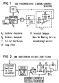
- FIG. 1 shows the basic circuit diagram of a second-order phase locked loop, as has been the case up to now in QAM demodulators for radio relay systems with high bandwidth efficiency.
- the low-pass filter TP has the task of keeping high-frequency voltage peaks away from the subsequent operational amplifier. Due to its relatively high cut-off frequency compared to the cut-off frequency of the loop filter, it practically does not enter into the phase transfer function. In practical application, the parts LF and TP are designed symmetrically for circuit stability.
- the dead time T which e.g. created by the runtime in the time domain equalizer is meaningless in this context. It is only included for the sake of completeness.
- the offset problem of the overall circuit can be reduced to a single offset voltage, which is impressed at point A. In practice, this offset voltage must be exactly balanced and maintain its value over temperature and time.
- Resistor R8 results in a proportional control component in the transfer function, which then leads to a stationary control residual error if the frequency of the signal to be detected does not correspond to the VCO center frequency. It is therefore made as large as possible. However, it is for re-engagement - e.g. after signal interruptions - unavoidable, since without it the operational amplifier would run to a stop in the disengaged state and would lose the transmission properties necessary for re-engagement.
- the new circuit described here bypasses the resistor R8 and the problems associated with it on the one hand and on the other hand ensures an automatic continuous offset adjustment during operation.
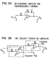
- FIG. 2 shows the automatic offset adjustment using the example of the coefficient control of an adaptive time domain equalizer with auto-zero technology.
- You can see a Actuator followed by a digital criterion (ex-or gate), the output of which leads to a switch S1.
- a reference bit sequence is fed to a second input of the switch S1.
- a refresh generator controls switches S1 and S2.
- a capacitor C H can be seen , which is connected on the one hand to the non-inverting input of an operational amplifier (op-amp) and on the other hand to ground.
- the output of the op-amp is fed back via the capacitor C4 and is connected there to the inverting input of the op-amp.
- This T-element leads on the input side to the resistor R3 connected upstream of the switch S2.
- the output of the op-amp is switched to the input of the actuator.
- the reference bit sequence is periodically switched via a series resistor and S2 (bidirectional C-MOS switch) to a holding capacitor C H , which is located directly at the reference voltage input of the integrator (J-FET op-amp) and which is based on the mean value voltage of only the reference sequence and does not set the result bit sequence.
- This mean value voltage represents the reference zero voltage of the integrator in a practically ideal manner when the value has disappeared Correlation in the result bit sequence is independent of the physical level changes of the digital signal, temperature, aging and delivery tolerances.
- the low pass R1 / C2 in turn suppresses the high frequency components in front of the op-amp.
- R2 / C4 determine the intergrinding constant (1 / 0.5 ms was selected)
- the control circuit represents (if neglecting R1 / C2) a first-order control circuit.
- the 3 dB limit frequency (closed loop bandwidth) is a few kilohertz. It is fast enough to set the equalizer coefficients.
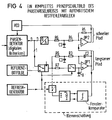
- FIG. 3A can be recognized as a classic loop filter in FIG. 1.
- Figure 3B shows the disassembled structure of the loop filter.
- the input is labeled U e1 and the output is labeled U a2 .
- the slow path consists of an operational amplifier, which is fed back via a capacitor C2 and whose inverting input is preceded by the resistor R3.
- the non-inverting input is grounded.
- the quick path is there likewise from an operational amplifier, the non-inverting input of which is supplied with the signal U x coming from the slow path.
- the output of this operational amplifier is switched back via the resistor R5 at the inverting input, which in turn is connected to the resistor R4.
- a line leads from the input U e1 to the resistor R4.
- the denominator of the equations is found.
- the slow path is an integrator with the integrator constant 1 / (R3 * C2). In practical applications (e.g. carrier recovery), this constant is significantly smaller than the 3 dB bandwidth of the entire loop.
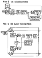
- Figure 4 shows the complete block diagram of the phase-locked loop with automatic residual error compensation.
- the subcircuits explained at the beginning can be seen.
- the subdivision "fast path” and “slow path” is adhered to.
- An operational amplifier OP2 is assigned to the fast path and an operational amplifier OP1 to the slow path.
- the individual circuit components have been described above.
- a D / A converter DA .. is connected upstream of the fast path.
- the phase detector (digital criterion), the reference bit sequence and a refresh generator can be seen.
- the dashed-framed circuit which is referred to as the clamping circuit, is also assigned.
- This clamp circuit contains a window comparator and a controlled current source.
- the output of the fast path leads to the voltage controlled oscillator VCO.
- the output of the slow path leads to the clamp circuit and to the input of the fast path.
- FIG. 4 shows the overall circuit.
- the clamping circuit is discussed in the next section.
- R6 and C3 again serve to suppress high-frequency interference.
- the phase detector criterion is taken from the output of a digital module. If the word width of the detector signal is more than one bit, only the most significant bit is fed to the slow path. The full word width can then be converted into an analog signal in the fast path using a D / A converter, which can have a particularly favorable effect on low residual control noise and greater independence of the 3 dB bandwidth of the loop from the signal-to-noise ratio.
- the resistor R8 is required in the feedback path of the op-amp, which, however, causes static residual control errors in the case of frequency deposits.
- the clamp circuit also shown avoids this disadvantage.
- the integrator output voltage will try to run to the stop.
- the window comparator detects whether this voltage exceeds predetermined upper and lower limits. These limits set the maximum frequency range of the circuit.
- a positive or negative clamp current is fed into the integrator via a current source. This prevents OP1 from going outside its output voltage operating range.
- the loop is closed, the frequency locking process can begin immediately.
- a circuit element corresponding to the resistor R8 is therefore not required in the entire circuit. As a result, the same residual phase error accuracy is achieved with all frequency offsets (of the VCO) as described above.
- the clamping circuit can be easily expanded to a frequency search circuit (wobbler) if the two thresholds of the window comparator are set or reset in flip-flop and the output of the flip-flop determines the compensation current. Compare claim 5.
- FIG. 5 and 6 show application examples of the principle, specifically in FIG. 5 an example for carrier recovery and in FIG. 6 an example for clock recovery.
- a voltage-dependent oscillator VCO can be seen with the 0 ° and the 90 ° path, a QAM demodulator, from which the signals I and Q are taken and then passed to A / D converters, there follows a digital time domain equalizer (ATDE) and a phase detector and it is then divided into the slow path with auto-zero technology and on the other hand after a D / A converter in the fast path.
- a voltage-dependent oscillator VCO can be seen with the 0 ° and the 90 ° path, a QAM demodulator, from which the signals I and Q are taken and then passed to A / D converters, there follows a digital time domain equalizer (ATDE) and a phase detector and it is then divided into the slow path with auto-zero technology and on the other hand after a D / A converter in the fast path.
- ATDE digital time domain equalizer
- FIG. 6 shows a clock recovery.
- lines there which are crossed out obliquely, and the numbers n and 1-8 mean that there are lines for a data bus with bit n or 1-8 lines.
- FIG. 6 again shows a QAM demodulator with the signals I and Q.
- An A / D converter follows in path I, as does path Q in the same way. Circuit parts follow in both paths, which supply digital clock criteria and finally D / A converter .
- the "slow path (auto-zero technology)" is reached via a multiplexer MUX which processes only the most significant (1) of the data bus (5) and it is processed by the lower D / A converter via a totalizer ⁇ fast path reached.
- the fast path controls the block VCXO (Voltage controlled x-tal oscillator), which in turn provides the clock for the A / D conversion.
- VCXO Voltage controlled x-tal oscillator
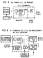
- FIG. 7 shows the principle of the (sigma-delta) D / A conversion in the block diagram.
- the symbols have already been explained on earlier figures.
- a circuit part can be seen which provides a digital criterion and a clock generator (fc >>> f 3dB) whose frequency f c is significantly higher than the 3dB cut-off frequency of the subsequent analog low pass.
- the entire (sigma-delta) D / A converter is divided into a digital part and an analog filter (low pass), with an analog output.
- the digital one Part contains the summer ⁇ , which is followed by an accumulator (accumulator) and whose most significant bit (MSB) is fed back to the summer ( ⁇ ) and passed into the input of the analog low pass.
- accumulator accumulator
- MSB most significant bit
- the phase detector signal has a word length of several bits and at the same time there is a very large frequency spacing between the highest transmission frequency and the clock frequency
- the previously described carrier and clock recovery circuits (FIGS. 5, 6) can be used instead of an n-bit wide D / A converter the (Sigma-Delta) principle can be used advantageously. This is the case with the examples.
- the principle of the (sigma-delta) D / A conversion is shown in FIG.
- the multi-stage output signal of the digital criterion or the phase detector is fed into the digital part of the (sigma-delta) converter.
- the output of the digital part has only 1-bit word width. Due to the special circuit, however, the spectral components of the noise generated by the 1-bit quantization are very low at low frequencies, so that after the subsequent analog low-pass filter, which in turn suppresses the strong high-frequency components, very little residual noise remains.
- the digital part can be easily implemented as an additional function in a digital module and the output signal then requires only a single pin and no additional D / A converter.
- FIG. 7 A combination of the (sigma-delta) D / A converter principle with auto-zero technology is shown in FIG.
- a digital criterion / phase detector can be seen, followed by a broken line, an expanded digital part, which is followed by the "fast path”.
- the VCO is located at its exit.
- the expanded digital part is comparable to FIG. 7, however, additionally contains the circuit section “reference bit sequence”. and a switch module.
- the "slow path, auto-zero path” is reached from the output of the switch module. It contains a "refresh generator” that leads to the switch module on the one hand and to the "slow path, auto-zero” on the other.
- the exit of the slow path leads to another entry of the "fast path”.
- the digital part only has to be expanded slightly and an additional output for the slow path must be provided.
- the circuit almost perfectly combines the advantages of the (sigma-delta) conversion principle with those of auto-zero self-balancing technology in semi-digitally implemented phase-locked loops, especially for clock and carrier recovery in QAM radio relay systems with a high number of modulation stages or high bandwidth efficiency.
Description
Die Erfindung betrifft einen Phasenregelkreis höherer Ordnung mit automatischem Restfehlerabgleich gemäß dem Oberbegriff des Patentanspruchs 1.The invention relates to a higher order phase locked loop with automatic residual error compensation according to the preamble of
Phasenregelkreise der vorgenannten Art sind aus dem Buch von F. Gardner, Phaselock-Techniques, Verlag John Wiley 1966, ISBN 0-471-04294-3, oder aus dem Buch von Roland Best, Theorie und Anwendungen des Phaselocked Loops, A.T.-Verlag, Aarau (Schweiz) 1981, ISBN 3-85502-123-6 bekannt.Phase control loops of the aforementioned type are from the book by F. Gardner, Phaselock-Techniques, publisher John Wiley 1966, ISBN 0-471-04294-3, or from the book by Roland Best, theory and applications of the Phaselocked Loops, AT-Verlag, Aarau (Switzerland) 1981, ISBN 3-85502-123-6 known.
Phasenregelkreise höherer Ordnung (0≥2), wie sie z. B. in vielstufigen QAM-Systemen zur Träger- und/oder Taktrückgewinnung verwendet werden, müssen einen sehr kleinen Regelrestfehler aufweisen, damit ein optimales Abtastfenster für die Signalentscheidung geschaffen wird. Aufgabe der Trägerrückgewinnung ist es beispielsweise, die Konstellationspunkte möglichst exakt auf ein quadratisches Muster zu positionieren. Liegt ein Abgleichfehler von nur 1 Grad vor, so degradiert bei einer Bitfehlerrate von 10exp-9 ein 64QAM-System bereits um 0.85 dB, ein 256 QAM-System um 2 dB. Im Falle des Taktregelkreises führt ein Regelfehler einerseits zu einem falsch gewählten Abtastzeitpunkt ("das Auge wird nicht getroffen"), was insbesondere bei Systemen ohne Zeitbereichsentzerrer sehr schnell störend wird, andererseits wird ein Regelrestfehler (Offset-problem) bei bestimmten Selektiv-Verzerrungen (z. B. Notch auf der Nyquistfrequenz) das Wiedereinrasten der Schleife verhindern.Higher-order phase locked loops (0≥2), as they are e.g. B. used in multistage QAM systems for carrier and / or clock recovery, must have a very small residual control error, so that an optimal sampling window for the signal decision is created. The task of carrier recovery is, for example, to position the constellation points as precisely as possible on a square pattern. If there is an alignment error of only 1 degree, a 64QAM system degrades by 0.85 dB and a 256 QAM system by 2 dB at a bit error rate of 10exp-9. In the case of the clock control loop, on the one hand, a control error leads to an incorrectly selected sampling time ("the eye is not hit"), which quickly becomes disruptive, particularly in systems without a time domain equalizer B. Notch on the Nyquist frequency) prevent the loop from re-engaging.
Um diese Nachteile zu vermeiden, mußte bisher ein sehr genauer Offset-Abgleich des Phasendetektors und des Loopfilters, realisiert mit Hilfe von Operationsverstärkern, durchgeführt werden. Dieser Abgleich muß auch über Temperatur und Alterungstoleranzen stehen bleiben. Insbesondere bei Systemen mit kleinem Roll-off (Rho = 0.2) kann das zur Einführung von Temperaturkompensationen in den Schaltungen führen. Alterungseffekte können jedoch nicht in jedem Fall beseitigt werden.In order to avoid these disadvantages, a very precise offset adjustment of the phase detector and the loop filter, realized with the aid of operational amplifiers, had previously to be carried out. This adjustment also has to be done via temperature and aging tolerances stop. Particularly in systems with a small roll-off (Rho = 0.2), this can lead to the introduction of temperature compensation in the circuits. However, aging effects cannot always be eliminated.
Grundsätzlich ließen sich die obengenannten Nachteile mit volldigital realisierten Schaltungen vermeiden. Aufwandabschätzung vom schnellen, volldigitalen Trägerregelkreisen, ergeben jedoch zu hohe Kosten und lange Entwicklungszeiten.In principle, the above-mentioned disadvantages could be avoided with fully digital circuits. Effort estimate of the fast, fully digital carrier control loops, however, result in high costs and long development times.
Bei ausreichend geringer Verarbeitungsgeschwindigkeit ist eine digitale Realisierung in Signalprozessoren (DSP's) möglich.With a sufficiently low processing speed, digital implementation in signal processors (DSPs) is possible.
Bei analoger Realisierung werden durch symmetrische Schaltungsauslegung, Temperaturkompensation und Präzisionsabgleich die Probleme reduziert. Das bekannte Problem des Restfehlers bei Frequenzversatz des rückgewonnenen Signals wurde wegen des bislang als unvermeidbar angesehenen ohmschen Widerstand in der Rückkopplung des Operationsverstärkers (Propotionalanteil) nicht grundsätzlich gelöst.In the case of analog implementation, the problems are reduced by symmetrical circuit design, temperature compensation and precision adjustment. The known problem of the residual error in the frequency offset of the recovered signal was not fundamentally solved because of the ohmic resistance in the feedback of the operational amplifier (proportional component), which was previously considered unavoidable.
Der Erfindung liegt die Aufgabe zugrunde, einen Phasenregelkreis anzugeben, bei dem die vorstehend geschilderten Schwierigkeiten beseitigt sind.The invention has for its object to provide a phase-locked loop in which the above-described difficulties are eliminated.
Diese Aufgabe wird gemäß der Erfindung nach den kennzeichnenden Merkmalen des Patentanspruchs 1 gelöst.This object is achieved according to the invention according to the characterizing features of
Vorteilhafte Ausführungsformen sind in den Unteransprüchen angegeben.Advantageous embodiments are specified in the subclaims.
Der statische Regelrestfehler von herkömmlichen, analog realierten Phasenregelkreisen höherer Ordnung (0 ≥ 2) hängt von Schaltungseigenschaften wie Bauelementetoleranzen, Offset, Temperaturdrift und Alterung einerseits sowie vom Frequenzversatz des rückgewonnenen Signals andererseits ab. Dies führt bei Phasenregelkreisen, wie sie z. B. bei höherstufigen QAM-Systemen zur Takt- und Trägerrückgewinnung verwendet werden, zu einer Reduktion des Abtastfensters bei der Signalentscheidung und damit des Systemgewinns.The static residual control error of conventional, similarly implemented phase control loops of higher order (0 ≥ 2) depends on circuit properties such as component tolerances, offset, temperature drift and aging on the one hand and the frequency offset of the recovered signal on the other. This leads to phase locked loops, such as those used for. B. in higher-level QAM systems for clock and carrier recovery, to reduce the sampling window in the signal decision and thus the system gain.
Die erfindungsgemäße Schaltung gleicht bei laufendem Betrieb automatisch den Restfehler ab. Die obengenannten Probleme werden damit umgangen. Beim Prüfen der Schaltung ist keinerlei Abgleich erforderlich.The circuit according to the invention automatically adjusts the residual error during operation. The above problems are avoided. No adjustment is required when testing the circuit.
Es läßt sich also das angegebene Schaltungsprinzip grundsätzlich auf alle Phasenregelkreise anwenden, sofern ein binäres, also ein digitales Fehlerkriterium am Regelziel abgeleitet werden kann.The specified circuit principle can therefore basically be applied to all phase-locked loops, provided that a binary, that is to say a digital, error criterion can be derived at the control target.
Anhand von Ausführungsbeispielen wird nachstehend die Erfindung noch näher erläutert.The invention is explained in more detail below on the basis of exemplary embodiments.
Es zeigen:
- Fig. 1
- einen Phasenregelkreis 2. Ordnung, Standard-Schaltung
- Fig. 2
- eine Koeffizienten-Regelung mit Auto-Zero-Technik,
- Fig. 3a
- ein klassisches Loopfilter für Phasenregelkreis 2. Ordnung,
- Fig. 3b
- eine "zerlegte" Struktur des Loopfilters,
- Fig. 4
- ein komplettes Prinzipschaltbild des Phasenregelkreises mit automatischem Restfehlerabgleich,
- Fig. 5
- eine Trägerrückgewinnung,
- Fig. 6
- eine digitale Taktrückgewinnung,
- Fig. 7
- das Prinzip der (Σ-Δ) D/A-Wandlung und
- Fig. 8
- die Kombination des (Σ-Δ) - D/A-Wandler-Prinzip mit der Auto-Zerotechnik.
- Fig. 1
- a 2nd order phase locked loop, standard circuit
- Fig. 2
- a coefficient control with auto-zero technology,
- Fig. 3a
- a classic loop filter for 2nd order phase locked loops,
- Fig. 3b
- a "disassembled" structure of the loop filter,
- Fig. 4
- a complete block diagram of the phase-locked loop with automatic residual error compensation,
- Fig. 5
- a carrier recovery,
- Fig. 6
- digital clock recovery,
- Fig. 7
- the principle of (Σ-Δ) D / A conversion and
- Fig. 8
- the combination of the (Σ-Δ) - D / A converter principle with auto zero technology.
Figur 1 zeigt das an sich bekannte Schaltungsprinzip, wie es sinngemäß auch aus dem Buch F. Gardner, Phaselock-Techniques, Verlag John Wiley 1966, ISBN 0-471-04294-3 oder aus dem Buch R. Best, Theorie und Anwendungen des Phaselocked Loops, A.T.-Verlag, Aarau (Schweiz) 1981, ISBN 3-85502-123-6 bekannt ist.FIG. 1 shows the circuit principle known per se, as is also analogously from the book F. Gardner, Phaselock-Techniques, publisher John Wiley 1966, ISBN 0-471-04294-3 or from the book R. Best, theory and applications of the Phaselocked Loops, AT publishing house, Aarau (Switzerland) 1981, ISBN 3-85502-123-6 is known.
Die in Figur 1 eingeführten Schaltsymbole, Bezeichnungen und Bezugshinweise werden in den folgenden Figuren mit der gleichen Bedeutung wiederverwendet.The circuit symbols, designations and reference notes introduced in FIG. 1 are reused in the following figures with the same meaning.
In Figur 1 ist also zu erkennen ein spannungsgesteuerter Oszillator (VCO) der zur QAM-Demodulation erforderlich ist und einen Phasendetektor der die für die QAM-Demodulation, korrekte Phase ableitet. Die Eingangssignale sind gewissermaßen mit QAM bezeichnet, die dort in bekannter Weise in I, Q-Signale. unterteilt sind. Dem Phasendetektor folgt ein Laufzeitglied mit der Laufzeit T, es schließt sich an ein Tiefpaß (gestrichelt eingerahmt) TP und ein weiterer gestrichelt eingerahmter Schaltungsabschnitt, der als LF (Loop-filter) bezeichnet ist. Wie der Pfeil erkennen läßt, ist die Signalflußrichtung vom Ausgang des Loop-filters LF auf den Eingang des spannungsabhängigen Oszillators VCO, gekennzeichnet durch seine Oszillator-Konstante K₀, gerichtet. Der Tiefpaß TP, der für die gesamte Ubertragungsfunktion im interessierenden Bereich im allgemeinen vernachlässigt werden kann, besteht aus einem Halbglied mit dem Serienwiderstand R3 dem in Richtung Erde (Masse) ein Kondensator C3 zugeschaltet ist. Im Loop-filter LF ist zu erkennen ein Operationsverstärker, dessen nicht inventierender Eingang (+) an Masse geschaltet ist und dessen invertierendem Eingang der Widerstand R1 vorgeschaltet ist und dessen Ausgang über die Parallelschaltung aus dem Widerstand R8 und die Serienschaltung aus dem Widerstand R2 und dem Kondensator C2 mit dem invertierenden Eingang (-) verbunden ist.1 shows a voltage controlled oscillator (VCO) which is required for QAM demodulation and a phase detector which derives the correct phase for QAM demodulation. The input signals are, so to speak, designated QAM, which are known as I, Q signals. are divided. The phase detector is followed by a delay element with the delay time T, it is followed by a low-pass filter (with a dashed frame) TP and a further circuit section with a dashed frame, which is referred to as an LF (loop filter). As the arrow shows, the direction of signal flow from the output of the loop filter LF is directed to the input of the voltage-dependent oscillator VCO, characterized by its oscillator constant K₀. The low-pass filter TP, which can generally be neglected for the entire transfer function in the region of interest, consists of a half element with the series resistor R3 to which a capacitor C3 is connected in the direction of earth (ground). The loop filter LF shows an operational amplifier whose non-inventorying input (+) is connected to ground and whose inverting input is connected upstream of resistor R1 and whose output is connected in parallel from resistor R8 and the series circuit from resistor R2 and Capacitor C2 is connected to the inverting input (-).
Figur 1 zeigt das prinzipielle Schaltbild eines Phasenregelkreises zweiter Ordnung, wie er bislang in QAM-Demodulatoren für Richtfunksysteme mit hoher Bandbreiteneffizienz realisiert wurde. Der Tiefpaß TP hat die Aufgabe, hochfrequente Spannungsspitzen vom nachfolgenden Operationsverstärker fernzuhalten. Aufgrund seiner relativ hohen Grenzfrequenz, verglichen mit der Grenzfrequenz des Loopfilters, geht er praktisch nicht in die Phasen-Übertragungsfunktion ein. In praktischer Anwendung werden zur Schaltungsstabilität die Teile LF und TP symmetrisch ausgeführt.FIG. 1 shows the basic circuit diagram of a second-order phase locked loop, as has been the case up to now in QAM demodulators for radio relay systems with high bandwidth efficiency. The low-pass filter TP has the task of keeping high-frequency voltage peaks away from the subsequent operational amplifier. Due to its relatively high cut-off frequency compared to the cut-off frequency of the loop filter, it practically does not enter into the phase transfer function. In practical application, the parts LF and TP are designed symmetrically for circuit stability.
Die Totzeit T, die z.B. durch Laufzeit im Zeitbereichs-Entzerrer entsteht, ist in diesem Zusammenhang bedeutungslos. Sie ist nur der Vollständigkeit halber mitaufgeführt. Die Offset-Problematik der Gesamtschaltung läßt sich reduzieren auf eine einzige Offsetspannung, die am Punkt A eingeprägt ist. Diese Offsetspannung muß in der Praxis genau abgeglichen sein und ihren Wert über Temperatur und Zeit beibehalten.The dead time T, which e.g. created by the runtime in the time domain equalizer is meaningless in this context. It is only included for the sake of completeness. The offset problem of the overall circuit can be reduced to a single offset voltage, which is impressed at point A. In practice, this offset voltage must be exactly balanced and maintain its value over temperature and time.
Der Widerstand R8 ergibt einen Proportional-Regelanteil in der Übertragungsfunktion, der dann zu einem stationären Regelrestfehler führt, wenn die Frequenz des zu detektierenden Signals nicht der VCO-Mittenfrequenz entspricht. Er wird deshalb so groß wie möglich gemacht. Er ist allerdings für das Wiedereinrasten- z.B. nach Signalunterbrechungen - unumgänglich, da ohne ihn im ausgerasteten Zustand der Operationsverstärker auf Anschlag laufen und damit die für das Wiedereinrasten notwendigen Ubertragungseigenschaften verlieren würde.Resistor R8 results in a proportional control component in the transfer function, which then leads to a stationary control residual error if the frequency of the signal to be detected does not correspond to the VCO center frequency. It is therefore made as large as possible. However, it is for re-engagement - e.g. after signal interruptions - unavoidable, since without it the operational amplifier would run to a stop in the disengaged state and would lose the transmission properties necessary for re-engagement.
Die hier beschriebene neue Schaltung umgeht einerseits den Widerstand R8 und die damit verbundenen Probleme und besorgt andererseits einen automatischen kontinuierlichen Offsetabgleich bei laufendem Betrieb.The new circuit described here bypasses the resistor R8 and the problems associated with it on the one hand and on the other hand ensures an automatic continuous offset adjustment during operation.
In Figur 2 ist der automatische Offset-Abgleich am Beispiel der Koeffizienten-Regelung eines adaptiven Zeitbereichsentzerrers mit Auto-Zero-Technik gezeigt. Zu erkennen ist ein Stellglied, dem ein Digital-Kritierium (Ex-Or Gatter) folgt, dessen Ausgang auf einen Schalter S1 führt. Einem zweiten Eingang des Schalters S1 wird zugeführt eine Referenzbitfolge. Ein Refreshgenerator steuert die Schalter S1 und S2. Zu erkennen ist ein Kondensator CH, der einerseits an dem nichtinvertierenden Eingang eines Operationsverstärkers (Op-Amp) und andererseits an Masse liegt. Der Ausgang des Op-Amps ist rückgekoppelt über den Kondensator C4 und dort mit dem invertierenden Eingang des Op-Amps verbunden. Ein T-Glied mit den Widerständen R1, R2 und dem Kondensator C2 im Querzweig (Masse) überbrückt den Schalter S2. Dieses T-Glied führt eingangsseitig auf den dem Schalter S2 vorgeschalteten Widerstand R3. Der Ausgang des Op-Amps ist auf den Eingang des Stellgliedes geschaltet.FIG. 2 shows the automatic offset adjustment using the example of the coefficient control of an adaptive time domain equalizer with auto-zero technology. You can see a Actuator followed by a digital criterion (ex-or gate), the output of which leads to a switch S1. A reference bit sequence is fed to a second input of the switch S1. A refresh generator controls switches S1 and S2. A capacitor C H can be seen , which is connected on the one hand to the non-inverting input of an operational amplifier (op-amp) and on the other hand to ground. The output of the op-amp is fed back via the capacitor C4 and is connected there to the inverting input of the op-amp. A T-element with the resistors R1, R2 and the capacitor C2 in the shunt arm (ground) bridges the switch S2. This T-element leads on the input side to the resistor R3 connected upstream of the switch S2. The output of the op-amp is switched to the input of the actuator.
Ausgangspunkt der Uberlegungen war das Patent "1 Bit/l Bit Digital-Korrelator mit selbständig einstellender Integrator-Referenzspannung" (EP 0149803). Sie liefert sehr präzise, reproduzierbare Einstellungen ohne Fertigungsprobleme. Figur 2 zeigt das Schaltungsprinzip. Eine Referenzbitfolge wird periodisch über den getakteten Schalter S1 in den vom digitalen Kriterium (Ex-Or-Gatter) kommenden Datenstrom (Ergebnisbitfolge) eingeblendet.The starting point for the considerations was the patent "1-bit / 1-bit digital correlator with independently setting integrator reference voltage" (EP 0149803). It delivers very precise, reproducible settings without manufacturing problems. Figure 2 shows the circuit principle. A reference bit sequence is inserted periodically via the clocked switch S1 into the data stream (result bit sequence) coming from the digital criterion (ex-or gate).
Sie hat den gleichen physikalischen Gleichspannungsmittelwert wie eine Ergebnisbitfolge, bei der Nullen und Einsen mit zufallsartiger Gleichverteilung auftreten. Die Referenzbitfolge wird periodisch über einen Vorwiderstand und S2 (bidirektionaler C-MOS-Schalter) auf einen Haltekondensator CH geschaltet, der unmittelbar am Referenz-Spannungseingang des Integrators (J-FET Op-Amp) liegt und der sich auf die Mittelwertspannung nur der Referenzfolge und nicht der Ergebnisbitfolge einstellt. Diese Mittelwertspannung stellt in praktisch idealer Weise die Referenz-Nullspannung des Integrators bei verschwundener Korrelation in der Ergebnisbitfolge dar und zwar unabhängig von physikalischen Pegeländerungen des Digitalsignals, Temperatur, Alterung und Anliefertoleranzen. Der Tiefpaß R1/C2 unterdrückt wiederum die hohen Frequenz anteile vor dem Op-Amp. R2/C4 bestimmen die Intergratorkonstante (gewählt wurde 1/0.5 ms) Die Regelschaltung stellt (bei Vernachlässigung von R1/C2) einen Regelkreis erster Ordnung dar. Die 3 dB Grenzfrequenz (closed loop bandwidth) liegt bei einigen Kilohertz. Sie ist ausreichend schnell zur Einstellung der Entzerrer-Koeffizienten.It has the same physical DC mean value as a result bit sequence, in which zeros and ones with a random uniform distribution occur. The reference bit sequence is periodically switched via a series resistor and S2 (bidirectional C-MOS switch) to a holding capacitor C H , which is located directly at the reference voltage input of the integrator (J-FET op-amp) and which is based on the mean value voltage of only the reference sequence and does not set the result bit sequence. This mean value voltage represents the reference zero voltage of the integrator in a practically ideal manner when the value has disappeared Correlation in the result bit sequence is independent of the physical level changes of the digital signal, temperature, aging and delivery tolerances. The low pass R1 / C2 in turn suppresses the high frequency components in front of the op-amp. R2 / C4 determine the intergrinding constant (1 / 0.5 ms was selected) The control circuit represents (if neglecting R1 / C2) a first-order control circuit. The 3 dB limit frequency (closed loop bandwidth) is a few kilohertz. It is fast enough to set the equalizer coefficients.
Die direkte Übernahme des Schaltungsprinzips auf Phasen-Regelkreise.zweiter Ordnung, bei denen im Rückkopplungspfad des Op-Amps eine Serienschaltung von R und C liegt (z.B. für Trägerrückgewinnungsschaltungen) scheitert daran, daß hier die erforderliche 3 dB-Bandbreite deutlich höher sein müßte. Das periodische Einblenden der Referenzfolge würde vorübergehend die Regelung unterbrechen und die Einblendzeit kann nicht soweit verkürzt werden, daß dieser Effekt nicht mehr stören würde.The direct adoption of the circuit principle on second-order phase control loops, in which there is a series connection of R and C in the feedback path of the op-amp (e.g. for carrier recovery circuits) fails because the required 3 dB bandwidth should be significantly higher here. The periodic fading in of the reference sequence would temporarily interrupt the regulation and the fade-in time cannot be shortened to such an extent that this effect would no longer interfere.
Deshalb wurde versucht, die Schaltung des Loopfilters (2. Ordnung) in einen schnellen und einen langsamen Pfad zu zerlegen, Figur 3A, Figur 3B.An attempt was therefore made to break down the circuit of the loop filter (2nd order) into a fast and a slow path, FIG. 3A, FIG. 3B.
Figur 3A ist als klassisches Loopfilter in Figur 1 wiederzuerkennen.FIG. 3A can be recognized as a classic loop filter in FIG. 1.
Figur 3B zeigt die zerlegte Struktur des Loopfilters. Es ist zu erkennen (gestrichelt eingerahmt) ein langsamer Pfad und ein (ebenfalls gestrichelt eingerahmt) schneller Pfad. Der Eingang ist mit Ue1 und der Ausgang mit Ua2 bezeichnet. Der langsame Pfad besteht aus einem Operationsverstärker, der über einen Kondensator C2 rückgekoppelt ist und dessen invertierendem Eingang der Widerstand R3 vorgeschaltet ist. Der nicht invertierende Eingang liegt an Masse. Der schnelle Pfad besteht ebenfalls aus einem Operationsverstärker, dessen nicht invertierendem Eingang das vom langsamen Pfad kommende Signal Ux zugeführt wird. Der Ausgang dieses Operationsverstärkers ist über den Widerstand R5 an dem invertierenden Eingang zurückgeschaltet, dem wiederum der Widerstand R4 zugeschaltet ist. Vom Eingang Ue1 führt also eine Leitung zum Widerstand R4.Figure 3B shows the disassembled structure of the loop filter. There is a slow path (dashed frame) and a fast path (also dashed frame). The input is labeled U e1 and the output is labeled U a2 . The slow path consists of an operational amplifier, which is fed back via a capacitor C2 and whose inverting input is preceded by the resistor R3. The non-inverting input is grounded. The quick path is there likewise from an operational amplifier, the non-inverting input of which is supplied with the signal U x coming from the slow path. The output of this operational amplifier is switched back via the resistor R5 at the inverting input, which in turn is connected to the resistor R4. A line leads from the input U e1 to the resistor R4.
Die Übertragungsfunktion des Loopfilters A lautet:
![]()
![]()

![]()
![]()
![]()
![]()
![]()
![]()
![]()
![]()
![]()
![]()
![]()
![]()
![]()
![]()
![]()
![]()
Somit sind beide Schaltungen, von den Klemmen aus gesehen, in elektrischer Hinsicht identisch. Der langsame Pfad ist ein Integrator mit der Integratorkonstante 1/(R3 * C2). In praktischen Anwendungen (z.B. Trägerrückgewinnungen) ist diese Konstante deutlich kleiner als die 3 dB-Bandbreite der gesamten Loop.Thus, from the point of view of the terminals, both circuits are identical in electrical terms. The slow path is an integrator with the integrator constant 1 / (R3 * C2). In practical applications (e.g. carrier recovery), this constant is significantly smaller than the 3 dB bandwidth of the entire loop.
Damit war die Voraussetzung gegeben, die bewährte Auto-Zero-Technik nur im Integratorpfad einzusetzen, da hier das periodische, kurzzeitige Einblenden der Referenzfolge aufgrund der genügend langsamen Integrationsgeschwindigkeit nicht stört. Da der statische Regelrestfehler nur vom Offset des Integratorpfades bestimmt wird und dieser bei der beschriebenen Auto-Zero-Technik sehr klein ist, werden extrem kleine stationäre Phasenrestfehler der Regelschleife erreicht.This provided the prerequisite for using the proven auto-zero technology only in the integrator path, since the periodic, brief fade-in of the reference sequence does not interfere due to the sufficiently slow integration speed. Since the static residual control error only from the offset of the integrator path is determined and this is very small in the auto-zero technique described, extremely small stationary residual phase errors of the control loop are achieved.
Figur 4 zeigt das komplette Prinzipschaltbild des Phasenregelkreises mit automatischem Restfehlerabgleich.Figure 4 shows the complete block diagram of the phase-locked loop with automatic residual error compensation.
Zu erkennen sind die eingangs erläuterten Teilschaltungen. Die Unterteilung "schneller Pfad" und "langsamer Pfad" ist eingehalten. Dem schnellen Pfad ist ein Operationsverstärker OP2 und dem langsamen Pfad ein Operationsverstärker OP1 zugeordnet. Die einzelnen Schaltungsbestandteile wurden vorstehend beschrieben. Dem schnellen Pfad ist vorgeschaltet ein D/A-Wandler DA.. Zu erkennen ist der Phasendetektor (digitales Kriterium), die Referenzbitfolge, und ein Refreshgenerator. Weiterhin zugeordnet ist die gestrichelt eingerahmte Schaltung, die als Klemmschaltung bezeichnet ist. Diese Klemmschaltung enthält einen Fensterkomperator und eine gesteuerte Stromquelle. Der Ausgang des schnellen Pfades führt auf den spannungsgesteuerten Oszillator VCO. Der Ausgang des langsamen Pfades führt auf die Klemmschaltung und auf den Eingang des schnellen Pfades.The subcircuits explained at the beginning can be seen. The subdivision "fast path" and "slow path" is adhered to. An operational amplifier OP2 is assigned to the fast path and an operational amplifier OP1 to the slow path. The individual circuit components have been described above. A D / A converter DA .. is connected upstream of the fast path. The phase detector (digital criterion), the reference bit sequence and a refresh generator can be seen. The dashed-framed circuit, which is referred to as the clamping circuit, is also assigned. This clamp circuit contains a window comparator and a controlled current source. The output of the fast path leads to the voltage controlled oscillator VCO. The output of the slow path leads to the clamp circuit and to the input of the fast path.
Figur 4 zeigt die Gesamtschaltung. Auf die Klemmschaltung wird im nächsten Abschnitt eingegangen. R6 und C3 dienen wieder zur Unterdrückung von hochfrequenten Störanteilen. Das Phasendetektorkriterium wird vom Ausgang eines Digitalbausteins abgenommen. Falls die Wortbreite des Detektorsignals mehr als ein Bit beträgt, wird nur das höchstwertige Bit dem langsamen Pfad zugeführt. Im schnellen Pfad kann dann die volle Wortbreite über einen D/A-Wandler in ein analoges Signal umgesetzt werden, was sich besonders günstig auf ein geringes Restregelrauschen und eine größere Unabhängigkeit der 3 dB-Bandbreite der Loop vom Signal-Störabstand auswirken kann.Figure 4 shows the overall circuit. The clamping circuit is discussed in the next section. R6 and C3 again serve to suppress high-frequency interference. The phase detector criterion is taken from the output of a digital module. If the word width of the detector signal is more than one bit, only the most significant bit is fed to the slow path. The full word width can then be converted into an analog signal in the fast path using a D / A converter, which can have a particularly favorable effect on low residual control noise and greater independence of the 3 dB bandwidth of the loop from the signal-to-noise ratio.
Für die "Klemmschaltung" gilt folgendes:The following applies to the "clamp circuit":
Wie bereits erwähnt, ist bei klassischen Loops 2. Ordnung (Figur 1) im Rückkopplungspfad des Op-Amps der Widerstand R8 erforderlich, der allerdings bei Frequenzablagen statischen Regelrestfehler verursacht. Die ebenfalls eingezeichnete Klemmschaltung umgeht diesen Nachteil. Im Falle der nicht geschlossenen Schleife wird die Integrator-Ausgangsspannung versuchen, auf Anschlag zu laufen. Uber den Fensterkomparatur wird erkannt, ob diese Spannung vorher festgelegte Ober- und Untergrenzen übersteigt. Diese Grenzen legen den maximalen Frequenzfangbereich der Schaltung fest. Beim Ansprechen des Fensterkomparators wird über eine Stromquelle ein positiver oder negativer Klemmstrom in den Integrator gespeist. Dadurch wird verhindert, daß OP1 außerhalb seines Ausgangsspannungs-Betriebsbereich geraten kann. Beim Schließen der Schleife kann somit sofort der Frequenz-Einrastvorgang beginnen. Ein dem Widerstand R8 entsprechendes Schaltungselement ist somit in der gesamten Schaltung nicht erforderlich. Dadurch wird bei allen Frequenzablagen (des VCO's) die gleiche Restphasenfehlergenauigkeit erreicht, wie vorhergend beschrieben.As already mentioned, in the case of classic second-order loops (FIG. 1), the resistor R8 is required in the feedback path of the op-amp, which, however, causes static residual control errors in the case of frequency deposits. The clamp circuit also shown avoids this disadvantage. In the case of the loop not closed, the integrator output voltage will try to run to the stop. The window comparator detects whether this voltage exceeds predetermined upper and lower limits. These limits set the maximum frequency range of the circuit. When the window comparator responds, a positive or negative clamp current is fed into the integrator via a current source. This prevents OP1 from going outside its output voltage operating range. When the loop is closed, the frequency locking process can begin immediately. A circuit element corresponding to the resistor R8 is therefore not required in the entire circuit. As a result, the same residual phase error accuracy is achieved with all frequency offsets (of the VCO) as described above.
Die Klemmschaltung läßt sich, wenn nötig, auf einfache Weise zu einer Frequenzsuchlaufschaltung (Wobbler) erweitern, wenn bei Erreichen der beiden Schwellen des Fensterkomparators in Flipflop gesetzt, bzw. -rückgesetzt wird und der Ausgang des Flipflops den Kompensationsstrom festlegt. Vergleiche Anspruch 5.If necessary, the clamping circuit can be easily expanded to a frequency search circuit (wobbler) if the two thresholds of the window comparator are set or reset in flip-flop and the output of the flip-flop determines the compensation current. Compare
In den Figuren 5 und 6 sind Anwendungsbeispiele des Prinzips gezeigt, und zwar in Figur 5 ein Beispiel für die Trägerrückgewinnung und in Figur 6 ein Beispiel für die Taktrückgewinnung.5 and 6 show application examples of the principle, specifically in FIG. 5 an example for carrier recovery and in FIG. 6 an example for clock recovery.
Vergleicht man die beiden Figuren mit vorstehend schon beschriebenen Figuren, ist sofort zu erkennen, daß in diesen beiden Anwendungsbeispielen frühere Bauteile verwendet werden. Es ist zu erkennen ein spannungsabhängiger Oszillator VCO mit dem 0° und dem 90°-Pfad, ein QAM-Demodulator, dem die Signale I und Q entnommen und anschließend auf A/D-Wandler gegeben werden, dort folgt ein digitaler Zeitbereichsentzerrer (ATDE) ein Phasendetektor und es wird anschließend unterteilt in den langsamen Pfad mit Auto-Zero-Technik und andererseits nach einem D/A-Wandler in den schnellen Pfad. Der Ausgang des schnellen Pfades führt auf den spannungsabhängigen Oszillator VCO.If one compares the two figures with the figures already described above, it can immediately be seen that earlier components are used in these two application examples. A voltage-dependent oscillator VCO can be seen with the 0 ° and the 90 ° path, a QAM demodulator, from which the signals I and Q are taken and then passed to A / D converters, there follows a digital time domain equalizer (ATDE) and a phase detector and it is then divided into the slow path with auto-zero technology and on the other hand after a D / A converter in the fast path. The output of the fast path leads to the voltage-dependent oscillator VCO.
Das Beispiel von Figur 6 zeigt eine Taktrückgewinnung. Wie in Figur 5 bedeuten dort Leitungen die schräg durchgestrichen sind, und die Ziffern n und 1-8 haben, daß es sich dort um Leitungen für einen Datenbus mit Bit n bzw. 1-8 Leitungen handelt.The example of FIG. 6 shows a clock recovery. As in FIG. 5, lines there which are crossed out obliquely, and the numbers n and 1-8 mean that there are lines for a data bus with bit n or 1-8 lines.
Figur 6 zeigt also wiederum einen QAM-Demodulator mit den Signalen I und Q. Im Pfad I folgt ein A/D-Wandler, genauso im Pfad Q. In beiden Pfaden folgen Schaltungsteile, die digitale Taktkriterien liefern und schließlich wiederum D/A-Wandler. Über einen Multiplexer MUX der nur das höchst-wertige (1) des Datenbusses (5) verarbeitet, wird erreicht der "langsame Pfad (Auto-Zero--Technik)" und es wird vom unteren D/A-Wandler über einen Summierer Σ der schnelle Pfad erreicht. Der schnelle Pfad steuert den Baustein VCXO (Voltage controlled x-tal oscillator), welcher wiederum den Takt für die A/D-Wandlung liefert.FIG. 6 again shows a QAM demodulator with the signals I and Q. An A / D converter follows in path I, as does path Q in the same way. Circuit parts follow in both paths, which supply digital clock criteria and finally D / A converter . The "slow path (auto-zero technology)" is reached via a multiplexer MUX which processes only the most significant (1) of the data bus (5) and it is processed by the lower D / A converter via a totalizer Σ fast path reached. The fast path controls the block VCXO (Voltage controlled x-tal oscillator), which in turn provides the clock for the A / D conversion.
Im folgenden wird noch beschrieben, eine Kombination des Auto-Zero-Prinzips mit (Sigma-Delta)-D/A-Wandlern.A combination of the auto-zero principle with (sigma-delta) D / A converters is described below.
Figur 7 zeigt im Blockschaltbild das Prinzip der (Sigma-Delta)-D/A-Wandlung. Die Symbole wurden an früheren Figuren bereits erläutert. Erkennbar ist ein Schaltungsteil, das ein digitales Kriterium liefert und ein Taktgenerator (fc >>> f 3dB) dessen Frequenz fc wesentlich höher als die 3dB-Grenzfrequenz des nachfolgenden analogen Tiefpasses ist. Der gesamte (Sigma-Delta)-D/A-Wandler ist unterteilt in ein digitales Teil und ein analoges Filter (Tiefpaß), mit einem analogen Ausgang. Der digitale Teil enthält den Summierer Σ, dem ein Akkumulator (Akku) folgt und dessen höchstwertigstes Bit (MSB) zum Summierer (Σ) zurückgeführt wird und in den Eingang des analogen Tiefpasses geleitet wird.FIG. 7 shows the principle of the (sigma-delta) D / A conversion in the block diagram. The symbols have already been explained on earlier figures. A circuit part can be seen which provides a digital criterion and a clock generator (fc >>> f 3dB) whose frequency f c is significantly higher than the 3dB cut-off frequency of the subsequent analog low pass. The entire (sigma-delta) D / A converter is divided into a digital part and an analog filter (low pass), with an analog output. The digital one Part contains the summer Σ, which is followed by an accumulator (accumulator) and whose most significant bit (MSB) is fed back to the summer (Σ) and passed into the input of the analog low pass.
Falls das Phasen-Detektorsignal eine Wortbreite von mehreren Bits aufweist und gleichzeitig ein sehr großer Frequenzabstand zwischen höchster Ubertragungsfrequenz und Taktfrequenz vorliegt, kann bei den vorher beschriebenen Träger- und Taktrückgewinnungsschaltungen (Figur 5, 6) anstelle eines n-bit breiten D/A-Wandlers vorteilhaft das (Sigma-Delta)-Prinzip angewendet werden. Bei den Beispielen ist das der Fall.If the phase detector signal has a word length of several bits and at the same time there is a very large frequency spacing between the highest transmission frequency and the clock frequency, the previously described carrier and clock recovery circuits (FIGS. 5, 6) can be used instead of an n-bit wide D / A converter the (Sigma-Delta) principle can be used advantageously. This is the case with the examples.
Das Prinzip der (Sigma-Delta)-D/A-Wandlung ist in Figur 7 dargestellt. Das mehrstufige Ausgangssignal des digitalen Kriteriums, bzw. des Phasendetektors wird in den Digitalteil des (Sigma-Delta)-Wandlers gespeist. Der Ausgang des Digitalteils hat nur 1-bit Wortbreite. Aufgrund der speziellen Schaltung sind jedoch die Spektralanteile des durch die 1-bit Quantisierung entstehenden Geräusches bei niedrigen Frequenzen sehr gering, so daß nach dem nachfolgenden analogen Tiefpaß, der seinerseits die starken hochfrequenten Anteile unterdrückt, ein sehr geringes Restrauschen übrigbleibt.The principle of the (sigma-delta) D / A conversion is shown in FIG. The multi-stage output signal of the digital criterion or the phase detector is fed into the digital part of the (sigma-delta) converter. The output of the digital part has only 1-bit word width. Due to the special circuit, however, the spectral components of the noise generated by the 1-bit quantization are very low at low frequencies, so that after the subsequent analog low-pass filter, which in turn suppresses the strong high-frequency components, very little residual noise remains.
Bei Anwendungen des (Sigma-Delta)-Prinzips läßt sich der Digitalteil problemlos als Zusatzfunktion in einem digitalen Baustein realisieren und das Ausgangssignal benötigt aann nur einen einzigen Pin und keinen zusätzlichen D/A-Wandler.In applications of the (sigma-delta) principle, the digital part can be easily implemented as an additional function in a digital module and the output signal then requires only a single pin and no additional D / A converter.
Eine Kombination des (Sigma-Delta)-D/A-Wandlerprinzips mit Auto-Zero-Technik ist in Figur 8 dargestellt. Wie in früheren Figuren ist erkennbar ein digitales Kriterium/Phasendetektor, es folgt gestrichelt eingerahmt, ein erweiterter Digitalteil, dem sich der "schnelle Pfad" anschließt. An dessen Ausgang liegt der VCO. Der erweiterte Digitalteil ist vergleichbar mit Figur 7 enthält jedoch zusätzlich den Schaltungsabschnitt "Referenzbitfolge" sowie einen Schalterbaustein. Vom Ausgang des Schalterbausteins wird der "langsame Pfad, Auto-Zero-Pfad" erreicht. Enthalten ist ein "Refreshgenerator" der einerseits zum Schalterbaustein führt und andererseits zum "langsamen Pfad, Auto-Zero". Der Ausgang des langsamen Pfades führt auf einen weiteren Eingang des "schnellen Pfades".A combination of the (sigma-delta) D / A converter principle with auto-zero technology is shown in FIG. As in previous figures, a digital criterion / phase detector can be seen, followed by a broken line, an expanded digital part, which is followed by the "fast path". The VCO is located at its exit. The expanded digital part is comparable to FIG. 7, however, additionally contains the circuit section “reference bit sequence”. and a switch module. The "slow path, auto-zero path" is reached from the output of the switch module. It contains a "refresh generator" that leads to the switch module on the one hand and to the "slow path, auto-zero" on the other. The exit of the slow path leads to another entry of the "fast path".
Da der Gleichstrom-Mittelwert des höchstwertigsten Bits (MSB) des Digitalteils des ( Σ - Δ )-DA Wandlers von dem physikalischen Logikpegel dieses Signals abhängig ist würde das in den betrachteten Phasenregelkreisen zu Offset und damit zu Regelrestfehlern führen. Doch dieser Nachteil läßt sich durch zusätzliche Einführung der Auto-Zero-Technik eliminieren. Figur 8 zeigt das Prinzipschaltbild.Since the DC mean value of the most significant bit (MSB) of the digital part of the (Σ - Δ) -DA converter depends on the physical logic level of this signal, this would lead to an offset in the phase-locked loops under consideration and thus to residual control errors. However, this disadvantage can be eliminated by introducing Auto Zero technology. Figure 8 shows the basic circuit diagram.
Der Digitalteil muß dadurch nur geringfügig erweitert werden und ein zusätzlicher Ausgang für den langsamen Pfad muß vorgesehen sein.The digital part only has to be expanded slightly and an additional output for the slow path must be provided.
Die Schaltung kombiniert in nahezu perfekter Weise die Vorteile des (Sigma-Delta)-Wandlungsprinzips mit denen der Auto-Zero-Selbstabgleichtechnik bei semi-digital realisierten Phasenregelkreisen besonders bei Takt- und Trägerrückgewinnung in QAM-Richtfunksystemen mit hoher Modulationsstufenzahl, bzw. hoher Bandbreiteneffizienz.The circuit almost perfectly combines the advantages of the (sigma-delta) conversion principle with those of auto-zero self-balancing technology in semi-digitally implemented phase-locked loops, especially for clock and carrier recovery in QAM radio relay systems with a high number of modulation stages or high bandwidth efficiency.
Claims (5)
- Higher order phase-locked loop (Figure 1) having automatic residual error compensation, consisting of a phase detector which has a digital (binary) error criterion at the control target, and a voltage-controlled oscillator (VCO), a loop filter (LF) and of a self-compensating device, characterised in that the loop filter of the phase-locked loop is broken down into a slow (integrator) path and a fast path, and in that the autozero self-compensating technique known per se is introduced only into the integrator path in such a way that a reference bit sequence, which has the same physical d.c. voltage mean as a result bit sequence with quasi-random distribution of ones and zeros, is periodically switched to a hold capacitor (CH) which is connected directly at the reference voltage input of the integrator-operational amplifier (+, -) (Figures 2, 3A, 3B, 4).
- Phase-locked loop according to Claim 1, characterised in that the circuit elements of the broken down loop filter are chosen such that the relationships hold that:

 R₁ signifies the series resistor before the inverting input of the operational amplifier (for dimensioning that is not broken down),R₂, C₁ signify the series circuit in the feedback path of the operational amplifier (for dimensioning that is not broken down),R₃, C₂ signify the circuit elements of the integrator path which determine the integration time (for dimensioning that is not broken down),R₄, R₅ signify the circuit elements determining the gain of the fast path (for dimensioning that is not broken down),and in that the output of the integrator path is connected to the non-inverting input of the operational amplifier of the fast path (Figure 3B).
 - Phase-locked loop according to Claim 1 or 2, characterised in that a (Σ - Δ) D/A converter is connected to the n-bit wide output of the phase detector (digital criterion), and in that the 1-bit wide output of the (Σ - Δ) D/A converter is subdivided into two paths (fast/slow path) and in this arrangement the self-compensating device (autozero device) is provided only in the slow path (Figures 7, 8).
- Phase-locked loop according to one of the preceding claims, characterised in that (in order to avoid offset due to frequency deviation of the received signal) the output of the slow path is monitored with the aid of a window comparator for maximum and minimum voltages, which are located in the linear operating range of the operational amplifier (OP1), and thus applies a positive or negative compensation current to the input of the slow path, so that even in the case of an unlocked control loop the operational amplifier (OP1) located in the slow path remains in the linear operating range, and in the process the compensation current is interrupted upon application of the reference bit sequence.
- Phase-locked loop according to Claim 4, characterised in that a flipflop is set or reset when the two thresholds of the window comparator are reached, and the output of the flipflop fixes the direction of the compensation current, as a result of which a frequency wobble function is achieved.
Applications Claiming Priority (2)
| Application Number | Priority Date | Filing Date | Title |
|---|---|---|---|
| DE4036998 | 1990-11-20 | ||
| DE4036998 | 1990-11-20 |
Publications (2)
| Publication Number | Publication Date |
|---|---|
| EP0486865A1 EP0486865A1 (en) | 1992-05-27 |
| EP0486865B1 true EP0486865B1 (en) | 1996-01-31 |
Family
ID=6418631
Family Applications (1)
| Application Number | Title | Priority Date | Filing Date |
|---|---|---|---|
| EP91118773A Expired - Lifetime EP0486865B1 (en) | 1990-11-20 | 1991-11-04 | Higher order phase locked loop |
Country Status (4)
| Country | Link |
|---|---|
| EP (1) | EP0486865B1 (en) |
| AU (1) | AU642786B2 (en) |
| BR (1) | BR9105024A (en) |
| DE (1) | DE59107340D1 (en) |
Families Citing this family (4)
| Publication number | Priority date | Publication date | Assignee | Title |
|---|---|---|---|---|
| EP0739563B1 (en) * | 1994-01-12 | 2000-09-27 | Rca Thomson Licensing Corporation | Higher order digital phase loop filter |
| JP4181006B2 (en) * | 2003-10-03 | 2008-11-12 | 本田技研工業株式会社 | A control device for controlling a plant using a ΔΣ modulation algorithm |
| US8174980B2 (en) * | 2008-03-28 | 2012-05-08 | Extreme Networks, Inc. | Methods, systems, and computer readable media for dynamically rate limiting slowpath processing of exception packets |
| CN107528588A (en) * | 2016-06-21 | 2017-12-29 | 马维尔国际贸易有限公司 | Simulate fractional n phase lock loop |
Family Cites Families (3)
| Publication number | Priority date | Publication date | Assignee | Title |
|---|---|---|---|---|
| US4208635A (en) * | 1978-08-14 | 1980-06-17 | Scientific Micro Systems, Inc. | Active filter and phase-locked loop using same |
| DE3401944A1 (en) * | 1984-01-20 | 1985-08-01 | Siemens AG, 1000 Berlin und 8000 München | 1 BIT / 1 BIT DIGITAL CORRELATOR |
| US4788512A (en) * | 1987-06-05 | 1988-11-29 | Rockwell International Corporation | Gain maintenance apparatus for use with a high gain amplifier incorporated in a closed loop feedback system |
-
1991
- 1991-11-04 DE DE59107340T patent/DE59107340D1/en not_active Expired - Fee Related
- 1991-11-04 EP EP91118773A patent/EP0486865B1/en not_active Expired - Lifetime
- 1991-11-19 AU AU88009/91A patent/AU642786B2/en not_active Ceased
- 1991-11-19 BR BR919105024A patent/BR9105024A/en not_active IP Right Cessation
Also Published As
| Publication number | Publication date |
|---|---|
| DE59107340D1 (en) | 1996-03-14 |
| EP0486865A1 (en) | 1992-05-27 |
| AU642786B2 (en) | 1993-10-28 |
| BR9105024A (en) | 1992-06-23 |
| AU8800991A (en) | 1992-05-21 |
Similar Documents
| Publication | Publication Date | Title |
|---|---|---|
| DE19680412B4 (en) | Symbol time recovery circuit and associated method | |
| DE69928934T2 (en) | METHOD AND DEVICE FOR CORRECTING THE DC VOLTAGE SUBSTITUTE IN DIGITAL ANALOGUE HIKERS | |
| DE69938338T2 (en) | DIRECT DIGITAL SYNTHETIZER FOR ANGLE MODULATION | |
| DE3308903A1 (en) | ADAPTIVE THRESHOLD DEVICE | |
| DE4290924C2 (en) | Device and method for automatic gain control in a radio receiver | |
| DE102008062526A1 (en) | Phase-locked loop with adaptive filter for the synchronization of a digitally controlled oscillator | |
| DE3004008A1 (en) | DIGITAL TUNING CONTROL | |
| DE4306551A1 (en) | ||
| EP0486865B1 (en) | Higher order phase locked loop | |
| DE2619964A1 (en) | ARRANGEMENT FOR PULSE TIMING CORRECTION | |
| EP1342321B1 (en) | Phase lock loop for recovering a clock signal from a data signal | |
| EP0264035B1 (en) | Phase comparator, especially for a phase-locked loop | |
| DE60306098T2 (en) | Method and apparatus for adaptively compensating for inaccuracy in an analog-to-digital converter | |
| EP0149803B1 (en) | 1 bit/1 bit digital correlator | |
| DE60310089T2 (en) | TECHNIQUES FOR REGULATING A SIGNALING POINT | |
| DE2812377C2 (en) | Phase-controlled oscillator | |
| DE3022287C2 (en) | Circuit for the compensation of frequency fluctuations in FM systems | |
| DE102004035257B3 (en) | Electronic controller for phase equalization uses phase locked loop arrangement with integrator equalization module to eliminate phase errors | |
| DE10301260B4 (en) | Circuit arrangement for processing a binary signal and offset compensation circuit with the circuit arrangement | |
| EP1842289B1 (en) | Analog-digital converter | |
| WO1994000929A1 (en) | Clock phase detector | |
| DE10207315A1 (en) | Device for data recovery from a received data signal | |
| DE2502334C3 (en) | ||
| DE102004054573B4 (en) | Circuit arrangement for determining a DC offset in a data signal and receiving device with the same | |
| DE3248196C2 (en) |
Legal Events
| Date | Code | Title | Description |
|---|---|---|---|
| PUAI | Public reference made under article 153(3) epc to a published international application that has entered the european phase |
Free format text: ORIGINAL CODE: 0009012 |
|
| AK | Designated contracting states |
Kind code of ref document: A1 Designated state(s): CH DE GB IT LI NL |
|
| 17P | Request for examination filed |
Effective date: 19920708 |
|
| 17Q | First examination report despatched |
Effective date: 19950614 |
|
| GRAA | (expected) grant |
Free format text: ORIGINAL CODE: 0009210 |
|
| AK | Designated contracting states |
Kind code of ref document: B1 Designated state(s): CH DE GB IT LI NL |
|
| REF | Corresponds to: |
Ref document number: 59107340 Country of ref document: DE Date of ref document: 19960314 |
|
| REG | Reference to a national code |
Ref country code: CH Ref legal event code: NV Representative=s name: SIEMENS-ALBIS AKTIENGESELLSCHAFT |
|
| ITF | It: translation for a ep patent filed |
Owner name: STUDIO JAUMANN |
|
| GBT | Gb: translation of ep patent filed (gb section 77(6)(a)/1977) |
Effective date: 19960410 |
|
| PLBE | No opposition filed within time limit |
Free format text: ORIGINAL CODE: 0009261 |
|
| STAA | Information on the status of an ep patent application or granted ep patent |
Free format text: STATUS: NO OPPOSITION FILED WITHIN TIME LIMIT |
|
| 26N | No opposition filed | ||
| PGFP | Annual fee paid to national office [announced via postgrant information from national office to epo] |
Ref country code: CH Payment date: 19970218 Year of fee payment: 6 |
|
| PGFP | Annual fee paid to national office [announced via postgrant information from national office to epo] |
Ref country code: GB Payment date: 19971027 Year of fee payment: 7 |
|
| PG25 | Lapsed in a contracting state [announced via postgrant information from national office to epo] |
Ref country code: LI Free format text: LAPSE BECAUSE OF NON-PAYMENT OF DUE FEES Effective date: 19971130 Ref country code: CH Free format text: LAPSE BECAUSE OF NON-PAYMENT OF DUE FEES Effective date: 19971130 |
|
| PGFP | Annual fee paid to national office [announced via postgrant information from national office to epo] |
Ref country code: NL Payment date: 19971130 Year of fee payment: 7 |
|
| REG | Reference to a national code |
Ref country code: CH Ref legal event code: PL |
|
| PG25 | Lapsed in a contracting state [announced via postgrant information from national office to epo] |
Ref country code: GB Free format text: LAPSE BECAUSE OF NON-PAYMENT OF DUE FEES Effective date: 19981104 |
|
| PG25 | Lapsed in a contracting state [announced via postgrant information from national office to epo] |
Ref country code: NL Free format text: LAPSE BECAUSE OF NON-PAYMENT OF DUE FEES Effective date: 19990601 |
|
| GBPC | Gb: european patent ceased through non-payment of renewal fee |
Effective date: 19981104 |
|
| NLV4 | Nl: lapsed or anulled due to non-payment of the annual fee |
Effective date: 19990601 |
|
| PGFP | Annual fee paid to national office [announced via postgrant information from national office to epo] |
Ref country code: DE Payment date: 20050120 Year of fee payment: 14 |
|
| PG25 | Lapsed in a contracting state [announced via postgrant information from national office to epo] |
Ref country code: IT Free format text: LAPSE BECAUSE OF NON-PAYMENT OF DUE FEES;WARNING: LAPSES OF ITALIAN PATENTS WITH EFFECTIVE DATE BEFORE 2007 MAY HAVE OCCURRED AT ANY TIME BEFORE 2007. THE CORRECT EFFECTIVE DATE MAY BE DIFFERENT FROM THE ONE RECORDED. Effective date: 20051104 |
|
| PG25 | Lapsed in a contracting state [announced via postgrant information from national office to epo] |
Ref country code: DE Free format text: LAPSE BECAUSE OF NON-PAYMENT OF DUE FEES Effective date: 20060601 |