EP0486596B1 - Self-supporting thin-film filament detector, process for its manufacture and its applications to gas detection and gas chromatography - Google Patents
Self-supporting thin-film filament detector, process for its manufacture and its applications to gas detection and gas chromatography Download PDFInfo
- Publication number
- EP0486596B1 EP0486596B1 EP90912874A EP90912874A EP0486596B1 EP 0486596 B1 EP0486596 B1 EP 0486596B1 EP 90912874 A EP90912874 A EP 90912874A EP 90912874 A EP90912874 A EP 90912874A EP 0486596 B1 EP0486596 B1 EP 0486596B1
- Authority
- EP
- European Patent Office
- Prior art keywords
- filament
- film
- substrate
- mask
- central portion
- Prior art date
- Legal status (The legal status is an assumption and is not a legal conclusion. Google has not performed a legal analysis and makes no representation as to the accuracy of the status listed.)
- Expired - Lifetime
Links
Images


Classifications
-
- G—PHYSICS
- G01—MEASURING; TESTING
- G01N—INVESTIGATING OR ANALYSING MATERIALS BY DETERMINING THEIR CHEMICAL OR PHYSICAL PROPERTIES
- G01N27/00—Investigating or analysing materials by the use of electric, electrochemical, or magnetic means
- G01N27/02—Investigating or analysing materials by the use of electric, electrochemical, or magnetic means by investigating impedance
- G01N27/04—Investigating or analysing materials by the use of electric, electrochemical, or magnetic means by investigating impedance by investigating resistance
- G01N27/12—Investigating or analysing materials by the use of electric, electrochemical, or magnetic means by investigating impedance by investigating resistance of a solid body in dependence upon absorption of a fluid; of a solid body in dependence upon reaction with a fluid, for detecting components in the fluid
-
- G—PHYSICS
- G01—MEASURING; TESTING
- G01N—INVESTIGATING OR ANALYSING MATERIALS BY DETERMINING THEIR CHEMICAL OR PHYSICAL PROPERTIES
- G01N27/00—Investigating or analysing materials by the use of electric, electrochemical, or magnetic means
- G01N27/02—Investigating or analysing materials by the use of electric, electrochemical, or magnetic means by investigating impedance
- G01N27/04—Investigating or analysing materials by the use of electric, electrochemical, or magnetic means by investigating impedance by investigating resistance
- G01N27/14—Investigating or analysing materials by the use of electric, electrochemical, or magnetic means by investigating impedance by investigating resistance of an electrically-heated body in dependence upon change of temperature
- G01N27/16—Investigating or analysing materials by the use of electric, electrochemical, or magnetic means by investigating impedance by investigating resistance of an electrically-heated body in dependence upon change of temperature caused by burning or catalytic oxidation of surrounding material to be tested, e.g. of gas
-
- G—PHYSICS
- G01—MEASURING; TESTING
- G01N—INVESTIGATING OR ANALYSING MATERIALS BY DETERMINING THEIR CHEMICAL OR PHYSICAL PROPERTIES
- G01N30/00—Investigating or analysing materials by separation into components using adsorption, absorption or similar phenomena or using ion-exchange, e.g. chromatography or field flow fractionation
- G01N30/02—Column chromatography
- G01N30/62—Detectors specially adapted therefor
- G01N30/64—Electrical detectors
- G01N30/66—Thermal conductivity detectors
-
- H—ELECTRICITY
- H03—ELECTRONIC CIRCUITRY
- H03D—DEMODULATION OR TRANSFERENCE OF MODULATION FROM ONE CARRIER TO ANOTHER
- H03D3/00—Demodulation of angle-, frequency- or phase- modulated oscillations
- H03D3/001—Details of arrangements applicable to more than one type of frequency demodulator
- H03D3/002—Modifications of demodulators to reduce interference by undesired signals
Definitions
- the present invention relates to a filament type sensor for determining a static or dynamic characteristic of a surrounding gaseous medium, such as air for example, a method for its manufacture, and applications of this sensor, mainly in the detection of oxidizable gases but also in gas chromatography (detection of ionizable gases) or even in the measurement of fluid flow rates.
- a filament type sensor for determining a static or dynamic characteristic of a surrounding gaseous medium, such as air for example, a method for its manufacture, and applications of this sensor, mainly in the detection of oxidizable gases but also in gas chromatography (detection of ionizable gases) or even in the measurement of fluid flow rates.
- Such a filament type sensor can be defined as being a sensor comprising a resistive element within a filament intended to exchange heat with the environment, as well as an interface zone adapted to react with this medium according to a physico-chemical process (in the broadest sense of the term: combustion catalysis, adsorption, ionization, simple heat exchange) influencing, depending on the characteristic of the medium to be determined (concentration, flow %), on an electrical characteristic of this interface zone (temperature or resistance, voltage, intensity, etc.).
- This interface zone may as well be the external portion of the resistive element, as a catalytic layer heated by conduction, a separate electrode.
- Some of these sensors are thus based on a measurement of heat exchanged (detection of combustible gas, flow meter, etc.) and can be qualified as calorimetric sensors; one can also identify various sensors of the filament type having in common to measure a concentration, being based on various phenomena (measurement of heat exchanged in the case of the detection of combustible or oxidizable gas for example, measurement of quantities of ions collected by an electrode in chromatography gas for example .).
- Filament type sensors therefore group together very diverse sensors, both with regard to the physico-chemical phenomenon on which they are based and with regard to the nature of the quantity to be measured.
- a filament generally of platinum, heated by JOULE effect, that is to say by passage of an electric current.
- the oxidizable gas contained in the surrounding air oxidizes by catalysis on contact with the filament, resulting in additional heating of the latter.
- the resulting temperature variation causes a variation in the resistance of the filament, the direct or indirect measurement of which gives access to the concentration of said oxidizable gas in the air.
- These filament-based detectors are made in a fairly traditional way, including a part of manual manufacture. They therefore suffer from a lack of reproducibility and a high cost price. Their low electrical resistance, and their low surface / volume ratio, make it necessary to work at high temperature (approximately 1000 ° C).
- oxidizable gas detectors are made from catalytic beads; they are formed by a metal detector (for example made of platinum) coated with alumina doped with the aid of a catalyst, having the appearance of a small pearl.
- a metal detector for example made of platinum
- alumina doped with the aid of a catalyst having the appearance of a small pearl.
- the aging of these detectors is slower because the combustion temperature associated with them is lower.
- these pearls suffer from a significant drift in sensitivity, less stability and a longer response time than the filaments.
- a third type of oxidizable gas detector has been produced from semiconductor metal oxides doped with a catalyst. These detectors are formed of a metallic heating filament, heating an insulating sleeve, made of alumina for example, on which is deposited a layer of semiconductor material, the variations of resistances of which are measured. These detectors are sensitive to any gas adsorbable on the surface of the semiconductor. But they have a fairly long response time and a significant electrical consumption; moreover the influence of humidity is not compensated for there.
- the detector device comprises a semiconductor substrate in which an opening is formed; this substrate extending into this opening by two arms covered with a passivation layer; these arms carry by their ends a semiconductor element of small extent, sensitive to temperature, in contact with a layer of catalytic material. It is not a filament detector.
- GB-A-2,158,586 it describes a device for detecting the catalytic combustion of methane.
- a thin or thick layer heating resistance is deposited on a substrate provided on its other face with a temperature-sensitive element.
- a catalytic layer is deposited on the heating resistor and possibly on the substrate. There may be heat losses by conduction within the planar substrate.
- the invention aims to overcome the aforementioned drawbacks by improving the reproducibility and reducing the thermal losses of the filament by conduction, in particular transversely to the filament, while lowering the manufacturing costs.
- a filament sensor for the determination of a static or dynamic characteristic of a surrounding medium, comprising a resistive element intended to be heated by JOULE effect in this medium, and a zone of interface adapted to react with this medium according to a physicochemical process influencing, as a function of the characteristic to be determined, on an electrical characteristic of this interface zone, this sensor comprising a support blade crossed by at least one recess and at least a filament including this resistive element, consisting of one or more thin layer (s) and comprising a central portion extending freely in the recess and at least two end portions by which this central portion is connected to the support blade, thanks to which this filament is self-supporting.
- the invention proposes a filament produced using microelectronics technologies, constructed in such a way that it "self-supports", that is to say that its only elements of connection with the support are thin layers: the filament is like this consisting of one or more thin layers "in the air” which considerably reduces thermal losses by conduction.
- the invention results from the observation that it was possible, thanks to this technology of thin layers, to produce a filament having sufficient mechanical strength and resistance to thermal shock so that it can be self-supporting.
- the main advantages which flow from the invention are, compared with all the detector elements mentioned above, a very low electrical consumption, and a response time also very low.
- the senor can be manufactured in a reproducible manner and in large quantities at low cost.
- the invention also relates to the application of such a sensor, mainly to the detection of oxidizable gas, such as methane, or CO, but also to gas chromatography (detection of ionizable gases) or to the measurement of gas flow rates. by calorimetry.
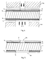
- the sensor C in FIG. 1 comprises an insulating support strip 1, made of glass or of another insulating material (even a semiconductor), crossed by a recess 2.
- this support strip can be made of a material, insulating or no, covered with an insulating layer.
- a filament 3 formed of a thin layer of an electrically conductive material and whose outer surface or skin constitutes an interface zone with the surrounding medium.
- This filament 3 has a central portion 3A and electrically conductive ends 4, by which this central portion 3A is connected to the support blade. These ends terminate in conductive pads 5 to which can be connected, for example by welding, electrical wires 6 connecting the sensor to the rest of the electrical circuit comprising it.
- This filament 3 preferably has a sinuous conformation parallel to the support blade, here in a slot which, for a given section, and a given spacing between the studs 5, gives it an increased external surface and avoids the risks of rupture by expansion. .
- Other geometric conformations are of course possible.
- the thin film filament can no longer be generally rectilinear but bent parallel to the support blade.
- the filament may have the shape of a thin blade parallel to the support blade, of course of dimensions smaller than those of the recess.
- the thin layer 3 can consist of any substance giving rise to the physico-chemical phenomena on which the measurements are based; thus this thin layer is here made of a material chosen as having electrical properties which are modified by the environment to be characterized.
- oxidizable gas of a catalytic material platinum, nickel, osmium, gold, irridium, metallic combinations, metallic oxidizable, semiconductors, sulfides ...
- This material can also be chosen as a function of its absorbent or adsorbent properties when this results in a modification of its electrical characteristics.
- FIG. 2 represents three successive layers 7, 8 and 9 respectively of conductive, insulating and catalyst material.
- the stack of layers is of the 9-8-7-8-9 type.
- Figure 3 shows another variant C ⁇ of Figure 1 in which additional end portions 10 are arranged transversely to the central portion of the 3 ⁇ filament.
- additional portions end with pads 10A. They can, in the case of a filament in a layer as in Figure 1, be used for intermediate electrical measurements or allow different assemblies making it possible to reduce the number of different sensors to manufacture and store for a given number of applications .
- these portions 10 can constitute electrical connections to the layer of catalyst which is also insulated from the conductive layer.
- the entire filament is entirely located within the size (thickness) of the substrate.
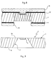
- FIGS. 4 to 9 represent, in a section plane marked A-A in FIG. 1, various stages of the method of manufacturing the sensor 1, in the example considered of a glass substrate:
- the rear mask thus obtained (layers 11 and 14) comprises a window 16A situated opposite the central portion (between the ends 4 and 5 of FIG. 1) of the window 17A of the front mask (layers 12, 13 and 15) excluding said ends, but this window 16A is larger (here wider on each side) than this central portion.
- trenches 18 and 19 are excavated by chemical attack on the glass with hydrofluoric acid through the masks consisting of superimposed layers of chromium 12, gold 13 and resin 15, engraved on the face before 1A of blade 1.
- This chemical attack is isotropic (in the thickness direction and laterally); this results in an overprint releasing the layers 12 and 13 above the inclined edges 20 of the trench thus forming an overhang 21.
- it is customary in etching processes of this type to modify the conditions for avoid over-etching here we research and use precisely this overprint. Indeed, the overhang 21 which results therefrom allows better elimination of the layers 12 and 13 at the end of manufacture.
- the resin masks 14 and 15 are eliminated, for example in acetone and then in nitric acid. A rinse with deionized water and a dust-free drying are then carried out: the structure of FIG. 6 is obtained.
- the filament 3 is produced at the bottom of the trench 18 by depositing a thin layer of chromium 23 (approximately 100 ⁇ ) on the front face 1A of the substrate including at the bottom of the trench 18 and then, by deposition over this entire thin layer 23 of a platinum layer 24 (see FIG. 7). Thin layers 23A and 24A are thus obtained in the trench dissociated from the portions 23B and 24B of gold and platinum deposited on the rest of the front face. The overall thickness of the layers 23 and 24 must therefore be less (at least slightly) than the depth of the trench 18. In the case of the sensor C 'in FIG. 2, the equivalent condition consists in saying that the overall thickness of the layers deposited is less than the depth of the trench. It is essential that the layers in the trench 18 do not come into contact with the overhangs 21.
- the side portions 24A and 23A are then removed from the excess platinum and chromium layers by chemical attack on the gold layer 13 (immersion of the substrate for at least 3 hours in a gold etching reagent which mechanically eliminates the superfluous layer of platinum, and detachment of the last traces of excess platinum in an ultrasonic tank). This operation is greatly facilitated by the overhang 21 obtained by over-etching.
- a new layer 25 of photosensitive resin of approximately 3 "m is deposited on the rear face and is then subjected to exposure through the same mask as in FIG. 4: after development, a rear mask is obtained in coincidence with the chrome mask 11 remaining on this face; in practice, the mask is then annealed at 140 ° C (for 30 min).
- the filament 3 unexpectedly remains "self-supporting" in the glass slide (see FIG. 9).
- the latter is released on the one hand from any presence of resin or polymer using a suitable chemical reagent (fuming nitric acid in general) and, on the other hand, chromium layers 11 and 12 remaining on each face of the glass slide using the chemical etching reagent for chromium.
- the advantage of the chromium layers lies on the one hand, in the improvement of the deposit of gold which could not be done directly on the glass, on the other hand, in the good performance of the mask made up of the resin layers photosensitive and chromium layers during hydrofluoric attacks on glass.
- a variant of the method consists in carrying out, according to FIGS. 5a and 6a, an operation for thickening the layer of gold. This variant thus makes it possible to deposit a greater thickness of platinum.
- the rear mask thus obtained (layer 11) comprises a window 16A situated opposite the central portion (between the ends 4 of FIG. 1) of the window 17A of the front mask (layers 12, 13) excluding of said ends, but this window 16A is larger (here wider on each side) than this central portion.
- the thickness of electrolytic gold is determined by the depth of the trenches that will be etched in the next step, ie around 1 ”m for a trench depth of 10 to 15” m.
- a uniform layer of photosensitive protective resin 11bis is deposited on the rear face.
- the trench 18 is excavated by chemical attack on the glass with hydrofluoric acid through the mask consisting of superimposed layers of chromium 12, gold 13 and 13bis, etched on the front face 1A of blade 1.
- This chemical attack is isotropic (in the thickness direction and laterally); this results in an over-etching releasing the layers 12, 13 and 13a above the inclined edges 20 of the trench thus forming an overhang 21.
- it is customary in etching processes of this type to modify their conditions to avoid over-etching here we research and use precisely this over-etching. Indeed, the overhang 21 which results therefrom allows better elimination of the layers 12 and 13 at the end of manufacture.
- the resin mask 11bis is eliminated for example in acetone then in nitric acid. Then rinse with deionized water and dry off dust: the structure of the figure 6.
- glass Apart from glass, it is possible to use other substrates: silicon, alumina, silica and in particular quartz which offers good temperature resistance and selective resistance to chemical attack.
- Such a sensor is suitable for various applications.
- the filament 3 is used to locally heat and ionize the gaseous medium and one or more ion receiving electrodes (interface area) are formed by one or more thin conductive layers deposited on the substrate near the recess 2: it may be the chromium layers 11 and 12 which are left to remain for this purpose.
Abstract
Description
La présente invention concerne un capteur du type à filament pour la détermination d'une caractéristique statique ou dynamique d'un milieu gazeux environnant, tel que l'air par exemple, un procédé pour sa fabrication, et des applications de ce capteur, principalement dans la détection de gaz oxydables mais aussi en chromatographie gazeuse (détection de gaz ionisables) ou encore dans la mesure de débits fluides.The present invention relates to a filament type sensor for determining a static or dynamic characteristic of a surrounding gaseous medium, such as air for example, a method for its manufacture, and applications of this sensor, mainly in the detection of oxidizable gases but also in gas chromatography (detection of ionizable gases) or even in the measurement of fluid flow rates.
Un tel capteur du type à filament peut se définir comme étant un capteur comportant un élément résistif au sein d'un filament destiné à échanger de la chaleur avec l'environnement, ainsi qu'une zone d'interface adaptée à réagir avec ce milieu selon un processus physico-chimique (au sens le plus large du terme : catalyse de combustion, adsorption, ionisation, simple échange thermique) influant, en fonction de la caractéristique du milieu à déterminer (concentration, débit ...), sur une caractéristique électrique de cette zone d'interface (température ou résistance, tension, intensité..). Cette zone d'interface peut aussi bien être la portion externe de l'élément résistif, qu'une couche catalytique chauffée par conduction, une électrode distincte.Such a filament type sensor can be defined as being a sensor comprising a resistive element within a filament intended to exchange heat with the environment, as well as an interface zone adapted to react with this medium according to a physico-chemical process (in the broadest sense of the term: combustion catalysis, adsorption, ionization, simple heat exchange) influencing, depending on the characteristic of the medium to be determined (concentration, flow ...), on an electrical characteristic of this interface zone (temperature or resistance, voltage, intensity, etc.). This interface zone may as well be the external portion of the resistive element, as a catalytic layer heated by conduction, a separate electrode.
Certains de ces capteurs sont ainsi fondés sur une mesure de chaleur échangée (détection de gaz combustible, debitmètre ...) et on peut les qualifier de capteurs calorimétriques; on peut aussi recenser divers capteurs du type à filament ayant en commun de mesurer une concentration, en étant fondés sur des phénomènes divers (mesure de chaleur échangée dans le cas de la détection de gaz combustible ou oxydable par exemple, mesure de quantités d'ions recueillis par une électrode dans la chromatographie gazeuse par exemple ....). Les capteurs du type à filament regroupent donc des capteurs très divers, tant en ce qui concerne le phénomène physico-chimique sur lequel ils sont fondés qu'en ce qui concerne la nature de la grandeur à mesurer.Some of these sensors are thus based on a measurement of heat exchanged (detection of combustible gas, flow meter, etc.) and can be qualified as calorimetric sensors; one can also identify various sensors of the filament type having in common to measure a concentration, being based on various phenomena (measurement of heat exchanged in the case of the detection of combustible or oxidizable gas for example, measurement of quantities of ions collected by an electrode in chromatography gas for example ....). Filament type sensors therefore group together very diverse sensors, both with regard to the physico-chemical phenomenon on which they are based and with regard to the nature of the quantity to be measured.
C'est pourquoi, si la suite de l'exposé se réfère principalement à la détection d'un gaz oxydable dans un milieu gazeux tel que l'air, dans le domaine par exemple de l'explosimétrie, il s'agit d'une application préférée mais non limitative de l'invention.This is why, if the rest of the presentation refers mainly to the detection of an oxidizable gas in a gaseous medium such as air, in the field for example of explosimetry, it is a question of preferred but not limiting application of the invention.
De manière connue en soi, la détection d'un gaz oxydable dans l'air est assurée par un filament, généralement de platine, chauffé par effet JOULE, c'est à dire par passage d'un courant électrique. Le gaz oxydable contenu dans l'air environnant s'oxyde par catalyse au contact du filament, d'où un échauffement supplémentaire de ce dernier. La variation de température qui en résulte provoque une variation de la résistance du filament, dont la mesure directe ou indirecte permet d'avoir accès à la concentration dudit gaz oxydable dans l'air. Ces détecteurs à base de filament sont faits de manière assez artisanale, comportant une partie de fabrication manuelle. Ils souffrent donc d'un manque de reproductibilité et d'un prix de revient élevé. Leur faible résistance électrique, et leur faible rapport surface/volume, obligent à travailler à haute température (1000°C environ).In a manner known per se, the detection of an oxidizable gas in the air is ensured by a filament, generally of platinum, heated by JOULE effect, that is to say by passage of an electric current. The oxidizable gas contained in the surrounding air oxidizes by catalysis on contact with the filament, resulting in additional heating of the latter. The resulting temperature variation causes a variation in the resistance of the filament, the direct or indirect measurement of which gives access to the concentration of said oxidizable gas in the air. These filament-based detectors are made in a fairly traditional way, including a part of manual manufacture. They therefore suffer from a lack of reproducibility and a high cost price. Their low electrical resistance, and their low surface / volume ratio, make it necessary to work at high temperature (approximately 1000 ° C).
D'autres détecteurs de gaz oxydable sont constitués à partir de perles catalytiques; ils sont formés d'un détecteur métallique (par exemple en platine) enrobé d'alumine dopée à l'aide d'un catalyseur, ayant l'apparence d'une petite perle. Le vieillissement de ces détecteurs est moins rapide, car la température de combustion qui leur est associée est plus faible. Cependant, ces perles souffrent d'une dérive importante de la sensibilité, d'une stabilité moins grande et d'un temps de réponse plus long que les filaments.Other oxidizable gas detectors are made from catalytic beads; they are formed by a metal detector (for example made of platinum) coated with alumina doped with the aid of a catalyst, having the appearance of a small pearl. The aging of these detectors is slower because the combustion temperature associated with them is lower. However, these pearls suffer from a significant drift in sensitivity, less stability and a longer response time than the filaments.
Un troisième type de détecteur de gaz oxydable a été réalisé à partir d'oxydes métalliques semiconducteurs dopés avec un catalyseur. Ces détecteurs sont formés d'un filament métallique de chauffage, chauffant un manchon isolant, en alumine par exemple, sur lequel est déposée une couche de matériau semiconducteur, dont on mesure les variations de résistances. Ces détecteurs sont sensibles à tout gaz adsorbable à la surface du semiconducteur. Mais ils ont un temps de réponse assez long et une consommation électrique importante ; de plus l'influence de l'humidité n'y est pas compensée.A third type of oxidizable gas detector has been produced from semiconductor metal oxides doped with a catalyst. These detectors are formed of a metallic heating filament, heating an insulating sleeve, made of alumina for example, on which is deposited a layer of semiconductor material, the variations of resistances of which are measured. These detectors are sensitive to any gas adsorbable on the surface of the semiconductor. But they have a fairly long response time and a significant electrical consumption; moreover the influence of humidity is not compensated for there.
Une présentation brève et générale des capteurs à filaments ou à perles catalytiques est donnée dans le préambule du document WO-90/12313 (à prendre en considération selon l'article 54(3) CBE en ce qui concerne ses enseignements).A brief and general presentation of the filament or catalytic bead sensors is given in the preamble to document WO-90/12313 (to be taken into account according to Article 54 (3) EPC with regard to its teachings).
Un autre type de dispositif détecteur est décrit dans le document DE-A-3.743.398 : le dispositif détecteur comporte un substrat semiconducteur dans lequel est ménagée une ouverture ; ce substrat se prolongeant dans cette ouverture par deux bras recouverts d'une couche de passivation ; ces bras portent par leurs extrémités un élément semiconducteur de faible étendue, sensible à la température, en contact avec une couche de matériau catalytique. Il ne s'agit pas d'un détecteur à filament.Another type of detector device is described in document DE-A-3,743,398: the detector device comprises a semiconductor substrate in which an opening is formed; this substrate extending into this opening by two arms covered with a passivation layer; these arms carry by their ends a semiconductor element of small extent, sensitive to temperature, in contact with a layer of catalytic material. It is not a filament detector.
Quant au document GB-A-2.158.586, il décrit un dispositif pour la détection de la combustion catalytique du méthane. Une résistance de chauffage en couche mince ou épaisse est déposée sur un substrat muni sur son autre face d'un élément sensible à la température. Une couche catalytique est déposée sur la résistance de chauffage et éventuellement sur le substrat. Il peut y avoir des pertes thermiques par conduction au sein du substrat plan.As for document GB-A-2,158,586, it describes a device for detecting the catalytic combustion of methane. A thin or thick layer heating resistance is deposited on a substrate provided on its other face with a temperature-sensitive element. A catalytic layer is deposited on the heating resistor and possibly on the substrate. There may be heat losses by conduction within the planar substrate.
Le document EP-A-0.377.792, à prendre en considération selon l'article 54(3)CBE pour AT, CH, DE, FR, GB, IT, NL, décrit un capteur pour la détection de gaz comprenant une plaque de support comportant une fenêtre, une couche isolante couvrant la plaque de support et constituant une membrane libre au-dessus de la fenêtre. Sur cette couche isolante sont disposées des résistances en couche mince, une couche de protection et une couche catalytique recouvrant la zone adaptée à être chauffée par les résistances. Il y a des risques de pertes thermiques par conduction transversalement aux résistances.Document EP-A-0.377.792, to be taken into account according to article 54 (3) EPC for AT, CH, DE, FR, GB, IT, NL, describes a sensor for detecting gas comprising a support plate comprising a window, an insulating layer covering the support plate and constituting a free membrane above the window. On this insulating layer are arranged resistors in a thin layer, a protective layer and a catalytic layer covering the zone suitable for being heated by the resistors. There are risks of thermal losses by conduction transverse to the resistors.
L'invention vise à pallier les inconvénients précités en améliorant la reproductibilité et en réduisant les pertes thermiques du filament par conduction, notamment transversalement au filament, tout en abaissant les coûts de fabrication.The invention aims to overcome the aforementioned drawbacks by improving the reproducibility and reducing the thermal losses of the filament by conduction, in particular transversely to the filament, while lowering the manufacturing costs.
De manière très générale, elle propose à cet effet un capteur à filament pour la détermination d'une caractéristique statique ou dynamique d'un milieu environnant, comportant un élément résistif destiné à être chauffé par effet JOULE dans ce milieu, et une zone d'interface adaptée à réagir avec ce milieu selon un processus physico-chimique influant, en fonction de la caractéristique à déterminer, sur une caractéristique électrique de cette zone d'interface, ce capteur comportant une lame de support traversée par au moins un évidement et au moins un filament incluant cet élément résistif, constitué d'une ou plusieurs couche(s) mince(s) et comportant une portion centrale s'étendant librement dans l'évidement et au moins deux portions d'extrémité par lesquelles cette portion centrale est reliée à la lame de support, grâce à quoi ce filament est autoporté.In a very general way, it proposes for this purpose a filament sensor for the determination of a static or dynamic characteristic of a surrounding medium, comprising a resistive element intended to be heated by JOULE effect in this medium, and a zone of interface adapted to react with this medium according to a physicochemical process influencing, as a function of the characteristic to be determined, on an electrical characteristic of this interface zone, this sensor comprising a support blade crossed by at least one recess and at least a filament including this resistive element, consisting of one or more thin layer (s) and comprising a central portion extending freely in the recess and at least two end portions by which this central portion is connected to the support blade, thanks to which this filament is self-supporting.
En d'autres termes l'invention propose un filament réalisé à l'aide des technologies de la microélectronique, construit de telle façon qu'il "s'autosupporte", c'est-à-dire que ses seuls éléments de liaison avec le support sont des couches minces : le filament est ainsi constitué d'une ou plusieurs couches minces "en l'air" ce qui réduit considérablement les pertes thermiques par conduction.In other words, the invention proposes a filament produced using microelectronics technologies, constructed in such a way that it "self-supports", that is to say that its only elements of connection with the support are thin layers: the filament is like this consisting of one or more thin layers "in the air" which considerably reduces thermal losses by conduction.
L'invention résulte de la constatation qu'il était possible, grâce à cette technologie des couches minces, de réaliser un filament présentant une résistance mécanique et une tenue aux chocs thermiques suffisantes pour qu'il puisse s'autoporter.The invention results from the observation that it was possible, thanks to this technology of thin layers, to produce a filament having sufficient mechanical strength and resistance to thermal shock so that it can be self-supporting.
Les demanderesses ont en effet constaté de manière surprenante que, malgré la finesse du filament qui lui confère la résistance électrique voulue, celui-ci est à la fois suffisamment sensible pour permettre la réaction physico-chimique à l'origine de la mesure et suffisamment résistant pour ne pas s'user prématurément en contact avec le milieu environnant.The applicants have in fact surprisingly found that, despite the fineness of the filament which gives it the desired electrical resistance, it is both sufficiently sensitive to allow the physicochemical reaction at the origin of the measurement and sufficiently resistant so as not to wear out prematurely in contact with the surrounding environment.
Selon des dispositions préférées de l'invention :
- le filament est formé d'une couche en matériau métallique catalytique dont la surface extérieure constitue ladite zone d'interface;
- le filament, au moins dans sa portion centrale, est formé d'un empilement d'au moins trois couches minces, dont une couche en matériau conducteur, se prolongeant jusqu'aux extrémités du filament, une couche en matériau catalyseur formant la zone d'interface et une couche intermédiaire en matériau électriquement isolant,
- l'élément résistif du filament est une couche d'un métal noble, notamment platine, or, palladium ou en une combinaison de métaux nobles,
- le filament a une conformation sinueuse, par exemple en créneau,
- la portion centrale du filament est reliée au substrat par un nombre de portions d'extrémité supérieur à deux,
- le substrat est choisi dans le groupe de matériaux constitué par le verre, le silicium, l'alumine, la silice, le quartz et les polymères,
- la zone d'interface est une couche mince déposée au moins sur l'une des faces du substrat à proximité de l'évidement.
- the filament is formed of a layer of catalytic metallic material, the outer surface of which constitutes said interface zone;
- the filament, at least in its central portion, is formed of a stack of at least three thin layers, including a layer of conductive material, extending to the ends of the filament, a layer of catalyst material forming the zone of interface and an intermediate layer of electrically insulating material,
- the resistive element of the filament is a layer of a noble metal, in particular platinum, gold, palladium or in a combination of noble metals,
- the filament has a sinuous conformation, for example in niche,
- the central portion of the filament is connected to the substrate by a number of end portions greater than two,
- the substrate is chosen from the group of materials consisting of glass, silicon, alumina, silica, quartz and polymers,
- the interface zone is a thin layer deposited at least on one of the faces of the substrate near the recess.
L'invention propose également un procédé de préparation de filament faisant appel à des techniques de microélectronique, adapté à la fabrication du capteur précité et caractérisé en ce qu'il comporte les étapes suivantes :
- dépôt sur la surface des faces respectivement avant et arrière d'un substrat en forme de lame, d'une part, d'un masque avant en couche(s) mince(s) comportant un fenêtre avant dont la forme correspond à la forme du filament à fabriquer et comporte une portion centrale prolongée par des portions d'extrémité, et d'autre part, d'un masque arrière en couche(s) mince(s) comportant une fenêtre arrière située en regard de la portion centrale de la fenêtre à l'exclusion desdites extrémités, mais plus grande que cette portion centrale,
- creusement d'une tranchée dans le substrat par attaque de la face avant de celui-ci à travers le masque avant,
- dépôt au fond de cette tranchée d'une ou plusieurs couche(s) mince(s) destinée(s) à constituer le filament et dont l'une au moins est en matériau électriquement conducteur, et
- élimination du substrat sur toute son épaisseur par attaque à travers le masque arrière.
- deposition on the surface of the front and rear faces respectively of a blade-shaped substrate, on the one hand, of a front mask in thin layer (s) comprising a front window whose shape corresponds to the shape of the filament to be manufactured and comprises a central portion extended by end portions, and on the other hand, a rear mask in thin layer (s) comprising a rear window located opposite the central portion of the window excluding said ends, but larger than this central portion,
- digging a trench in the substrate by attacking the front face of the latter through the front mask,
- deposition at the bottom of this trench of one or more thin layer (s) intended to constitute the filament and at least one of which is made of electrically conductive material, and
- elimination of the substrate over its entire thickness by attack through the rear mask.
Selon des dispositions préférées :
- avant attaque du substrat pour son élimination sur toute son épaisseur à travers le masque arrière, on procède au dépôt d'une couche de protection sur la face avant et dans la tranchée et, après cette attaque du substrat, à l'élimination de cette couche de protection,
- la couche de protection de la face avant est une résine polymère,
- le masque avant comporte une couche intermédiaire recouverte d'une couche de résine, le dépôt de la (ou des) couche(s) mince(s) du filament étant obtenu, après élimination de la couche de résine, par dépôt d'une ou plusieurs couche(s) minces(s) dans la tranchée et autour de celle-ci puis élimination de la (ou des) couche(s) minces(s) déposée(s) en dehors de la tranchée par attaque de la couche intermédiaire.
- before attacking the substrate for its elimination over its entire thickness through the rear mask, a protective layer is deposited on the front face and in the trench and, after this attack on the substrate, the elimination of this layer protection,
- the protective layer of the front face is a polymer resin,
- the front mask comprises an intermediate layer covered with a resin layer, the deposit of the thin layer (s) of the filament being obtained, after elimination of the resin layer, by depositing one or more several thin layer (s) in and around the trench then elimination of the thin layer (s) deposited outside the trench by attacking the intermediate layer.
Les principaux avantages qui découlent de l'invention sont, par rapport à tous les éléments détecteurs cités précédemment, une consommation électrique très faible, et un temps de réponse également très faible.The main advantages which flow from the invention are, compared with all the detector elements mentioned above, a very low electrical consumption, and a response time also very low.
De réalisation automatisable et collective, le capteur peut être fabriqué d'une façon reproductible et en grande quantité à coût faible.Automated and collective, the sensor can be manufactured in a reproducible manner and in large quantities at low cost.
Sa résistance, ajustable en fonction de sa forme géométrique, permet une température de fonctionnement plus basse que les capteurs traditionnels à filament, ce qui entraîne une bonne résolution de la mesure, et un vieillissement moins rapide. Par suite de sa réalisation originale et grâce à la masse très faible qui en résulte, il est peu sensible aux chocs.Its resistance, adjustable according to its geometric shape, allows a lower operating temperature than traditional filament sensors, which results in good resolution of the measurement, and slower aging. Due to its original construction and thanks to the very low mass that results, it is not very sensitive to shocks.
Du fait de son inertie thermique très faible, il peut permettre également d'éffectuer des mesures à des températures différentes et à des intervalles de temps très courts.Due to its very low thermal inertia, it can also allow measurements to be made at different temperatures and at very short time intervals.
L'invention porte également sur l'application d'un tel capteur, principalement à la détection de gaz oxydable, tel que le méthane, ou CO, mais encore à la chromatographie gazeuse (détection de gaz ionisables) ou à la mesure de débits gazeux par calorimétrie.The invention also relates to the application of such a sensor, mainly to the detection of oxidizable gas, such as methane, or CO, but also to gas chromatography (detection of ionizable gases) or to the measurement of gas flow rates. by calorimetry.
Des objets, caractéristiques de l'invention ressortent de la description des dessins sur lesquels :
- la figure 1 est une vue en perspective d'un capteur selon l'invention,
- la figure 2 est une vue partielle en coupe longitudinale d'un autre capteur dans le sens de l'épaisseur,
- la figure 3 est une variante de la figure 1, et
- les figures 4 à 9 sont des vues en coupe du capteur de la figure 1 à divers stades de sa fabrication à partir d'un substrat selon le procédé de l'invention.
- FIG. 1 is a perspective view of a sensor according to the invention,
- Figure 2 is a partial sectional view longitudinal of another sensor in the thickness direction,
- FIG. 3 is a variant of FIG. 1, and
- Figures 4 to 9 are sectional views of the sensor of Figure 1 at various stages of its manufacture from a substrate according to the method of the invention.
Le capteur C de la figure 1 comporte une lame isolante de support 1, en verre ou en un autre matériau isolant (voire semi-conducteur), traversée par un évidement 2. En variante cette lame de support peut être en un matériau, isolant ou non, recouvert d'une couche isolante.The sensor C in FIG. 1 comprises an insulating
En travers de l'évidement est disposé un filament 3 formé d'une couche mince en un matériau électriquement conducteur et dont la surface extérieure ou peau constitue une zone d'interface avec le milieu environnant.Across the recess is disposed a
Ce filament 3 comporte une portion centrale 3A et des extrémités 4 électriquement conductrices, par lesquelles cette portion centrale 3A est reliée à la lame de support. Ces extrémités se terminent par des plots conducteurs 5 auxquels peuvent être connectés, par exemple par soudure, des fils électriques 6 reliant le capteur au reste du circuit électrique le comportant.This
Ce filament 3 a de préférence une conformation sinueuse parallèlement à la lame de support, ici en créneau ce qui, pour une section donnée, et un écartement donné entre les plots 5, lui confère une surface extérieure accrue et évite les risques de rupture par dilatation. D'autres conformations géométriques sont bien sûr possibles. Il est à préciser à ce propos que le filament en couche mince peut être non plus globalement rectiligne mais coudé parallèlement à la lame de support. Par ailleurs, le filament peut avoir la forme d'une fine lame parallèle à la lame de support, de dimensions bien sûr inférieures à celles de l'évidement.This
La couche mince 3 peut être constituée par toute substance donnant lieu aux phénomènes physico-chimiques sur lesquels sont fondées les mesures; ainsi cette couche mince est ici réalisée en un matériau choisi comme ayant des propriétés électriques qui sont modifiées par l'environnement à caractériser.The
Il peut en particulier s'agir pour la mesure de gaz oxydable d'un matériau catalytique : platine, nickel, osmium, or, irridium, combinaisons métalliques, oxydables métalliques, semi-conducteurs, sulfures ...It can in particular be for the measurement of oxidizable gas of a catalytic material: platinum, nickel, osmium, gold, irridium, metallic combinations, metallic oxidizable, semiconductors, sulfides ...
Ce matériau peut être également choisi en fonction de ses propriétés absorbantes ou adsorbantes dès lors qu'il en résulte une modification de ses caractéristiques électriques.This material can also be chosen as a function of its absorbent or adsorbent properties when this results in a modification of its electrical characteristics.
La figure 2 (où les éléments similaires à ceux de la figure 1 ont les mêmes signes de référence affectés de l'indice "prime") représente un autre capteur C′ dont le filament 3′ est constitué, non plus d'une seule couche mince, mais d'un empilement de couches minces en matériau conducteur, isolant ou catalyseur. La succession de ces couches est telle que :
- chaque couche en matériau catalyseur est située au-dessus ou en-dessous de l'empilement,
- chaque couche électriquement conductrice est reliée électriquement aux plots 5, et
- une couche isolante est prévue entre ces couches en matériau conducteur ou catalyseur.
- each layer of catalyst material is located above or below the stack,
- each electrically conductive layer is electrically connected to the
pads 5, and - an insulating layer is provided between these layers of conductive or catalyst material.
Plus précisément, cette figure 2 représente trois couches successives 7, 8 et 9 respectivement en matériau conducteur, isolant et catalyseur. En variante non représentée l'empilement des couches est de type 9-8-7-8-9.More precisely, this FIG. 2 represents three
La figure 3 (où les éléments similaires à ceux de la figure 1 ont les mêmes signes de référence affectés de l'indice "seconde") représente une autre variante C˝ de la figure 1 dans laquelle des portions d'extrémité additionnelles 10 sont disposées transversalement à la portion centrale du filament 3˝. Ces portions additionnelles se terminent par des plots 10A. Ils peuvent, dans le cas d'un filament en une couche comme dans la figure 1, servir à des mesures électriques intermédiaires ou permettre des montages différents rendant possible de réduire le nombre de capteurs différents à fabriquer et stocker pour un nombre donné d'applications. Dans le cas d'un filament multicouche comme dans la figure 2, ces portions 10 peuvent constituer des liaisons électriques à la couche de catalyseur par ailleurs isolée par rapport à la couche conductrice.Figure 3 (where elements similar to those of Figure 1 have the same reference signs assigned the index "second") shows another variant C˝ of Figure 1 in which
On appréciera que dans chacun des exemples précités, l'ensemble du filament est entièrement situé dans l'encombrement (l'épaisseur) du substrat.It will be appreciated that in each of the above examples, the entire filament is entirely located within the size (thickness) of the substrate.
Les figures 4 à 9 représentent, dans un plan de coupe repéré A-A sur la figure 1, diverses étapes du procédé de fabrication du capteur 1, dans l'exemple considéré d'un substrat en verre :FIGS. 4 to 9 represent, in a section plane marked A-A in FIG. 1, various stages of the method of manufacturing the
Une première phase consiste à préparer le substrat 1 par :
- nettoyage du substrat 1 à l'acide nitrique ou sulfochromique par exemple puis rinçage à l'eau désionisée,
- séchage hors poussière.
- cleaning of the
substrate 1 with nitric or sulfochromic acid for example then rinsing with deionized water, - dust-free drying.
En une deuxième phase, on prépare des masques sur chacune des faces avant 1A et arrière 1B du substrat, avec les étapes suivantes (voir la figure 4) :
- une couche mince de
chrome 11 de 1000 à 2000 Å est déposée sur la face arrière; sur l'autre face (face avant), une couche dechrome 12 de quelques Å à 1000 Å puis une couched'or 13 de 1000 Å environ sont déposées. Les étapes peuvent être différées l'une par rapport à l'autre mais sont de préférence simultanées. - une couche de résine photosensible 14, 15 est déposée sur chaque face du substrat,
- on positionne des masques d'insolation 14A et 15A en vis-à-vis de part et d'autre du substrat et des couches précitées, on procède à l'insolation des
couches 14 et 15 au travers des masques 14A et 15A, et on développe les zones ainsi insolées : on obtient ainsi des masques de résine 16et 17. Les deux dernières étapes sont tout à fait classiques en soi. - on grave les couches métalliques au travers des masques 16
et 17,- . gravure de la couche de
chrome 11 sur la face arrière, - . gravure de la couche
d'or 13 sur la face avant, - . gravure de la couche de
chrome 12 en face avant.
- . gravure de la couche de
- nouveau rinçage à l'eau désionisée; on obtient ainsi la structure de la figure 5.
- a thin layer of
chromium 11 of 1000 to 2000 Å is deposited on the rear face; on the other face (front face), a layer ofchromium 12 of a few Å to 1000 Å and then a layer ofgold 13 of around 1000 Å are deposited. The steps can be differed from each other but are preferably simultaneous. - a layer of
photosensitive resin - exposure masks 14A and 15A are positioned opposite each other of the substrate and the abovementioned layers, exposure of the
layers masks 14A and 15A, and develops the areas thus exposed: one thus obtains masks ofresin - the metal layers are etched through
masks - . etching of the
chromium layer 11 on the rear face, - . engraving of the
gold layer 13 on the front face, - . etching of the
chrome layer 12 on the front face.
- . etching of the
- new rinse with deionized water; the structure of FIG. 5 is thus obtained.
On appréciera que le masque arrière ainsi obtenu (couches 11 et 14) comporte une fenêtre 16A située en regard de la portion centrale (entre les extrémités 4 et 5 de la figure 1) de la fenêtre 17A du masque avant (couches 12, 13 et 15) à l'exclusion desdites extrémités, mais cette fenêtre 16A est plus grande (ici plus large de chaque côté) que cette portion centrale.It will be appreciated that the rear mask thus obtained (
Dans une troisième phase, on procède au creusement de tranchées 18 et 19 par attaque chimique du verre avec de l'acide fluorhydrique à travers les masques constitués des couches superposées de chrome 12, d'or 13 et de résine 15, gravées sur la face avant 1A de la lame 1. Cette attaque chimique est isotrope (dans le sens de l'épaisseur et latéralement); il en résulte une surgravure dégageant les couches 12 et 13 au-dessus des bords inclinés 20 de la tranchée formant ainsi un surplomb 21. Alors qu'il est d'usage dans les procédés de gravure de ce type d'en modifier les conditions pour éviter la surgravure, ici on recherche et utilise précisément cette surgravure. En effet, le surplomb 21 qui en résulte permet une meilleure élimination des couches 12 et 13 en fin de fabrication.In a third phase,
Les masques de résine 14 et 15 sont éliminés par exemple dans l'acétone puis dans l'acide nitrique. On effectue ensuite un rinçage à l'eau désionisée et un séchage hors poussière : on obtient la structure de la figure 6.The resin masks 14 and 15 are eliminated, for example in acetone and then in nitric acid. A rinse with deionized water and a dust-free drying are then carried out: the structure of FIG. 6 is obtained.
Dans une quatrième étape, on élabore le filament 3 au fond de la tranchée 18 par dépôt d'une fine couche de chrome 23 (100 Å environ) sur la face avant 1A du substrat y compris au fond de la tranchée 18 puis, par dépôt sur toute cette couche mince 23 d'une couche de platine 24 (voir figure 7). On obtient ainsi dans la tranchée des couches minces 23A et 24A dissociées des portions 23B et 24B d'or et de platine déposées sur le reste de la face avant. L'épaisseur globale des couches 23 et 24 doit donc être inférieure (au moins légèrement) à la profondeur de la tranchée 18. Dans le cas du capteur C' de la figure 2, la condition équivalente consiste à dire que l'épaisseur globale des couches déposées est inférieure à la profondeur de la tranchée. Il est essentiel que les couches dans la tranchée 18 ne viennent pas au contact des surplombs 21.In a fourth step, the
On procède ensuite à l'élimination des portions latérales 24A et 23A des couches de platine et de chrome en excès par attaque chimique de la couche d'or 13 (immersion du substrat pendant au moins 3 heures dans un réactif de gravure de l'or ce qui élimine mécaniquement la couche superflue de platine, et décollement des dernières traces de platine en excès dans un bac à ultra-sons). Cette opération est grandement facilitée par le surplomb 21 obtenu par surgravure.The
Après rinçage à l'eau désionisée et séchage, une nouvelle couche 25 en résine photosensible de 3»m environ est déposée sur la face arrière puis est soumise à une insolation à travers le même masque qu'à la figure 4 : après développement, on obtient un masque arrière en coïncidence avec le masque en chrome 11 resté sur cette face; en pratique, on procède ensuite au recuit du masque à 140°C (pendant 30 mn).After rinsing with deionized water and drying, a
Dans une dernière phase, on creuse le substrat sur toute son épaisseur par attaque au travers du masque arrière selon les étapes suivantes :
- dépôt d'une couche de
protection 26 sur laface avant 1A revêtue de la couche dechrome 12. Cette couche de protection remplit la cuvette 18 et en y adhérant recouvre le filament au fond de cette dernière. Cette couche de protection peut être constituée de tout matériau résistant à l'acide fluorhydrique et pouvant facilement être mis en solution à l'aide d'un solvant du commerce. On utilise de manière préférentielle une résine polymère du type APIEZON-W de ZIVY, - attaque chimique sous ultra-sons du verre 1 portant le filament à travers le masque 25 déposé sur la face arrière 1B et constitué de la couche de
chrome 11 et de la couche de résine photosensible 25 gravées.
- depositing a
protective layer 26 on thefront face 1A coated with thechromium layer 12. This protective layer fills thebowl 18 and by adhering to it covers the filament at the bottom of the latter. This protective layer may consist of any material resistant to hydrofluoric acid and which can easily be dissolved using a commercial solvent. A polymer resin of the APIEZON-W type from ZIVY is preferably used, - chemical attack under ultrasound of the
glass 1 carrying the filament through themask 25 deposited on the rear face 1B and consisting of thechromium layer 11 and thephotosensitive resin layer 25 etched.
Après élimination du verre et de la couche de protection 26 à l'aide d'un solvant du commerce approprié; par exemple du perchloréthylène, le filament 3 reste d'une manière inattendue "autoporté" dans la lame de verre (voir figure 9). Cette dernière est dégagée d'une part de toute présence de résine ou de polymère à l'aide d'un réactif chimique adapté (acide nitrique fumant en général) et, d'autre part, des couches de chrome 11 et 12 subsistant sur chaque face de la lame de verre à l'aide du réactif de gravure chimique du chrome.After removing the glass and the
L'inclinaison des flancs de l'évidement 2 de la figure 9 provient du caractère isotrope de l'attaque fluorhydrique. Dans le cas d'un substrat et d'un acide d'attaque conduisant à une attaque anisotrope, on obtiendrait des flancs verticaux comme cela est représenté aux figures 7 et 8.The inclination of the sides of the
A titre d'exemple les réactifs de gravure chimique utilisés sont :
- . chrome :
- 1) Cr-ETCH de SOPRELEC (EVRY)
- 2) 50g/l de KMnO4 + 50g/l de KOH + eau désionisée (1l),
- . or : 25g/l de I₂ = 60g/l de KI + 1 litre d'eau désionisée,
- . verre : HF dilué de 40% à 20% (suivant la vitesse de gravure désirée).
- . chrome:
- 1) Cr-ETCH from SOPRELEC (EVRY)
- 2) 50g / l of KMnO4 + 50g / l of KOH + deionized water (1l),
- . gold: 25g / l of I₂ = 60g / l of KI + 1 liter of deionized water,
- . glass: HF diluted from 40% to 20% (depending on the desired etching speed).
Des exemples d'épaisseurs pour des lames de verre de 150 »m d'épaisseur sont :
- . chrome N° 11 : 500 Å à 1000 Å
- . chrome N°s 12 et 23 : 50 Å à 500 Å
- . or N° 13 : 1500 Å à 2500 Å
- . platine : 0,5 »m à 9 »m
- . apiézon W : minimum 100 »m
- . résine photosensible 1350-H de SHIPPLEY : 1 à 3 »m
- . longueur de l'évidement : 2 mm.
- . chrome N ° 11: 500 Å to 1000 Å
- . chrome N ° s 12 and 23: 50 Å to 500 Å
- . or N ° 13: 1500 Å to 2500 Å
- . platinum: 0.5 "m to 9" m
- . apiézon W: minimum 100 ”m
- . SHIPPLEY 1350-H photosensitive resin: 1 to 3 ”m
- . length of the recess: 2 mm.
L'intérêt des couches de chrome réside d'une part, dans l'amélioration du dépôt d'or qui ne pourrait pas se faire directement sur le verre, d'autre part, dans la bonne tenue du masque constitué pas les couches de résine photosensible et les couches de chrome lors des attaques fluorhydriques du verre.The advantage of the chromium layers lies on the one hand, in the improvement of the deposit of gold which could not be done directly on the glass, on the other hand, in the good performance of the mask made up of the resin layers photosensitive and chromium layers during hydrofluoric attacks on glass.
Une variante du procédé consiste à réaliser selon les figures 5bis et 6bis une opération d'épaississement de la couche d'or. Cette variante permet ainsi de déposer une épaisseur de platine plus importante.A variant of the method consists in carrying out, according to FIGS. 5a and 6a, an operation for thickening the layer of gold. This variant thus makes it possible to deposit a greater thickness of platinum.
Les deuxième et troisième phases du procédé sont modifiées ainsi :The second and third phases of the process are modified as follows:
A l'issue des gravures métalliques au travers des masques 16 et 17 on procède à :
- un décapage des couches de résines 14 et 15 à l'acétone et à l'acide nitrique
- puis à un nouveau rinçage à l'eau désionisée.
- pickling of resin layers 14 and 15 with acetone and nitric acid
- then a further rinse with deionized water.
On appréciera que le masque arrière ainsi obtenu (couche 11) comporte une fenêtre 16A située en regard de la portion centrale (entre les extrémités 4 de la figure 1) de la fenêtre 17A du masque avant (couches 12, 13) à l'exclusion desdites extrémités, mais cette fenêtre 16A est plus grande (ici plus large de chaque côté) que cette portion centrale.It will be appreciated that the rear mask thus obtained (layer 11) comprises a
On procède ensuite à une opération d'épaississement de la couche d'or 13 (figure 5bis) par dépôt électrolytique d'or (couche 13bis) suivie d'un rinçage à l'eau désionisée.Then a thickening operation of the gold layer 13 (FIG. 5bis) is carried out by electrolytic deposition of gold (layer 13bis) followed by rinsing with deionized water.
L'épaisseur d'or électrolytique est déterminée par la profondeur des tranchées que l'on va graver dans l'étape suivante soit environ 1»m pour une profondeur de tranchée de 10 à 15 »m. On dépose sur la face arrière une couche uniforme de résine photosensible de protection 11bis.The thickness of electrolytic gold is determined by the depth of the trenches that will be etched in the next step, ie around 1 ”m for a trench depth of 10 to 15” m. A uniform layer of photosensitive protective resin 11bis is deposited on the rear face.
Dans la troisième phase, on procède au creusement de la tranchée 18 par attaque chimique du verre avec de l'acide fluorhydrique à travers le masque constitué des couches superposées de chrome 12, d'or 13 et 13bis, gravées sur la face avant 1A de la lame 1. Cette attaque chimique est isotrope (dans le sens de l'épaisseur et latéralement); il en résulte une surgravure dégageant les couches 12, 13 et 13bis au-dessus des bords inclinés 20 de la tranchée formant ainsi un surplomb 21. Alors qu'il est d'usage dans les procédés de gravure de ce type d'en modifier les conditions pour éviter la surgravure, ici on recherche et utilise précisément cette surgravure. En effet, le surplomb 21 qui en résulte permet une meilleure élimination des couches 12 et 13 en fin de fabrication.In the third phase, the
Le masque de résine 11bis est éliminé par exemple dans l'acétone puis dans l'acide nitrique. On effectue ensuite un rinçage à l'eau désionisée et un séchage hors poussière : on obtient la structure de la figure 6.The resin mask 11bis is eliminated for example in acetone then in nitric acid. Then rinse with deionized water and dry off dust: the structure of the figure 6.
Les phases ultérieures du procédé restent identiques.The subsequent stages of the process remain the same.
En dehors du verre, il est possible d'utiliser d'autres substrats : le silicium, l'alumine, la silice et en particulier le quartz qui offre une bonne tenue à la température et une résistance sélective aux attaques chimiques.Apart from glass, it is possible to use other substrates: silicon, alumina, silica and in particular quartz which offers good temperature resistance and selective resistance to chemical attack.
De même, il est également possible d'employer des substrats métallisés double face, par exemple or sur chrome, ceci permettant de supprimer les étapes initiales de dépôts métalliques.Likewise, it is also possible to use double-sided metallized substrates, for example gold on chromium, this making it possible to eliminate the initial stages of metallic deposits.
Ainsi, des essais ont été réalisés sur du quartz d'épaisseur comprise entre 125 »m et 175 »m, métallisé double face or sur chrome en utilisant les mêmes réactifs de gravure chimique.Thus, tests were carried out on quartz with a thickness of between 125 "and 175", metallized double-sided gold on chrome using the same chemical etching reagents.
Un tel capteur se prête à diverses applications.Such a sensor is suitable for various applications.
Ainsi tout d'abord il peut servir à la détection de gaz oxydable par intégration d'un circuit connu décrit.Thus first of all it can be used for the detection of oxidizable gas by integration of a known circuit described.
Il peut aussi servir à des mesures par chromatographie : le filament 3 sert à échauffer et ioniser localement le milieu gazeux et une ou plusieurs électrodes de réception d'ions (zone d'interface) sont constituées par une ou plusieurs couches minces conductrices déposées sur le substrat auprès de l'évidement 2 : il peut s'agir des couches de chrome 11 et 12 que l'on laisse subsister à cet effet.It can also be used for measurements by chromatography: the
Il va de soi que la présente invention n'a été proposée qu'à titre d'exemple non limitatif et que de nombreuses variantes peuvent être proposées par l'homme de l'art sans sortir du cadre de l'invention. Ainsi plusieurs filaments peuvent être formés dans un même évidement et plusieurs évidements peuvent être formés à la fois dans un même substrat (fabrication collective).It goes without saying that the present invention has been proposed only by way of nonlimiting example and that numerous variants can be proposed by those skilled in the art without departing from the scope of the invention. Thus several filaments can be formed in the same recess and several recesses can be formed at the same time in the same substrate (collective manufacturing).
Claims (22)
- Filament type sensor for determining a static or dynamic characteristic of a surrounding environment, comprising a resistive element adapted to be heated in the environment by the JOULE effect and an interface area adapted to react with the environment in a physico-chemical process influencing an electrical characteristic of the interface area according to the characteristic to be determined, characterised in that it comprises a supporting wafer (1, 1′, 1˝) through which there is formed at least one hole (2, 2′, 2˝) and at least one filament (3, 3′, 3˝) including the resistive element, comprising one or more thin films (3, 7, 8, 9, 24A) and having a central portion situated in the hole and at least two end portions (4, 4′, 4˝, 10) by which the central portion is connected to the supporting wafer, so that the filament is self-supported.
- Sensor according to claim 1 characterised in that the filament (3, 3˝) is formed by a film of a metal catalyst whose exterior surface constitutes said interface area.
- Sensor according to claim 1 characterised in that at least the central portion of the filament is formed by at least three superposed thin films (7, 8, 9) comprising a conductive material film (7) extending to the ends of the filament, a catalyst film (9) forming the interface area and an electrically insulative material intermediate film (8).
- Sensor according to any one of claims 1 to 3 characterised in that the resistive element is a film of a noble metal such as platinum, gold or palladium or a combination of noble metals.
- Sensor according to any one of claims 1 to 4 characterised in that the filament has a sinuous shape.
- Sensor according to any one of claims 1 to 5 characterised in that the central portion of the filament is connected to the substrate by more than two end portions (4˝, 10).
- Sensor according to any one of claims 1 to 6 characterised in that the substrate is chosen from the group of materials comprising glass, silicon, alumina, silica, quartz and polymers.
- Application of the sensor according to any one of claims 1 to 7 to the detection of oxidisable gases.
- Application of the sensor according to claim 8 characterised in that the oxidisable gas is methane or carbon monoxide.
- Application of the sensor according to any one of claims 1 to 7 to measuring the flowrate of fluids.
- Sensor according to claim 1 characterised in that the interface area is a thin film deposited on at least one surface of the substrate near the hole.
- Application of the sensor according to claim 11 to the detection and measurement of ionisable gases by ionisation chromatography.
- Method of fabricating a filament type sensor for determining a static or dynamic characteristic of a surrounding environment, comprising a resistive element adapted to be heated in the environment by the JOULE effect and an interface area adapted to react with the environment in a physico-chemical process influencing an electrical characteristic of the interface area according to the characteristic to be determined, adapted to the manufacture of a sensor according to any one of claims 1 to 12, characterised in that it comprises the following stages:- depositing onto the front and rear surfaces (1A, 1B) of a wafer-form substrate (1) a thin film front mask (12, 13, 15) incorporating a front window (17A) the shape of which reflects the shape of the filament (3) to be fabricated and has a central portion extended by end portions, and a thin film rear mask (11, 14) incorporating a rear window (16A) facing the central portion of the window excluding said ends but larger than this central portion,- hollowing a trench (18) into the substrate by etching the front surface of the latter through the front mask,- depositing onto the back of this trench one or more thin films (24A) adapted to constitute the filament, at least one of said thin films being an electrically conductive material, and- eliminating the substrate to its full thickness by etching it through a mask (11, 25) the same shape as the rear mask.
- Method of fabricating a filament type sensor for determining a static or dynamic characteristic of a surrounding environment, comprising a resistive element adapted to be heated in the environment by the JOULE effect and an interface area adapted to react with the environment in a physico-chemical process influencing an electrical characteristic of the interface area according to the characteristic to be determined, adapted to the manufacture of a sensor according to any one of claims 1 to 12, characterised in that it comprises the following stages:- depositing onto the front and rear surfaces (1A, 1B) of a wafer-form substrate (1) a thin film front mask (12, 13) and an electrolytic deposit (13bis) incorporating a front window (17A) the shape of which reflects the shape of the filament (3) to be fabricated and has a central portion extended by end portions and a thin film rear mask (11, 11bis) incorporating a rear window (16A) facing the central portion of the window excluding said ends but larger than this central portion,- hollowing a trench (18) into the substrate by etching the front surface of the latter through the front mask,- depositing onto the back of this trench one or more thin films (24A) adapted to constitute the filament, at least one of said thin films being an electrically conductive material, and- eliminating the substrate to its full thickness by etching it through a mask (11, 25) the same shape as the rear mask.
- Method of fabricating a filament type sensor for determining a static or dynamic characteristic of a surrounding environment, comprising a resistive element adapted to be heated in the environment by the JOULE effect and an interface area adapted to react with the environment in a physico-chemical process influencing an electrical characteristic of the interface area according to the characteristic to be determined, adapted to the manufacture of a sensor according to any one of claims 1 to 12, characterised in that use is made of a metal-plated substrate incorporating a front window (17A) the shape of which reflects the shape of the filament (3) to be fabricated and has a central portion extended by end portions and a rear window (16A) facing the central portion of the window excluding said ends but larger than this central portion,- a trench (18) is hollowed into the substrate by etching the front surface of the latter through the front mask,- one or more thin films (24A) adapted to constitute the filament is deposited onto the back of this trench, at least one of said thin films being an electrically conductive material, and- the substrate is eliminated to its full thickness by etching it through a mask (11, 25) the same shape as the rear mask.
- Method according to any one of claims 13 to 15 characterised in that, before the substrate is etched through the rear mask to eliminate its entire thickness, a protective film (26) is deposited onto the front surface and into the trench and the protective film is removed after the substrate is etched.
- Method according to claim 16 characterised in that the protective film on the front surface is a polymer resin.
- Method according to any one of claims 13 to 17 characterised in that the front mask comprises an intermediate film (13) covered with a film (15) of resin, the thin film(s) of the filament being deposited, after removal of the resin film (15), by deposition of one or more thin films (24) into the trench (24A) and around the trench (24B) followed by removal of the thin film(s) (24B) deposited outside the trench by etching the intermediate film.
- Method according to claim 18 characterised in that the substrate is of glass and the front mask comprises a gold film (13) covering a chromium film (12) deposited onto the front surface (1A) and at least one film of platinum is deposited onto the back of the front trench (18).
- Method according to any one of claims 13 to 19 characterised in that at least one film of metal catalyst is deposited in the trench.
- Method according to any one of claims 13 to 20 characterised in that at least three thin films (7, 8, 9) are deposited on the back of the trench, comprising a conductive material film, an insulative material film and a catalyst film.
- Method according to any one of claims 13 to 21 characterised in that the substrate is chosen from the group of materials comprising glass, silicon, alumina, silica, quartz and polymers.
Applications Claiming Priority (3)
| Application Number | Priority Date | Filing Date | Title |
|---|---|---|---|
| FR8910837 | 1989-08-11 | ||
| FR8910837A FR2650891B1 (en) | 1989-08-11 | 1989-08-11 | SELF-SUPPORTING THIN FILM SENSOR, MANUFACTURING METHOD THEREOF AND ITS APPLICATIONS IN GAS DETECTION AND GAS CHROMATOGRAPHY |
| PCT/FR1990/000608 WO1991002242A1 (en) | 1989-08-11 | 1990-08-10 | Self-supporting thin-film filament detector, process for its manufacture and its applications to gas detection and gas chromatography |
Publications (2)
| Publication Number | Publication Date |
|---|---|
| EP0486596A1 EP0486596A1 (en) | 1992-05-27 |
| EP0486596B1 true EP0486596B1 (en) | 1995-04-05 |
Family
ID=9384674
Family Applications (1)
| Application Number | Title | Priority Date | Filing Date |
|---|---|---|---|
| EP90912874A Expired - Lifetime EP0486596B1 (en) | 1989-08-11 | 1990-08-10 | Self-supporting thin-film filament detector, process for its manufacture and its applications to gas detection and gas chromatography |
Country Status (13)
| Country | Link |
|---|---|
| US (2) | US5549870A (en) |
| EP (1) | EP0486596B1 (en) |
| JP (1) | JPH04507461A (en) |
| CN (1) | CN1019331B (en) |
| AT (1) | ATE120858T1 (en) |
| AU (1) | AU647749B2 (en) |
| CA (1) | CA2060183A1 (en) |
| CZ (1) | CZ393190A3 (en) |
| DE (2) | DE486596T1 (en) |
| FR (1) | FR2650891B1 (en) |
| PL (1) | PL163992B1 (en) |
| WO (1) | WO1991002242A1 (en) |
| ZA (1) | ZA906062B (en) |
Families Citing this family (10)
| Publication number | Priority date | Publication date | Assignee | Title |
|---|---|---|---|---|
| ATE180329T1 (en) * | 1993-10-08 | 1999-06-15 | Microchip Proprietary Limited | CATALYTIC GAS SENSOR |
| NZ276188A (en) * | 1993-10-19 | 1996-11-26 | Jury Gennadievich Usanov | Moisture gauge; details of structure and method of producing it |
| DE19741697C2 (en) * | 1996-12-06 | 2002-02-21 | Roth Hansjoachim | Chip for monitoring the concentration of mercury in the air |
| US5834627A (en) * | 1996-12-17 | 1998-11-10 | Sandia Corporation | Calorimetric gas sensor |
| JP4801396B2 (en) * | 2005-09-01 | 2011-10-26 | 敏嗣 植田 | Gas sensor and gas sensor manufacturing method |
| JP5144090B2 (en) * | 2007-02-26 | 2013-02-13 | シチズンホールディングス株式会社 | Catalytic combustion type gas sensor and manufacturing method of catalytic combustion type gas sensor |
| JP5136868B2 (en) * | 2010-08-18 | 2013-02-06 | 横河電機株式会社 | Thermal conductivity detector and gas chromatograph using the same |
| CN103295777B (en) * | 2013-05-23 | 2015-12-02 | 东北大学 | A kind of manufacture method of magnetic fluid thin film |
| EP2863214B1 (en) | 2013-10-15 | 2019-12-18 | ams international AG | A thermal conductivity detector having a multi-layer sensing element, a gas sensor, and a method of gas sensing |
| KR102010448B1 (en) * | 2017-09-20 | 2019-08-13 | (주)에스엔텍 | Sensor and Apparatus for Measuring Gas Flow |
Citations (2)
| Publication number | Priority date | Publication date | Assignee | Title |
|---|---|---|---|---|
| EP0313390A2 (en) * | 1987-10-22 | 1989-04-26 | Kabushiki Kaisha Toshiba | Gas sensor and method for production thereof |
| EP0377792A1 (en) * | 1988-12-27 | 1990-07-18 | Hartmann & Braun Aktiengesellschaft | Sensor for determining the gas concentration in a gas mixture by measuring the reaction heat |
Family Cites Families (7)
| Publication number | Priority date | Publication date | Assignee | Title |
|---|---|---|---|---|
| JPS5618750A (en) * | 1979-07-25 | 1981-02-21 | Ricoh Co Ltd | Gas detector |
| US4544441A (en) * | 1980-09-04 | 1985-10-01 | Battelle-Institut E.V. | Method of making a bolometric radiation detector |
| JPS60243549A (en) * | 1984-05-05 | 1985-12-03 | ゲゼルシヤフト、フユール、ゲレーテバウ、ミツト、ベシユレンクテル、ハフツング | Sensor for catalytic combustion and manufacture thereof |
| EP0265834B1 (en) * | 1986-10-28 | 1992-07-22 | Figaro Engineering Inc. | Sensor and method of producing same |
| DE3711511C1 (en) * | 1987-04-04 | 1988-06-30 | Hartmann & Braun Ag | Method for determining gas concentrations in a gas mixture and sensor for measuring thermal conductivity |
| DE3743398A1 (en) * | 1987-12-21 | 1989-07-06 | Siemens Ag | Suspension for a sensor arrangement for detecting gases by means of exothermic catalytic reactions |
| FI82774C (en) * | 1988-06-08 | 1991-04-10 | Vaisala Oy | Integrated heating sensor |
-
1988
- 1988-05-24 CN CN90106919A patent/CN1019331B/en not_active Expired
-
1989
- 1989-08-11 FR FR8910837A patent/FR2650891B1/en not_active Expired - Fee Related
-
1990
- 1990-08-01 ZA ZA906062A patent/ZA906062B/en unknown
- 1990-08-09 CZ CS903931A patent/CZ393190A3/en unknown
- 1990-08-10 JP JP2512020A patent/JPH04507461A/en active Pending
- 1990-08-10 WO PCT/FR1990/000608 patent/WO1991002242A1/en active IP Right Grant
- 1990-08-10 DE DE199090912874T patent/DE486596T1/en active Pending
- 1990-08-10 DE DE69018471T patent/DE69018471T2/en not_active Expired - Fee Related
- 1990-08-10 CA CA002060183A patent/CA2060183A1/en not_active Abandoned
- 1990-08-10 EP EP90912874A patent/EP0486596B1/en not_active Expired - Lifetime
- 1990-08-10 AT AT90912874T patent/ATE120858T1/en not_active IP Right Cessation
- 1990-08-10 PL PL90286431A patent/PL163992B1/en unknown
- 1990-08-10 AU AU62786/90A patent/AU647749B2/en not_active Ceased
-
1994
- 1994-11-28 US US08/345,548 patent/US5549870A/en not_active Expired - Fee Related
-
1996
- 1996-04-10 US US08/631,308 patent/US5753128A/en not_active Expired - Fee Related
Patent Citations (2)
| Publication number | Priority date | Publication date | Assignee | Title |
|---|---|---|---|---|
| EP0313390A2 (en) * | 1987-10-22 | 1989-04-26 | Kabushiki Kaisha Toshiba | Gas sensor and method for production thereof |
| EP0377792A1 (en) * | 1988-12-27 | 1990-07-18 | Hartmann & Braun Aktiengesellschaft | Sensor for determining the gas concentration in a gas mixture by measuring the reaction heat |
Also Published As
| Publication number | Publication date |
|---|---|
| CZ393190A3 (en) | 1994-11-16 |
| JPH04507461A (en) | 1992-12-24 |
| ATE120858T1 (en) | 1995-04-15 |
| DE69018471T2 (en) | 1995-10-05 |
| PL163992B1 (en) | 1994-06-30 |
| EP0486596A1 (en) | 1992-05-27 |
| FR2650891A1 (en) | 1991-02-15 |
| AU647749B2 (en) | 1994-03-31 |
| US5753128A (en) | 1998-05-19 |
| ZA906062B (en) | 1991-05-29 |
| DE69018471D1 (en) | 1995-05-11 |
| CA2060183A1 (en) | 1991-02-12 |
| FR2650891B1 (en) | 1993-11-19 |
| CN1019331B (en) | 1992-12-02 |
| CN1049910A (en) | 1991-03-13 |
| US5549870A (en) | 1996-08-27 |
| PL286431A1 (en) | 1991-02-25 |
| AU6278690A (en) | 1991-03-11 |
| WO1991002242A1 (en) | 1991-02-21 |
| DE486596T1 (en) | 1992-10-15 |
Similar Documents
| Publication | Publication Date | Title |
|---|---|---|
| EP0486596B1 (en) | Self-supporting thin-film filament detector, process for its manufacture and its applications to gas detection and gas chromatography | |
| EP0058102B1 (en) | Method of making a capacitance humidity sensor with a thin dielectric | |
| FR2736205A1 (en) | SEMICONDUCTOR SENSOR DEVICE AND ITS FORMING METHOD | |
| EP1583156A2 (en) | Ultraviolet sensor and method for manufacturing the same | |
| EP2898318B1 (en) | Thermal flow sensor and gas sensor comprising at least one such sensor | |
| FR2484646A1 (en) | SEMICONDUCTOR THIN FILM GAS DETECTOR WITH INTEGRATED HEATING ELEMENT | |
| EP0586982A1 (en) | Amperometric measuring system with an electrochemical sensor | |
| WO1999012035A1 (en) | A porous semiconductor-based optical interferometric sensor | |
| FR2486656A1 (en) | CAPACITIVE HYGROMETER | |
| EP0003271A1 (en) | Thermic flux meter | |
| WO2007034048A1 (en) | Heat flow microsensor on a conductor substrate provided with a porous casing(s) | |
| US6786076B2 (en) | Thin film gas sensor | |
| WO1998029740A1 (en) | Micro system for biological analyses and method for making same | |
| EP1192452B1 (en) | Metal oxide chemical gas sensor and method for making same | |
| EP0094266B1 (en) | Method of making a temperature or a moisture sensor of the thin layer type, and sensor produced | |
| EP0053059A1 (en) | Strain gauge measurement device with a thin-glass layer support | |
| EP0140747B1 (en) | Level measurement sensors | |
| FR2834283A1 (en) | PROCESS AND AREA OF SEALING BETWEEN TWO SUBSTRATES OF A MICROSTRUCTURE | |
| US3704984A (en) | Chamber and filament structure and method for flow through thermal conductivity micro size measuring chambers | |
| JPH0196549A (en) | Sensor element | |
| GB2222908A (en) | Sensor device | |
| CH620523A5 (en) | Electrochromic display cell | |
| FR2955708A1 (en) | Electric voltage microgenerator for generating voltage to outdoor lighting lamp using latent heat of phase e.g. evaporation phase, shift of liquid e.g. dew drops, has coating comprising hydrophobic zone that does not cover hot junction | |
| KR100329807B1 (en) | Electrode structure of the semiconducting type gas sensor | |
| FR3099953A1 (en) | Collective manufacturing process of a pyroelectric detector |
Legal Events
| Date | Code | Title | Description |
|---|---|---|---|
| PUAI | Public reference made under article 153(3) epc to a published international application that has entered the european phase |
Free format text: ORIGINAL CODE: 0009012 |
|
| 17P | Request for examination filed |
Effective date: 19920205 |
|
| AK | Designated contracting states |
Kind code of ref document: A1 Designated state(s): AT BE CH DE FR GB IT LI LU NL SE |
|
| DET | De: translation of patent claims | ||
| 17Q | First examination report despatched |
Effective date: 19930521 |
|
| RAP1 | Party data changed (applicant data changed or rights of an application transferred) |
Owner name: COMMISSARIAT A L'ENERGIE ATOMIQUE Owner name: L'INSTITUT NATIONAL DE L'ENVIRONNEMENT INDUSTRIEL |
|
| GRAA | (expected) grant |
Free format text: ORIGINAL CODE: 0009210 |
|
| AK | Designated contracting states |
Kind code of ref document: B1 Designated state(s): AT BE CH DE FR GB IT LI LU NL SE |
|
| PG25 | Lapsed in a contracting state [announced via postgrant information from national office to epo] |
Ref country code: AT Effective date: 19950405 |
|
| REF | Corresponds to: |
Ref document number: 120858 Country of ref document: AT Date of ref document: 19950415 Kind code of ref document: T |
|
| REF | Corresponds to: |
Ref document number: 69018471 Country of ref document: DE Date of ref document: 19950511 |
|
| RAP2 | Party data changed (patent owner data changed or rights of a patent transferred) |
Owner name: COMMISSARIAT A L'ENERGIE ATOMIQUE Owner name: L'INSTITUT NATIONAL DE L'ENVIRONNEMENT INDUSTRIEL |
|
| GBT | Gb: translation of ep patent filed (gb section 77(6)(a)/1977) |
Effective date: 19950515 |
|
| ITF | It: translation for a ep patent filed |
Owner name: STUDIO TORTA SOCIETA' SEMPLICE |
|
| PG25 | Lapsed in a contracting state [announced via postgrant information from national office to epo] |
Ref country code: SE Effective date: 19950705 |
|
| PG25 | Lapsed in a contracting state [announced via postgrant information from national office to epo] |
Ref country code: LU Free format text: LAPSE BECAUSE OF NON-PAYMENT OF DUE FEES Effective date: 19950831 |
|
| PLBE | No opposition filed within time limit |
Free format text: ORIGINAL CODE: 0009261 |
|
| STAA | Information on the status of an ep patent application or granted ep patent |
Free format text: STATUS: NO OPPOSITION FILED WITHIN TIME LIMIT |
|
| 26N | No opposition filed | ||
| PGFP | Annual fee paid to national office [announced via postgrant information from national office to epo] |
Ref country code: FR Payment date: 19980629 Year of fee payment: 9 |
|
| PGFP | Annual fee paid to national office [announced via postgrant information from national office to epo] |
Ref country code: NL Payment date: 19980728 Year of fee payment: 9 |
|
| PGFP | Annual fee paid to national office [announced via postgrant information from national office to epo] |
Ref country code: GB Payment date: 19980806 Year of fee payment: 9 |
|
| PGFP | Annual fee paid to national office [announced via postgrant information from national office to epo] |
Ref country code: DE Payment date: 19980811 Year of fee payment: 9 |
|
| PGFP | Annual fee paid to national office [announced via postgrant information from national office to epo] |
Ref country code: CH Payment date: 19980817 Year of fee payment: 9 |
|
| PGFP | Annual fee paid to national office [announced via postgrant information from national office to epo] |
Ref country code: BE Payment date: 19980911 Year of fee payment: 9 |
|
| PG25 | Lapsed in a contracting state [announced via postgrant information from national office to epo] |
Ref country code: GB Free format text: LAPSE BECAUSE OF NON-PAYMENT OF DUE FEES Effective date: 19990810 |
|
| PG25 | Lapsed in a contracting state [announced via postgrant information from national office to epo] |
Ref country code: LI Free format text: LAPSE BECAUSE OF NON-PAYMENT OF DUE FEES Effective date: 19990831 Ref country code: CH Free format text: LAPSE BECAUSE OF NON-PAYMENT OF DUE FEES Effective date: 19990831 Ref country code: BE Free format text: LAPSE BECAUSE OF NON-PAYMENT OF DUE FEES Effective date: 19990831 |
|
| BERE | Be: lapsed |
Owner name: COMMISSARIAT A L'ENERGIE ATOMIQUE Effective date: 19990831 Owner name: L'INSTITUT NATIONAL DE L' ENVIRONNEMENT INDUSTRIEL Effective date: 19990831 |
|
| PG25 | Lapsed in a contracting state [announced via postgrant information from national office to epo] |
Ref country code: NL Free format text: LAPSE BECAUSE OF NON-PAYMENT OF DUE FEES Effective date: 20000301 |
|
| GBPC | Gb: european patent ceased through non-payment of renewal fee |
Effective date: 19990810 |
|
| REG | Reference to a national code |
Ref country code: CH Ref legal event code: PL |
|
| PG25 | Lapsed in a contracting state [announced via postgrant information from national office to epo] |
Ref country code: FR Free format text: LAPSE BECAUSE OF NON-PAYMENT OF DUE FEES Effective date: 20000428 |
|
| NLV4 | Nl: lapsed or anulled due to non-payment of the annual fee |
Effective date: 20000301 |
|
| PG25 | Lapsed in a contracting state [announced via postgrant information from national office to epo] |
Ref country code: DE Free format text: LAPSE BECAUSE OF NON-PAYMENT OF DUE FEES Effective date: 20000601 |
|
| REG | Reference to a national code |
Ref country code: FR Ref legal event code: ST |
|
| PG25 | Lapsed in a contracting state [announced via postgrant information from national office to epo] |
Ref country code: IT Free format text: LAPSE BECAUSE OF NON-PAYMENT OF DUE FEES Effective date: 20050810 |