EP0486468B1 - Processing circuit for video signals - Google Patents
Processing circuit for video signals Download PDFInfo
- Publication number
- EP0486468B1 EP0486468B1 EP92100535A EP92100535A EP0486468B1 EP 0486468 B1 EP0486468 B1 EP 0486468B1 EP 92100535 A EP92100535 A EP 92100535A EP 92100535 A EP92100535 A EP 92100535A EP 0486468 B1 EP0486468 B1 EP 0486468B1
- Authority
- EP
- European Patent Office
- Prior art keywords
- signal
- output
- scene
- signals
- processing circuit
- Prior art date
- Legal status (The legal status is an assumption and is not a legal conclusion. Google has not performed a legal analysis and makes no representation as to the accuracy of the status listed.)
- Expired - Lifetime
Links
Images

Classifications
-
- H—ELECTRICITY
- H04—ELECTRIC COMMUNICATION TECHNIQUE
- H04N—PICTORIAL COMMUNICATION, e.g. TELEVISION
- H04N5/00—Details of television systems
- H04N5/222—Studio circuitry; Studio devices; Studio equipment
- H04N5/262—Studio circuits, e.g. for mixing, switching-over, change of character of image, other special effects ; Cameras specially adapted for the electronic generation of special effects
- H04N5/272—Means for inserting a foreground image in a background image, i.e. inlay, outlay
-
- H—ELECTRICITY
- H04—ELECTRIC COMMUNICATION TECHNIQUE
- H04N—PICTORIAL COMMUNICATION, e.g. TELEVISION
- H04N5/00—Details of television systems
- H04N5/222—Studio circuitry; Studio devices; Studio equipment
- H04N5/262—Studio circuits, e.g. for mixing, switching-over, change of character of image, other special effects ; Cameras specially adapted for the electronic generation of special effects
- H04N5/265—Mixing
-
- H—ELECTRICITY
- H04—ELECTRIC COMMUNICATION TECHNIQUE
- H04N—PICTORIAL COMMUNICATION, e.g. TELEVISION
- H04N5/00—Details of television systems
- H04N5/222—Studio circuitry; Studio devices; Studio equipment
- H04N5/262—Studio circuits, e.g. for mixing, switching-over, change of character of image, other special effects ; Cameras specially adapted for the electronic generation of special effects
- H04N5/272—Means for inserting a foreground image in a background image, i.e. inlay, outlay
- H04N5/275—Generation of keying signals
Definitions
- This invention relates to a processing circuit for video signals.
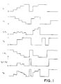
- two video signals V1 and V2 are multiplied by a key signal K1 (having a range of values from 0 to 1) and its complement (1 - K1) respectively, and the two signals V1K1 and V2(1 - K1) are additively combined in a summer to produce a composite output signal V q having the form V1K1 + V2(1 - K1).
- K1 having a range of values from 0 to 1
- V1K1 and V2(1 - K1 the two signals V1K1 and V2(1 - K1) are additively combined in a summer to produce a composite output signal V q having the form V1K1 + V2(1 - K1).
- K1 When the key signal K1 is zero, the input signal V1 makes no contribution to the signal V q , regardless of the value of V1. Similarly, if K1 is one, the signal V2 makes no contribution to the signal V q .
- the proportion of the signal V q that is contributed by V1 determines the opacity with which the scene represented by the signal V1 is perceived in the composite picture. If K1 is one, i.e., V1 represents 100% of the signal V q , then the V1 scene (the scene represented by the signal V1) completely obscures the V2 scene, regardless of the value of V2. As K1 decreases, the extent to which the V2 scene is obscured in the composite picture is reduced until, when K1 reaches zero, the V2 scene is opaque and completely obscures the V1 scene.
- the coefficients K1 and (1 - K1) determine the relative opacity of the two component scenes: if the coefficient K1 is greater than (1 - K1), then the V1 scene at least partially obscures the V2 scene and appears, to a viewer of the composite scene, to be in front of the V2 scene.
- FIG. 1 The multiplication of the signals V1 and V2 by the key signal K1 and its complement (1 - K1) is shown in FIG. 1, in which it is assumed that all signals have five discrete values in the range from zero to unity and have sharp transitions between levels. It will, of course, be appreciated that FIG. 1 is in fact very much simplified, and that in the case of analog signals the range of possible values is continuous, and that transitions for either analog or digital signals would have a finite slew rate.
- a video signal V1′ is said to be a "shaped" video signal when it is the multiplication product of an unshaped video signal V1 and an associated key signal K1. In general, there is no necessary relationship between the video signal and its associated key signal.
- a production switcher normally receives unshaped video signals and their associated key signals and provides a full screen video signal at its output. No key output is produced.
- the shaping of the component signals is discussed in terms of "coverage” in Porter, T. and Duff, T., “Compositing Digital Images", Computer Graphics, Vol. 18, No. 3 (1984), pages 253 to 259.
- V q V1K1 + V2K2 (1 - K1)
- V q V1K1 + V2K2 (1 - K1)
- V q ′ V1K1 + V2K2(1 - K1)
- the signal V2 makes no contribution to the signal V q ′, regardless of the value of K2. Therefore, combining of the video signals V1 and V2 is under the primary control of the key signal K1.
- the two different situations are equivalent respectively to the V1 scene and the V2 scene being in the foreground of the composite scene.
- the conventional mixer does not allow the operator to control on a dynamic basis whether the mixing operation is under the primary control of the signal K1 or of the signal K2 and an apparatus for combining video signals providing such control is the subject of co-pending EP-A-0236943.
- GB-A-2155729 discloses a video combiner in which unshaped video inputs are respectively applied to multipliers where the unshaped video signals are shaped by a key signal, and the outputs of the multipliers are further processed.
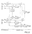
- the combiner cell shown in FIG. 2 comprises multipliers 4, 6, 8, 10 and 12, complement circuits 14, 16, 18, 20, 22 and 24, and a summer 26.
- the illustrated combiner cell operates in the digital domain with parallel data, and therefore all the signal lines that are illustrated would in fact be multiple conductor lines. Additional circuitry would be required to assure proper timing relationships among the various signals, but such matters are well within the skill of the art and therefore are not shown and will not be further described.
- the input signals of the combiner cell comprise two shaped video signals V1′ and V2′, associated key signals K1 and K2, and a priority signal P12.
- the levels of the key signals K1 and K2 and the level of the priority signal P12 are normalized to have maximum and minimum values that can be represented numerically as 1 and 0.
- the video signals V1′ and V2′ have the same maximum and minimum values.
- Additional multipliers 2 and 3 are provided upstream of the combiner for generating the shaped video signals V1′ and V2′ from unshaped video signals V1 and V2 and the associated key signals K1 and K2.
- the combiner cell provides a shaped output video signal V3′ and an output key signal K3.
- P12 determines the weighting factors that are applied to the two video signals V1′ and V2′. If P12 is equal to zero, this implies that the V2 scene is in the foreground of the composite scene and that the V1 scene is in the background, and vice versa if P12 is equal to one.
- V3′ V1′(1-K2)+V2′
- V3′ V2′(1-K1)+V1′
- V3′ V1′(1-K2/2)+V2′(1-K1/2)
- the priority signal P12 makes it possible to determine which of the component scenes will appear as the foreground scene in the composite picture.
- the composite picture can be changed so that a component scene is the foreground scene at one time and is the background scene at another time.
- combiner cells 30, 40 . . . 90 of the kind shown in FIG. 2 may be connected in cascade, as shown in FIG. 3, to form a combiner system.
- Output processors 32, 42 . . . 92 are associated with the combiner cells respectively, for a reason which will be explained below.
- the output signals from the output processors are connected to a production switcher.
- Conventional production switchers are designed to receive unshaped video signals and their associated key signals, and multiply the video signals by their key signals to produce shaped video signals that are combined with other shaped video signals, e.g., a signal generated by a digital video effects unit, to produce a final program video signal representing the desired composite picture.
- the output video signals provided by the combiner cells are already shaped by their respective key signals. If the signal V3′, for example, is applied to a conventional production switcher it will be shaped a second time, and the result will be a black halo in the scene represented by the signal V3′ for values of K3 greater than zero and less than unity.
- the output processors are interposed between the combiner cells and the production switcher in order to generate unshaped video signals from the shaped video signals generated by the combiner cells.
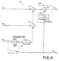
- FIG. 4 shows a processing circuit associated with the combiner cell 30.
- the output processing circuit 32 receives the shaped video signal V3′ and the key signal K3 from the associated combiner cell 30, and also receives a video matte signal M3.
- the signal M3 represents a background for the V3 scene.
- the background may be, for example, a plain, solid color.
- the output processor comprises a summer 102, a multiplier 104, a divider 106 (implemented as a reciprocal look-up table 108 and a multiplier 110) and a complement circuit 112.
- the processor comprises a switch 114 for selecting one of two operating modes for the processor.
- the processor provides a composite output video signal V3 ⁇ and a composite output key signal K3′, which are applied as input signals to the production switcher.
- V3 ⁇ V3′ + M3(1 - K3).
- the output key signal K3′ is set to unity for the entire frame in order to inhibit the production switcher from attempting to add another background.
- the output key signal K3′ is equal to K3, and the production switcher will then add background to pixels for which K3′ is not 1.0 in proportion to the value of (1 - K3).
- the signal V3 ⁇ is equal to V3 (which does not actually exist), and the switcher may multiply the signal V3 ⁇ by K3′ (which is equal to K3) and produce the desired signal V3′ at the switcher output.
- K3′ which is equal to K3
- V3 ⁇ is indeterminate, but this is not important to the final program video signal because these pixels make no contribution to that signal.
- the key and video output signals of the last combiner cell in the cascade are connected as inputs to the first combiner cell, so as to establish a closed ring.
- This provides additional flexibility, in that the ring can be logically broken at any point, allowing additional priority combinations.
- the signal V4′ can only be combined with the composite signal V1′/V2′, and the component signal V9′ can only be combined with the composite signal V1′/ . . ./V8′.
- the scene represented by the signal V9′ cannot be made to appear behind the V1 scene but in front of the V4 scene.
- the switches 94 are operated so that the output signals V9′ and K9 are applied to the combiner cell 30 in lieu of the input signals V2′ and K2, and P12 and P34 are set to unity, the desired composite signal would be provided at the output of the output processor 42 (V5 ⁇ , K5′).
- the key signal K8 must be forced to zero inside the combiner cell 90.
Description
- This invention relates to a processing circuit for video signals.
- In a video mixer, two video signals V₁ and V₂ (FIG. 1) are multiplied by a key signal K₁ (having a range of values from 0 to 1) and its complement (1 - K₁) respectively, and the two signals V₁K₁ and V₂(1 - K₁) are additively combined in a summer to produce a composite output signal Vq having the form V₁K₁ + V₂(1 - K₁). When the key signal K₁ is zero, the input signal V₁ makes no contribution to the signal Vq, regardless of the value of V₁. Similarly, if K₁ is one, the signal V₂ makes no contribution to the signal Vq. The proportion of the signal Vq that is contributed by V₁ determines the opacity with which the scene represented by the signal V₁ is perceived in the composite picture. If K₁ is one, i.e., V₁ represents 100% of the signal Vq, then the V₁ scene (the scene represented by the signal V₁) completely obscures the V₂ scene, regardless of the value of V₂. As K₁ decreases, the extent to which the V₂ scene is obscured in the composite picture is reduced until, when K₁ reaches zero, the V₂ scene is opaque and completely obscures the V₁ scene. Thus, the coefficients K₁ and (1 - K₁) determine the relative opacity of the two component scenes: if the coefficient K₁ is greater than (1 - K₁), then the V₁ scene at least partially obscures the V₂ scene and appears, to a viewer of the composite scene, to be in front of the V₂ scene.
- The multiplication of the signals V₁ and V₂ by the key signal K₁ and its complement (1 - K₁) is shown in FIG. 1, in which it is assumed that all signals have five discrete values in the range from zero to unity and have sharp transitions between levels. It will, of course, be appreciated that FIG. 1 is in fact very much simplified, and that in the case of analog signals the range of possible values is continuous, and that transitions for either analog or digital signals would have a finite slew rate.
- A video signal V₁′ is said to be a "shaped" video signal when it is the multiplication product of an unshaped video signal V₁ and an associated key signal K₁. In general, there is no necessary relationship between the video signal and its associated key signal. A production switcher normally receives unshaped video signals and their associated key signals and provides a full screen video signal at its output. No key output is produced.
- Shaping has two aspects, namely spatial or X - Y shaping (only the X-dimension is shown in FIG. 1), which determines the area of the composite picture to which the component signal makes a contribution (when K₁ = 0, the signal V₁ makes no contribution to the signal Vq), and opacity or Z shaping, which determines, for K₁ greater than zero, the magnitude of the contribution that is made by the component signal to the composite signal Vq. The shaping of the component signals is discussed in terms of "coverage" in Porter, T. and Duff, T., "Compositing Digital Images", Computer Graphics, Vol. 18, No. 3 (1984), pages 253 to 259.
- The foregoing discussion of the manner of production of the signal Vq is based on the assumption that the signal V₂ is a full field signal, i. e. that the key signal K₂ associated with the video signal V₂ is one for all locations. In the general case, K₂ is not one for all locations and

It will be seen from this more general expression that the video signal Vq, being the weighted sum of two shaped video signals V₁K₁ and V₂K₂, is itself a shaped video signal. For the sake of consistency in notation, the shaped signal that has previously been designated Vq will hereafter be designated Vq′, and Vq will hereafter be used to designate the corresponding unshaped signal. - The key signal Kq that relates Vq′ to Vq is given by

If, for every location, either K₁ or K₂ is one, then Kq = 1 for all locations. In particular, if either V₁ or V₂ is a full field signal, the signal Vq′ is a full field signal. If, on the other hand, Vq′ is not a full field signal it might be desired to form a composite scene from the scenes represented by the signal Vq′ and, e.g., a background scene represented by a signal Vr having an associated key signal Kr. In such a case, the signal (1- Kq) would be used to process the signal Vr in a production switcher, and an output signal Vs′ = Vq′ + VrKr (1 - Kq) would be produced. Generally, Vr would be a full field signal and so Kr = 1 and Vs′ = Vq′ + Vr(1 - Kq). - Recalling that Vq′ = V₁K₁ + V₂K₂(1 - K₁), if K₁ = 1, then Vq′ = V₁, i.e. the signal V₂ makes no contribution to the signal Vq′, regardless of the value of K₂. Therefore, combining of the video signals V₁ and V₂ is under the primary control of the key signal K₁. Similarly, if the signal Vq′ were equal to V₁K₁ (1 - K2) + V₂K₂, the combining would be under the primary control of the signal K₂, and if K₂ = 1, then Vq′ = V₂ and V₁ makes no contribution regardless of the value of K₁. The two different situations are equivalent respectively to the V₁ scene and the V₂ scene being in the foreground of the composite scene. However, the conventional mixer does not allow the operator to control on a dynamic basis whether the mixing operation is under the primary control of the signal K₁ or of the signal K₂ and an apparatus for combining video signals providing such control is the subject of co-pending EP-A-0236943.
- In passing, reference is made to GB-A-2155729 which discloses a video combiner in which unshaped video inputs are respectively applied to multipliers where the unshaped video signals are shaped by a key signal, and the outputs of the multipliers are further processed.
- According to this invention there is provided a processing circuit for receiving a shaped video signal V₃′ and an associated key signal K₃ and providing output signals in response thereto, said processing circuit having at least a first mode of operation and comprising first means operative in the first mode of the processing circuit to generate from the shaped video signal V₃˝ and the associated key signal K₃ an output video signal V₃˝ given by

where A is a function of the associated key signal and is independent of V₃′, and second means operative in the first mode to generate an output key signal having a constant value. - For a better understanding of the invention, and to show how the same may be carried into effect, reference will now be made, by way of example, to the accompanying drawings in which:
- FIG. 1 shows waveforms to illustrate combining of video signals,
- FIG. 2 is a block diagram of a combiner cell for combining first and second component video signals,
- FIG. 3 is a block diagram of a combiner system comprising several combiner cells connected in a cascade arrangement, and
- FIG. 4 is a block diagram of an output processing circuit for a combiner cell in accordance with the invention.
- The combiner cell shown in FIG. 2 comprises
multipliers complement circuits summer 26. The illustrated combiner cell operates in the digital domain with parallel data, and therefore all the signal lines that are illustrated would in fact be multiple conductor lines. Additional circuitry would be required to assure proper timing relationships among the various signals, but such matters are well within the skill of the art and therefore are not shown and will not be further described. - The input signals of the combiner cell comprise two shaped video signals V₁′ and V₂′, associated key signals K₁ and K₂, and a priority signal P₁₂. The levels of the key signals K₁ and K₂ and the level of the priority signal P₁₂ are normalized to have maximum and minimum values that can be represented numerically as 1 and 0. Also, the video signals V₁′ and V₂′ have the same maximum and minimum values.
Additional multipliers 2 and 3 are provided upstream of the combiner for generating the shaped video signals V₁′ and V₂′ from unshaped video signals V₁ and V₂ and the associated key signals K₁ and K₂. The combiner cell provides a shaped output video signal V₃′ and an output key signal K₃. It can readily be seen that the output video signal is given by the equation
and that the output key signal is given by
- The value of P₁₂ determines the weighting factors that are applied to the two video signals V₁′ and V₂′. If P₁₂ is equal to zero, this implies that the V₂ scene is in the foreground of the composite scene and that the V₁ scene is in the background, and vice versa if P₁₂ is equal to one.
- For P₁₂=0, then

- The value of K₂ defines areas in which the V₂ scene contributes to the composite scene. If K₂=1, the contribution of V₁ to the composite scene is zero and therefore the V₂ scene completely obscures the V₁ scene. If K₂=0, V₂′=0 and therefore there is no contribution from V₂ and V₁ is allowed to pass to V₃′ unaltered
- For P₁₂=1, then

- The value of K₁ defines areas in which the V₁ scene contributes to the composite scene. If K₁=1, the contribution of V₂ to the composite scene is zero and therefore the V₁ scene completely obscures the V₂ scene. If K₁=0, there is no contribution from V₁ and V₂ is allowed to pass to V₃′ unaltered.
- For P₁₂=0.5, then

- Where K₂=0, V₁′ is passed unaltered; where K₁=0, V₂′ is passed unaltered; and where K₂ > 0 and K₁ > 0, the relative opacities of the V₁ and V₂ scenes are determined by the ratio of K₁ and K₂.
- As P₁₂ increases from zero the relative depths of the V₁ and V₂ pixels in the composite image change, from the V₂ pixel appearing in front of the V₁ pixel, through the two pixels appearing to be at the same depth (at P₁₂=0.5), to the V₁ pixel appearing in front of the V₂ pixel. It will therefore be seen that the priority signal P₁₂ makes it possible to determine which of the component scenes will appear as the foreground scene in the composite picture. By changing the value of P₁₂, the composite picture can be changed so that a component scene is the foreground scene at one time and is the background scene at another time.
-
Several combiner cells Output processors - Conventional production switchers are designed to receive unshaped video signals and their associated key signals, and multiply the video signals by their key signals to produce shaped video signals that are combined with other shaped video signals, e.g., a signal generated by a digital video effects unit, to produce a final program video signal representing the desired composite picture. The output video signals provided by the combiner cells are already shaped by their respective key signals. If the signal V₃′, for example, is applied to a conventional production switcher it will be shaped a second time, and the result will be a black halo in the scene represented by the signal V₃′ for values of K₃ greater than zero and less than unity. The output processors are interposed between the combiner cells and the production switcher in order to generate unshaped video signals from the shaped video signals generated by the combiner cells.
- FIG. 4 shows a processing circuit associated with the
combiner cell 30. The other output processing circuits are identical. As shown in FIG. 4, theoutput processing circuit 32 receives the shaped video signal V₃′ and the key signal K₃ from the associatedcombiner cell 30, and also receives a video matte signal M₃. The signal M₃ represents a background for the V₃ scene. The background may be, for example, a plain, solid color. The output processor comprises asummer 102, amultiplier 104, a divider 106 (implemented as a reciprocal look-up table 108 and a multiplier 110) and acomplement circuit 112. In addition, the processor comprises aswitch 114 for selecting one of two operating modes for the processor. The processor provides a composite output video signal V₃˝ and a composite output key signal K₃′, which are applied as input signals to the production switcher. - In the first mode of operation of the processor (background on), the signal V₃˝ is given by

Thus, for any pixel for which K₃ is zero, V₃′ = 0 and V₃˝ = M₃. If K₃ is not zero, indicating that V₃′ is non-zero, the relative contribution of V₃′ to V₃˝ depends on the value of K₃, and it can be seen that for K₃ = 1, M₃ is not permitted to make a contribution and V₃˝ = V₃′. The output key signal K₃′ is set to unity for the entire frame in order to inhibit the production switcher from attempting to add another background. - In the second mode of operation (background off), the output key signal K₃′ is equal to K₃, and the production switcher will then add background to pixels for which K₃′ is not 1.0 in proportion to the value of (1 - K₃). The production switcher will multiply V₃˝ by K₃′. Since K₃′ is equal to K₃, it is desired for the reason indicated above that V₃˝ not be equal to V₃′. Therefore, in the second mode the output signal V₃′ from the
summer 102 is divided by the key signal K₃, so that
Therefore, the signal V₃˝ is equal to V₃ (which does not actually exist), and the switcher may multiply the signal V₃˝ by K₃′ (which is equal to K₃) and produce the desired signal V₃′ at the switcher output. For pixels at which K₃ is close to zero, V₃˝ is indeterminate, but this is not important to the final program video signal because these pixels make no contribution to that signal. - It will be appreciated that the invention is not restricted to the particular apparatus that has been described and illustrated, and that variations may be made therein without departing from the scope of the invention as defined in the appended claims, and equivalents thereof. For example, instead of using interdependent processing circuits for generating, from K₁, K₂ and P₁₂, the multiplication factors for the video signals V₁ and V₂, these multiplication factors may be generated independently, as mix constants that are separately applied to the multipliers of a signal mixer that is of otherwise conventional form. It is not necessary that each combiner cell of the system shown in FIG. 3 should have its own output processor, since if the output is always to be taken from the same combiner cell, it is necessary only that an output processor be associated with that combiner cell. In a preferred implementation of the invention, the key and video output signals of the last combiner cell in the cascade are connected as inputs to the first combiner cell, so as to establish a closed ring. This provides additional flexibility, in that the ring can be logically broken at any point, allowing additional priority combinations. For example, in the arrangement shown in FIG. 3 the signal V₄′ can only be combined with the composite signal V₁′/V₂′, and the component signal V₉′ can only be combined with the composite signal V₁′/ . . ./V₈′. The scene represented by the signal V₉′ cannot be made to appear behind the V₁ scene but in front of the V₄ scene. However, if the
switches 94 are operated so that the output signals V₉′ and K₉ are applied to thecombiner cell 30 in lieu of the input signals V₂′ and K₂, and P₁₂ and P₃₄ are set to unity, the desired composite signal would be provided at the output of the output processor 42 (V₅˝, K₅′). The key signal K₈ must be forced to zero inside thecombiner cell 90. - It will also be appreciated that although the preferred embodiment of the invention, described above with reference to the drawings, is implemented using parallel digital data, it could also be implemented using serial digital data or analog data.
Claims (3)
- A processing circuit (32,42,92) for receiving a shaped video signal V₃′ and an associated key signal K₃ and providing output signals in response thereto, said processing circuit having at least a first mode of operation and comprising first means (102-112) operative in the first mode of the processing circuit to generate from the shaped video signal V₃′ and the associated key signal K₃ an output video signal V₃˝ given by

- A processing circuit according to claim 1, having a second mode of operation, and wherein the first means (102-112) are operative in the second mode to generate an output video signal V₃˝ given by

- A processing circuit according to claim 1, wherein said processing circuit has an input terminal for receiving a matte signal M₃ and is operative in the first mode to generate an output video signal V₃˝ given by

Applications Claiming Priority (3)
| Application Number | Priority Date | Filing Date | Title |
|---|---|---|---|
| US83694586A | 1986-03-06 | 1986-03-06 | |
| US836945 | 1986-03-06 | ||
| EP87103109A EP0236943B1 (en) | 1986-03-06 | 1987-03-05 | Apparatus for combining video signals |
Related Parent Applications (2)
| Application Number | Title | Priority Date | Filing Date |
|---|---|---|---|
| EP87103109A Division EP0236943B1 (en) | 1986-03-06 | 1987-03-05 | Apparatus for combining video signals |
| EP87103109.2 Division | 1987-03-05 |
Publications (3)
| Publication Number | Publication Date |
|---|---|
| EP0486468A2 EP0486468A2 (en) | 1992-05-20 |
| EP0486468A3 EP0486468A3 (en) | 1992-06-03 |
| EP0486468B1 true EP0486468B1 (en) | 1995-04-19 |
Family
ID=25273108
Family Applications (2)
| Application Number | Title | Priority Date | Filing Date |
|---|---|---|---|
| EP92100535A Expired - Lifetime EP0486468B1 (en) | 1986-03-06 | 1987-03-05 | Processing circuit for video signals |
| EP87103109A Expired - Lifetime EP0236943B1 (en) | 1986-03-06 | 1987-03-05 | Apparatus for combining video signals |
Family Applications After (1)
| Application Number | Title | Priority Date | Filing Date |
|---|---|---|---|
| EP87103109A Expired - Lifetime EP0236943B1 (en) | 1986-03-06 | 1987-03-05 | Apparatus for combining video signals |
Country Status (4)
| Country | Link |
|---|---|
| EP (2) | EP0486468B1 (en) |
| JP (1) | JPH0771220B2 (en) |
| CA (1) | CA1309768C (en) |
| DE (2) | DE3785871T2 (en) |
Families Citing this family (13)
| Publication number | Priority date | Publication date | Assignee | Title |
|---|---|---|---|---|
| CA1310771C (en) * | 1987-05-18 | 1992-11-24 | Ivan J. Maltz | Video compositing using a software linear keyer |
| US4823183A (en) * | 1988-02-01 | 1989-04-18 | The Grass Valley Group, Inc. | Video mixer with multicolor boarder |
| US4873568A (en) * | 1988-09-19 | 1989-10-10 | The Grass Valley Group, Inc. | Digital video effects apparatus |
| DE3842978C2 (en) * | 1988-12-21 | 1996-04-11 | Broadcast Television Syst | Mixing device for video signals |
| DE3842977C2 (en) * | 1988-12-21 | 1996-03-28 | Broadcast Television Syst | Mixing device for video signals |
| US4947254A (en) * | 1989-04-27 | 1990-08-07 | The Grass Valley Group, Inc. | Layered mix effects switcher architecture |
| EP0498647A3 (en) * | 1991-02-11 | 1993-08-25 | Ampex Corporation | Keyed, true-transparency image information combine |
| GB9109999D0 (en) * | 1991-05-09 | 1991-07-03 | Quantel Ltd | Improvements in or relating to keying systems and methods for television image processing |
| US5351067A (en) * | 1991-07-22 | 1994-09-27 | International Business Machines Corporation | Multi-source image real time mixing and anti-aliasing |
| JP3198656B2 (en) * | 1992-08-31 | 2001-08-13 | ソニー株式会社 | Video signal synthesizing apparatus and method |
| JPH06141235A (en) * | 1992-10-22 | 1994-05-20 | Sony Corp | Video signal processor |
| JP3301679B2 (en) * | 1994-12-07 | 2002-07-15 | 松下電器産業株式会社 | Video composition circuit |
| DE10236338A1 (en) * | 2002-08-08 | 2004-02-19 | Bts Media Solutions Gmbh | Device for mixing video signals has mixing stage groups, whereby each 2 video signals are added after multiplying by control signals, changeover switches, all mixer stages connected to device outputs |
Family Cites Families (4)
| Publication number | Priority date | Publication date | Assignee | Title |
|---|---|---|---|---|
| JPS60139377U (en) * | 1984-02-25 | 1985-09-14 | ソニー株式会社 | Video signal mix circuit |
| GB8405947D0 (en) * | 1984-03-07 | 1984-04-11 | Quantel Ltd | Video signal processing systems |
| US4758892A (en) * | 1984-04-27 | 1988-07-19 | Ampex Corporation | System for producing a video combine from multiple video images |
| EP0217938B1 (en) * | 1985-04-12 | 1993-06-16 | Ampex Corporation | Apparatus and method for processing previously processed video signals |
-
1987
- 1987-02-05 CA CA000529089A patent/CA1309768C/en not_active Expired - Fee Related
- 1987-02-27 JP JP62045074A patent/JPH0771220B2/en not_active Expired - Lifetime
- 1987-03-05 EP EP92100535A patent/EP0486468B1/en not_active Expired - Lifetime
- 1987-03-05 EP EP87103109A patent/EP0236943B1/en not_active Expired - Lifetime
- 1987-03-05 DE DE19873785871 patent/DE3785871T2/en not_active Expired - Fee Related
- 1987-03-05 DE DE19873751262 patent/DE3751262T2/en not_active Expired - Fee Related
Also Published As
| Publication number | Publication date |
|---|---|
| CA1309768C (en) | 1992-11-03 |
| DE3785871D1 (en) | 1993-06-24 |
| EP0236943A2 (en) | 1987-09-16 |
| EP0486468A2 (en) | 1992-05-20 |
| DE3751262T2 (en) | 1995-12-21 |
| DE3785871T2 (en) | 1993-11-11 |
| JPS62213386A (en) | 1987-09-19 |
| EP0236943B1 (en) | 1993-05-19 |
| DE3751262D1 (en) | 1995-05-24 |
| EP0486468A3 (en) | 1992-06-03 |
| JPH0771220B2 (en) | 1995-07-31 |
| EP0236943A3 (en) | 1989-08-09 |
Similar Documents
| Publication | Publication Date | Title |
|---|---|---|
| US4851912A (en) | Apparatus for combining video signals | |
| EP0486468B1 (en) | Processing circuit for video signals | |
| JP3198656B2 (en) | Video signal synthesizing apparatus and method | |
| EP0334475A1 (en) | Video switcher with independent processing of selected video signals | |
| US5416529A (en) | Method and system for digital video processing with combined downstream keyer and fade to black mixer | |
| JPH0473189B2 (en) | ||
| US5305107A (en) | Combining digital video key signals | |
| US4879597A (en) | Processing of video image signals | |
| JP2709523B2 (en) | Mixed effect switcher device | |
| EP0716541B1 (en) | A video mixing apparatus | |
| EP0217938B1 (en) | Apparatus and method for processing previously processed video signals | |
| JP2946160B2 (en) | Video signal shadowing method | |
| US5644365A (en) | Method and circuit for generating a composite video signal | |
| US5285283A (en) | Depth signal processing in a video switcher | |
| EP0314250A2 (en) | Video digital analog signal processing and display | |
| JP2782432B2 (en) | Video signal processing device | |
| CA1323689C (en) | Apparatus for combining video signals | |
| US5502505A (en) | Special effect video apparatus for achieving extended dimming and fading effects | |
| EP0506430B1 (en) | Apparatus and method for combining video signals | |
| JPH04220693A (en) | Digital-image mixing apparatus in picture element | |
| EP0498647A2 (en) | Keyed, true-transparency image information combine | |
| JP3350968B2 (en) | Video signal synthesizer | |
| JPH0530389A (en) | Blanking level signal generating circuit | |
| JPS60169280A (en) | Profile compensating device | |
| JP2003060987A (en) | Image signal compositing apparatus and method |
Legal Events
| Date | Code | Title | Description |
|---|---|---|---|
| PUAI | Public reference made under article 153(3) epc to a published international application that has entered the european phase |
Free format text: ORIGINAL CODE: 0009012 |
|
| PUAL | Search report despatched |
Free format text: ORIGINAL CODE: 0009013 |
|
| AC | Divisional application: reference to earlier application |
Ref document number: 236943 Country of ref document: EP |
|
| AK | Designated contracting states |
Kind code of ref document: A2 Designated state(s): DE FR GB |
|
| AK | Designated contracting states |
Kind code of ref document: A3 Designated state(s): DE FR GB |
|
| 17P | Request for examination filed |
Effective date: 19920902 |
|
| 17Q | First examination report despatched |
Effective date: 19940818 |
|
| GRAA | (expected) grant |
Free format text: ORIGINAL CODE: 0009210 |
|
| AC | Divisional application: reference to earlier application |
Ref document number: 236943 Country of ref document: EP |
|
| AK | Designated contracting states |
Kind code of ref document: B1 Designated state(s): DE FR GB |
|
| PG25 | Lapsed in a contracting state [announced via postgrant information from national office to epo] |
Ref country code: FR Effective date: 19950419 |
|
| REF | Corresponds to: |
Ref document number: 3751262 Country of ref document: DE Date of ref document: 19950524 |
|
| EN | Fr: translation not filed | ||
| PLBE | No opposition filed within time limit |
Free format text: ORIGINAL CODE: 0009261 |
|
| STAA | Information on the status of an ep patent application or granted ep patent |
Free format text: STATUS: NO OPPOSITION FILED WITHIN TIME LIMIT |
|
| 26N | No opposition filed | ||
| PGFP | Annual fee paid to national office [announced via postgrant information from national office to epo] |
Ref country code: DE Payment date: 19990226 Year of fee payment: 13 |
|
| PG25 | Lapsed in a contracting state [announced via postgrant information from national office to epo] |
Ref country code: DE Free format text: LAPSE BECAUSE OF NON-PAYMENT OF DUE FEES Effective date: 20010103 |
|
| REG | Reference to a national code |
Ref country code: GB Ref legal event code: IF02 |
|
| PGFP | Annual fee paid to national office [announced via postgrant information from national office to epo] |
Ref country code: GB Payment date: 20020417 Year of fee payment: 16 |
|
| PG25 | Lapsed in a contracting state [announced via postgrant information from national office to epo] |
Ref country code: GB Free format text: LAPSE BECAUSE OF NON-PAYMENT OF DUE FEES Effective date: 20030305 |
|
| GBPC | Gb: european patent ceased through non-payment of renewal fee |
Effective date: 20030305 |