EP0486366A1 - Circuit to increase the information output rate in a data-exchange system - Google Patents
Circuit to increase the information output rate in a data-exchange system Download PDFInfo
- Publication number
- EP0486366A1 EP0486366A1 EP91402990A EP91402990A EP0486366A1 EP 0486366 A1 EP0486366 A1 EP 0486366A1 EP 91402990 A EP91402990 A EP 91402990A EP 91402990 A EP91402990 A EP 91402990A EP 0486366 A1 EP0486366 A1 EP 0486366A1
- Authority
- EP
- European Patent Office
- Prior art keywords
- badge
- transistor
- modem
- circuit
- fixed station
- Prior art date
- Legal status (The legal status is an assumption and is not a legal conclusion. Google has not performed a legal analysis and makes no representation as to the accuracy of the status listed.)
- Granted
Links
- 230000010365 information processing Effects 0.000 claims description 7
- 230000005669 field effect Effects 0.000 claims description 6
- 230000007423 decrease Effects 0.000 claims description 3
- 230000010287 polarization Effects 0.000 description 10
- 230000005540 biological transmission Effects 0.000 description 8
- 238000010586 diagram Methods 0.000 description 8
- 230000008859 change Effects 0.000 description 7
- 239000003990 capacitor Substances 0.000 description 5
- 230000004044 response Effects 0.000 description 5
- 230000003321 amplification Effects 0.000 description 4
- 238000003199 nucleic acid amplification method Methods 0.000 description 4
- 238000005265 energy consumption Methods 0.000 description 3
- 230000002618 waking effect Effects 0.000 description 3
- 230000006978 adaptation Effects 0.000 description 2
- 230000006872 improvement Effects 0.000 description 2
- 239000003607 modifier Substances 0.000 description 2
- 244000045947 parasite Species 0.000 description 2
- 230000035945 sensitivity Effects 0.000 description 2
- 241001080024 Telles Species 0.000 description 1
- 230000007175 bidirectional communication Effects 0.000 description 1
- 230000006854 communication Effects 0.000 description 1
- 238000004891 communication Methods 0.000 description 1
- 230000008878 coupling Effects 0.000 description 1
- 238000010168 coupling process Methods 0.000 description 1
- 238000005859 coupling reaction Methods 0.000 description 1
- 238000001514 detection method Methods 0.000 description 1
- 230000005670 electromagnetic radiation Effects 0.000 description 1
- 235000021183 entrée Nutrition 0.000 description 1
- 238000004519 manufacturing process Methods 0.000 description 1
- 238000000034 method Methods 0.000 description 1
- 230000008569 process Effects 0.000 description 1
- 230000009467 reduction Effects 0.000 description 1
- 230000006641 stabilisation Effects 0.000 description 1
- 238000011105 stabilization Methods 0.000 description 1
Images
Classifications
-
- G—PHYSICS
- G06—COMPUTING; CALCULATING OR COUNTING
- G06K—GRAPHICAL DATA READING; PRESENTATION OF DATA; RECORD CARRIERS; HANDLING RECORD CARRIERS
- G06K7/00—Methods or arrangements for sensing record carriers, e.g. for reading patterns
- G06K7/0008—General problems related to the reading of electronic memory record carriers, independent of its reading method, e.g. power transfer
-
- G—PHYSICS
- G01—MEASURING; TESTING
- G01S—RADIO DIRECTION-FINDING; RADIO NAVIGATION; DETERMINING DISTANCE OR VELOCITY BY USE OF RADIO WAVES; LOCATING OR PRESENCE-DETECTING BY USE OF THE REFLECTION OR RERADIATION OF RADIO WAVES; ANALOGOUS ARRANGEMENTS USING OTHER WAVES
- G01S13/00—Systems using the reflection or reradiation of radio waves, e.g. radar systems; Analogous systems using reflection or reradiation of waves whose nature or wavelength is irrelevant or unspecified
- G01S13/74—Systems using reradiation of radio waves, e.g. secondary radar systems; Analogous systems
- G01S13/76—Systems using reradiation of radio waves, e.g. secondary radar systems; Analogous systems wherein pulse-type signals are transmitted
- G01S13/767—Responders; Transponders
Definitions
- the present invention relates to a system for transmitting data by modulation-demodulation of an electromagnetic wave, for bidirectional communication between a fixed station, known as a beacon or reader, and a mobile station, known as a badge or answering machine. More specifically, the invention relates to the modem (modulator-demodulator) of the portable badge, for which an improvement brought by the invention makes it possible to pass from the standby state, to which correspond a low consumption but also a low data rate, to an active state, to which correspond a higher consumption but a high data rate, multiplied by a factor of the order of 100 or several hundred.
- This type of data exchange finds its applications in the control of mobiles, such as identification of wagons on a track, automobiles at a toll or pedestrians at a building entrance.
- the mobile station or badge looks like a smart card, and it must be extremely energy efficient, since it is powered by small batteries called "buttons".
- a mobile station or badge 1 comprises a microwave part 3, an information processing part 4 and a power supply 5.
- the exchanges between these two parts relate to modulation-demodulation and transmission / reception commands.
- the fixed station or beacon 2 comprises a microwave source, a microwave part 6, an information processing part 7, and a computer 8 which makes it possible to manage all of the radioelectric exchanges carried out with the badges, via the antennas 9 for each badge and 10 for the tag or reader.
- modulations used in these systems are generally of the OOK type (in On-Off-Keying amplitude modulation), of the PSK type (in O / ⁇ Phase-Shift-Keying phase modulation), or FSK (Frequency Shift Keying).
- the operation of the modem is not the same depending on whether the tag interrogates the badge or whether the badge responds to the tag.
- the badge In the direction of interrogation of the badge 1 by the reader 2, the latter generates (P li ) a modulated microwave signal.
- the badge receives this signal (P br ) and demodulates it: it is a step which makes it possible to activate the badge which was in the standby state.
- the reader In the direction of the response from badge 1 to reader 2, the reader then generates an unmodulated microwave signal.
- the badge receives this signal, the module - that is to say the load of information about which it has been interrogated - and re-emits a signal comprising, as appropriate, either losses or gain.
- a high rate of information in turn requires that the modulation function of the modem be at low impedance, which moreover corresponds to higher energy consumption during the duration of the response from the badge to the reader.
- the badge in the standby state, transmits to its processing circuit 4 a series of information at low bit rates, which are identified by said circuit as an interrogation originating from the reader 2.
- the processing circuit 4 of the badge then "wakes up" the modem 3 by transmitting signals which act on means which modify the impedance or impedances of the modem, and allow it to respond with a high flow of information to the interrogation of the reader.
- the invention relates to a circuit for increasing the rate of information by microwave electromagnetic waves, in a data exchange system between a fixed station and a mobile station, called a portable badge, which includes a modem and an information processing circuit which is under high impedance and low consumption electric in the standby state, when the fixed station does not transmit a signal, this circuit being characterized in that, as soon as the fixed station transmits an interrogation signal with a low information rate (kilobits / sec), transmitted by the modem to the processing circuit, the latter emits a "wake-up" signal from the modem which acts on means reducing the modem's output impedance, thereby increasing the information rate (mega bits / sec) exchanged with the fixed station.
- a portable badge which includes a modem and an information processing circuit which is under high impedance and low consumption electric in the standby state, when the fixed station does not transmit a signal
- this circuit being characterized in that, as soon as the fixed station transmits an interrogation signal with a low information rate (
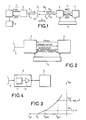
- FIG. 2 repeats the part of the badge 1 of FIG. 1, but shows a new link between the modem 3 and the information processing circuit 4.
- the transmission rates are generally limited in the direction from the reader to the badge. Indeed, although there is no particular problem for a reader to transmit at high speed, because its consumption does not matter, on the other hand if the badge demodulation function is unique, there is only one only energy state, this must be carried out at very high impedance, because it corresponds to the standby state under very low energy consumption - because of the "button" batteries which supply the badge.
- the time constants linked to the high impedances of the modem 3 and to the input capacities of the processing circuit 4, limit the demodulation rate to a few tens of kilobits / second.
- This low speed is sufficient to activate the information processing circuit 4, but insufficient to ensure data exchange between a reader and a plurality of badges: several megabits / second are necessary.
- the processing circuit 4 when the processing circuit 4 detects an interrogation coming from the reader 2, it sends to the modem 3 of the badge a signal which "wakes it up", and lowers its characteristic impedances, thus authorizing a high flow of information.
- the badge wake-up process is based on a change in the bias point of the transistor which functions as a detector in the modem 3.
- FIG. 3 gives the example of a field effect transistor, polarized on its gate at a voltage Vg sO close to the pinch voltage Vp: the transistor is in the standby state, and to this voltage V 9s0 corresponds a low drain current I ds , 2 ⁇ A for example.
- the gate bias voltage is switched to a higher value Vg s1 , to which corresponds a higher drain current I ds , for example between 10 and 100 ⁇ A, which decreases the impedances and time constants. If I ds goes from 2pA to 20pA the information rate is multiplied by 10.
- one (or more) amplifier 31 can be used, in series with the detector transistor 11, in the modem 3 , as shown in Figure 4: it is the amplifier which is "awakened", to transmit at high speed.
- the amplifier 31 works at the demodulation frequency, and its bias voltage is changed, while the transistor 11 continues to be in an optimal bias zone for the detection function.
- the basis of this arrangement consists in lowering the load impedance of the detector, therefore in increasing the information rate, without changing its point of polarization, and in compensating for the drop in level associated with the reduction in the output impedance by the change in polarization and therefore the increase in the gain of the amplifier 31 which follows the detector 11.
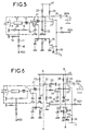
- FIG. 5 gives the detailed electrical diagram of a broadband modem, produced as an integrated circuit according to the invention, in which the polarization point of the transistor used as a detector is modified.
- the circuit shown is active in reception and passive in transmission, but other types of circuits can be adapted according to the invention.
- Capacities 15 and 22 are microwave decoupling capacities.
- Resistors 23 and 19 are of high values, of the order of 100 kn and 500 kn respectively. It is they which, in the standby state, polarize the drain and the source, and consequently determine Vg s and I ds .
- these two polarization resistors 23 and 19 are almost short-circuited by the two resistors 25 and 26, respectively, which are of the order of 10 k ⁇ , that is to say significantly lower in value than 100 and 500 k ⁇ .
- the switching between resistors 23 and 25, on the one hand, and 19 and 26, on the other hand, is carried out by means of transistors 27 and 28 respectively, when they are in the on state.
- These switching transistors 27 and 28 are controlled by the information processing circuit 4, by a signal applied to the wake-up terminal REV, and limited by the resistor 29.
- the resistor 30 sets the gates of the switching transistors 27 and 28 to -V, if these are not controlled or if the wake-up function is at high impedance: indeed, the high impedance state is often that of the logic gates d 'a processing circuit in "standby" mode. The transistors 27 and 28 are then blocked.
- the amplifier at the demodulation frequency essentially consists of at least one transistor 31, connected by means of a decoupling capacitor 32 to the load of the microwave transistor 11.
- the load LF of the transistor 11 is constituted by the resistance 23 (approximately 100 kn), the capacity 32 and the resistance 33 (approximately 500 k ⁇ - 1 M ⁇ ).
- Transistor 34 when controlled by the wake-up signal REV at the same time as transistors 27 and 28, switches the load LF of the detector transistor 11: its load resistance 33 (0.5 - -1 M ⁇ ) at 1 the standby state is shunted by the resistor 35 of low value (10 k ⁇ ) in the awakened state.
- the resistors 36 and 37 are stabilization resistors of the transistor 31 in the waking state: its drain load is constituted by the resistor 38 of high value (approximately 100 k ⁇ ) and the microwave decoupling capacity 39. Its source, decoupled by a capacitor 15, is self-polarized by a resistor 40 and a capacitor 41, in the same way as the source of the detector transistor 11: like the resistor 19, the resistor 40 has a high value, around 500 k ⁇ .
- FIG. 6 there is only one amplification stage, comprised between the lines AA and BB, between the detector stage and the wake-up stage by changing the polarization points. If the information rate requested from the badge must be higher than that supplied with a single amplification stage, there is no difficulty for those skilled in the art to cascade several amplification stages identical to that which is represented: it is only necessary to provide that each amplifier has its own wake-up stage, that is the transistors 27 and 28, and the associated circuits. The transistor 34, and its associated circuit 32 + 35, which switches the output impedance of the detector transistor 11, remains unique if there are several amplification stages. The demodulated DEM output is taken from the last amplifier.
- the two examples which have been exposed use a semi-active type modem.
- the invention is applicable to other types of modem, of which it suffices to change the polarization of the detector transistor.
- production in an integrated circuit does not limit the application of the invention, which can be carried out in a hybrid circuit, using microstrip lines which replace the inductors and the capacitors.
Landscapes
- Engineering & Computer Science (AREA)
- Remote Sensing (AREA)
- Radar, Positioning & Navigation (AREA)
- Physics & Mathematics (AREA)
- General Physics & Mathematics (AREA)
- Computer Networks & Wireless Communication (AREA)
- Theoretical Computer Science (AREA)
- Computer Vision & Pattern Recognition (AREA)
- Artificial Intelligence (AREA)
- Exchange Systems With Centralized Control (AREA)
- Radar Systems Or Details Thereof (AREA)
- Data Exchanges In Wide-Area Networks (AREA)
- Transceivers (AREA)
- Mobile Radio Communication Systems (AREA)
- Digital Transmission Methods That Use Modulated Carrier Waves (AREA)
Abstract
Description
La présente invention concerne un système de transmission de données par modulation- démodulation d'une onde électromagnétique, pourcommunica- tion bidirectionnelle entre une station fixe, dite balise ou lecteur, et une station mobile, dite badge ou répondeur. Plus précisément, l'invention concerne le modem (modulateur-démodulateur) du badge portable, pour lequel un perfectionnement apporté par l'invention permet de passer de l'état de veille, auquel correspondent une faible consommation mais aussi un faible débit de données, à un état actif, auquel correspondent une consommation plus élevée mais un fort débit de données, multiplié par un facteur de l'ordre de 100 ou plusieurs centaines.The present invention relates to a system for transmitting data by modulation-demodulation of an electromagnetic wave, for bidirectional communication between a fixed station, known as a beacon or reader, and a mobile station, known as a badge or answering machine. More specifically, the invention relates to the modem (modulator-demodulator) of the portable badge, for which an improvement brought by the invention makes it possible to pass from the standby state, to which correspond a low consumption but also a low data rate, to an active state, to which correspond a higher consumption but a high data rate, multiplied by a factor of the order of 100 or several hundred.
Ce type d'échange de données trouve ses applications dans le contrôle de mobiles, tel qu'identification de wagons sur une voie, d'automobiles à un péage ou de piétons à une entrée d'immeuble.This type of data exchange finds its applications in the control of mobiles, such as identification of wagons on a track, automobiles at a toll or pedestrians at a building entrance.
La station mobile ou badge se présente comme une carte à puce, et elle doit être extrêmement économe en énergie, car elle est alimentée par de petites piles dites "boutons".The mobile station or badge looks like a smart card, and it must be extremely energy efficient, since it is powered by small batteries called "buttons".
Le schéma d'ensemble d'un système d'échange de données par rayonnement électromagnétique ou hyperfréquences, selon l'art connu, est assez simple, et la figure 1 qui le représente permet d'en préciser les éléments, et les sigles utilisés.The overall diagram of a data exchange system by electromagnetic radiation or microwave, according to the known art, is quite simple, and Figure 1 which represents it allows to specify the elements, and the acronyms used.
Une station mobile ou badge 1 comprend une partie hyperfréquence 3, une partie traitement de l'information 4 et une alimentation 5. Les échanges entre ces deux parties concernent la modulation- démodulation et les commandes émission/réception.A mobile station or badge 1 comprises a
La station fixe ou balise 2 comprend une source hyperfréquence, une partie hyperfréquence 6, une partie de traitement de l'information 7, et un calculateur 8 qui permet de gérer l'ensemble des échanges radioélectriques effectués avec les badges, par l'intermédiaire des antennes 9 pour chaque badge et 10 pour la balise ou lecteur.The fixed station or
On utilisera :
- - d = distance entre les
antennes 9 et 10 - - G = gain de l'antenne 10 du
lecteur 2 - - Gb = gain de l'antenne 9 du badge 1
- - Pli = puissance émise à l'antenne du
lecteur 2 - - Plr = puissance reçue par l'antenne du lecteur
- - Pb; = puissance émise à l'antenne du badge 1
- - Pbr = puissance reçue par l'antenne du badge
- - d = distance between
antennas - - G = gain of
antenna 10 ofreader 2 - - G b = gain of
antenna 9 of badge 1 - - P li = power transmitted to the antenna of
reader 2 - - P lr = power received by the reader antenna
- - P b ; = power emitted at the antenna of badge 1
- - P br = power received by the badge antenna
Les modulations utilisées dans ces systèmes sont généralement de type OOK ( en modulation d'amplitude On-Off-Keying), de type PSK (en modulation de phase O/¶ Phase-Shift-Keying), ou FSK (Frequency Shift Keying).The modulations used in these systems are generally of the OOK type (in On-Off-Keying amplitude modulation), of the PSK type (in O / ¶ Phase-Shift-Keying phase modulation), or FSK (Frequency Shift Keying).
Le fonctionnement du modem n'est pas le même selon que la balise interroge le badge oui que le badge répond à la balise.The operation of the modem is not the same depending on whether the tag interrogates the badge or whether the badge responds to the tag.
Dans le sens de l'interrogation du badge 1 par le lecteur 2, celui-ci génère (Pli) un signal hyperfréquence modulé. Le badge reçoit ce signal (Pbr) et le démodule : c'est une étape qui permet d'activer le badge qui était à l'état de veille.In the direction of interrogation of the badge 1 by the
Dans le sens de la réponse du badge 1 au lecteur 2, le lecteur génère alors un signal hyperfréquence non modulé. Le badge reçoit ce signal, le module - c'est à dire le charge des informations au sujet desquelles il a été interrogé - et réémet un signal comportant, suivant le cas, soit des pertes, soit du gain.In the direction of the response from badge 1 to
En effet, le badge peut être:
- - passif, c'est à dire que la puissance qu'il émet est toujours inférieure à la puissance qu'il reçoit (Pbi<P br), et l'énergie lui est fournie par le lecteur,
- - ou actif, c'est à dire qu'il comprend un amplificateur hyperfréquence (Pbi > Pbr) , ce qui suppose donc une source d'alimentation telle que des piles . Il y a donc des problèmes de consommation d'énergie tout au moins du côté du badge, qui équivalent à des problèmes d'obtention de sensibilité du badge à l'état de veille, donc sous très faible consommation, et de sensibilité du lecteur compte tenu du faible niveau d'émission du badge, et des parasites apportés par d'autres systèmes fonctionnant à une fréquence proche.
- - passive, that is to say that the power it emits is always less than the power it receives (P bi <P br ), and the energy is supplied to it by the reader,
- - or active, that is to say that it comprises a microwave amplifier (P bi > P br ), which therefore assumes a power source such as batteries. There are therefore problems of energy consumption at least on the badge side, which is equivalent to problems of obtaining sensitivity of the badge in the standby state, therefore under very low consumption, and sensitivity of the reader account given the low emission level of the badge, and parasites brought by other systems operating at a close frequency.
Mais en outre, il y a des problèmes de débits d'informations numériques. L'économie d'énergie lorsque le badge est à l'état de veille - ce qui est son état le plus courant -impose que la fonction de démodulation soit réalisée sous très haute impédance : les constantes de temps, liées aux impédances et aux capacités d'entrées des circuits, limitent les débits à quelques dizaines de kilobits/seconde, par exemple.But in addition, there are problems with digital information rates. Saving energy when the badge is in standby state - which is its most common state - requires that the demodulation function be performed under very high impedance: time constants, linked to impedances and capacities of circuit inputs, limit bit rates to a few tens of kilobits / second, for example.
Ces débits ne sont pas suffisants pour assurer un trafic d'informations normal entre une station fixe et plusieurs stations mobiles ou badges : il faut atteindre plusieurs mégabits/seconde, dès que le badge est "réveillé", et qu'il entre en communication avec le lecteur.These rates are not sufficient to ensure normal information traffic between a fixed station and several mobile stations or badges: it is necessary to reach several megabits / second, as soon as the badge is "awakened", and that it enters into communication with the reader.
Un fort débit d'informations impose à son tour que la fonction modulation du modem soit sous faible impédance ce qui correspond d'ailleurs à une plus forte consommation d'énergie pendant la durée de la réponse du badge vers le lecteur.A high rate of information in turn requires that the modulation function of the modem be at low impedance, which moreover corresponds to higher energy consumption during the duration of the response from the badge to the reader.
Selon l'invention, le badge, à l'état de veille, transmet à son circuit de traitement 4 une série d'informations à faibles débits, qui sont identifiées par ledit circuit comme une interrogation provenant du lecteur 2. Le circuit de traitement 4 du badge "réveille" alors le modem 3 en émettant des signaux qui agissent sur des moyens qui modifient la ou les impédances du modem, et lui permettent de répondre avec un débit élevé d'informations à l'interrogation du lecteur.According to the invention, the badge, in the standby state, transmits to its processing circuit 4 a series of information at low bit rates, which are identified by said circuit as an interrogation originating from the
De façon plus précise, l'invention concerne un circuit d'augmentation du débit d'informations par ondes électromagnétiques microondes, dans un système d'échange de données entre une station fixe et une station mobile, dite badge portable, qui comporte un modem et un circuit de traitement de l'information qui sont sous haute impédance et faible consommation électrique à l'état de veille, lorsque la station fixe n'émet pas de signal, ce circuit étant caractérisé en ce que, dès que la station fixe émet un signal d'interrogation à faible débit d'information (kilobits/sec), transmis par le modem au circuit de traitement, celui-ci émet un signal de "réveil" du modem qui agit sur des moyens le diminution de l'impédance de sortie du modem, augmentant ainsi le débit d'informations (méga bits/sec) échangées avec la station fixe.More specifically, the invention relates to a circuit for increasing the rate of information by microwave electromagnetic waves, in a data exchange system between a fixed station and a mobile station, called a portable badge, which includes a modem and an information processing circuit which is under high impedance and low consumption electric in the standby state, when the fixed station does not transmit a signal, this circuit being characterized in that, as soon as the fixed station transmits an interrogation signal with a low information rate (kilobits / sec), transmitted by the modem to the processing circuit, the latter emits a "wake-up" signal from the modem which acts on means reducing the modem's output impedance, thereby increasing the information rate (mega bits / sec) exchanged with the fixed station.
L'invention sera mieux comprise par l'exposé plus détaillé qui en est fait maintenant, appuyé sur deux variantes de réalisation, et sur les figures jointes en annexe qui représentent :
- - figure 1 : schéma général d'échange de données entre une station fixe et une station mobile, par ondes éléctromagnétiques, selon l'art connu, exposé précédemment,
- - figure 2 : schéma synoptique du perfectionnement apporté par l'invention à la station mobile ou badge dans un système d'échange de données.
- - figure 3 : courbe I(V) d'un transistor à effet de champ, correspondant à une première variante des moyens mis en oeuvre au titre de l'invention,
- - figure 4 : schéma synoptique correspondant à une deuxième variante des moyens mis en oeuvre au titre de l'invention,
- - figure 5 : schéma électrique du modem à haut débit d'un badge, selon la première variante de l'invention,
- - figure 6 : schéma électrique du modem à haut débit d'un badge, selon la deuxième variante de l'invention.
- FIG. 1: general diagram of data exchange between a fixed station and a mobile station, by electromagnetic waves, according to the known art, explained above,
- - Figure 2: block diagram of the improvement provided by the invention to the mobile station or badge in a data exchange system.
- FIG. 3: curve I (V) of a field effect transistor, corresponding to a first variant of the means used under the invention,
- FIG. 4: block diagram corresponding to a second variant of the means used under the invention,
- FIG. 5: electrical diagram of the broadband modem of a badge, according to the first variant of the invention,
- - Figure 6: electrical diagram of the broadband modem of a badge, according to the second variant of the invention.
La figure 2 reprend la partie du badge 1 de la figure 1, mais montre un nouveau lien entre le modem 3 et le circuit de traitement de l'information 4.FIG. 2 repeats the part of the badge 1 of FIG. 1, but shows a new link between the
Dans les systèmes hyperfréquences comprenant une station fixe ou lecteur et une station mobile ou badge, les débits de transmission sont généralement limités dans le sens du lecteur vers le badge. En effet, bien qu'il n'y ait pas de problème particulier pour qu'un lecteur émette à fort débit, car sa consommation importe peu, par contre si la fonction de démodulation du badge est unique, on n'a qu'un seul état énergétique, celle-ci doit être réalisée à très haute impédance, car elle correspond à l'état de veille sous très faible consommation d'énergie - à cause des piles "boutons" qui alimentent le badge. Les constantes de temps, liées aux impédances élevées du modem 3 et aux capacités d'entrées du circuit de traitement 4, limitent le débit de démodulation à quelques dizaines de kilobits/seconde.In microwave systems comprising a fixed station or reader and a mobile station or badge, the transmission rates are generally limited in the direction from the reader to the badge. Indeed, although there is no particular problem for a reader to transmit at high speed, because its consumption does not matter, on the other hand if the badge demodulation function is unique, there is only one only energy state, this must be carried out at very high impedance, because it corresponds to the standby state under very low energy consumption - because of the "button" batteries which supply the badge. The time constants, linked to the high impedances of the
Ce faible débit est suffisant pour activer le circuit de traitement de l'information 4, mais insuffisant pour assurer des échanges de données entre un lecteur et une pluralité de badges : plusieurs mégabits/seconde sont nécessaires.This low speed is sufficient to activate the information processing circuit 4, but insufficient to ensure data exchange between a reader and a plurality of badges: several megabits / second are necessary.
Selon l'invention, lorsque le circuit de traitement 4 détecte une interrogation provenant du lecteur 2, il envoie au modem 3 du badge un signal qui le "réveille", et abaisse ses impédances caractéristiques, autorisant ainsi un fort débit d'informations.According to the invention, when the processing circuit 4 detects an interrogation coming from the
Les différentes liaisons entre le modem et le circuit de traitement du badge sont :
- - démodulation : transmet au circuit de traitement l'interrogation démodulée provenant du lecteur, ce qui active le circuit de traitement,
- - modulation : permet de moduler la porteuse émise par le lecteur ; cette modulation constitue la réponse du badge émise vers le lecteur,
- - réveil : c'est l'objet de l'invention. Cette liaison permet de modifier l'état électrique des circuits (abaissement d'impédance) pour autoriser de hauts débits de transmission. Le changement d'état logique de ce signal se fait dès que le badge est réveillé;
- - émission-réception : éventuellement. Cette liaison existe dans le cas d'un badge nécessitant un changement d'état électrique du modem entre la réception et l'émission. Par exemple un badge actif en émission pour lequel il est nécessaire de modifier le ou les points de polarisations du ou des transistors actifs comme détecteurs ou modulateurs.
- - demodulation: transmits to the processing circuit the demodulated query coming from the reader, which activates the processing circuit,
- - modulation: modulates the carrier transmitted by the reader; this modulation constitutes the response of the badge sent to the reader,
- - alarm clock: this is the subject of the invention. This link makes it possible to modify the electrical state of the circuits (lowering of impedance) to authorize high transmission rates. The logic state change of this signal is made as soon as the badge is awakened;
- - transmission-reception: possibly. This link exists in the case of a badge requiring a change in the electrical state of the modem between reception and transmission. For example, an active badge in transmission for which it is necessary to modify the polarization point (s) of the active transistor (s) as detectors or modulators.
Les états électriques du badge sont donc :
- A - Veille
- - c'est l'état quasi-permanent du badge, lorsqu'il est hors de portée, dans l'espace ou dans le temps, d'une station fixe,
- - la consommation est très faible, quelques microampères, limitée au démodulateur 3 à très haute impédance, et à l'alimentation de la chaîne de réveil du circuit de traitement 4,
- - le débit de l'information de réveil est donc faible, à quelques dizaines de kilobits/seconde.
- B - Réception
- - c'est la phase d'interrogation du badge par le lecteur, après l'avoir réveillé,
- - les circuits de traitement sont tous alimentés,
- - la consommation peut être relativement élevée, quelques millampères, car le mode réception ne représente qu'un temps très court devant la durée de vie du badge,
- - les débits d'informations peuvent être élevés, quelques megabits/seconde en raison du degré de liberté sur la consommation, pendant une courte période.
- C - Emission
- - c'est la phase de réponse du badge au lecteur,
- - les circuits de traitement sont tous alimentés,
- - la consommation, pendant le court intervalle de temps que dure la réponse, permet d'utiliser une fonction active en émission présentant du gain en hyperfréquences.
- - les débits d'informations peuvent être élevés, pendant un temps court.
- A - Watch
- - it is the quasi-permanent state of the badge, when it is out of range, in space or in time, of a fixed station,
- the consumption is very low, a few microamps, limited to the
demodulator 3 with very high impedance, and to the supply of the wake-up chain of the processing circuit 4, - - The speed of the wake-up information is therefore low, at a few tens of kilobits / second.
- B - Reception
- - it is the phase of interrogation of the badge by the reader, after having awakened it,
- - the treatment circuits are all supplied,
- - consumption can be relatively high, a few millamps, because the reception mode represents only a very short time compared to the lifetime of the badge,
- - the data rates can be high, a few megabits / second due to the degree of freedom on consumption, for a short period.
- C - Issue
- - this is the response phase of the badge to the reader,
- - the treatment circuits are all supplied,
- - the consumption, during the short time interval that the response lasts, allows to use an active function in transmission present both the gain in microwave frequencies.
- - information rates can be high, for a short time.
Le procédé de réveil du badge est basé sur un changement du point de polarisation du transistor qui fonctionne en détecteur dans le modem 3.The badge wake-up process is based on a change in the bias point of the transistor which functions as a detector in the
Pour augmenter le débit du démodulateur du badge, on travaille à courant de polarisation plus élevé, ce qui réduit les impédances et les constantes de temps.To increase the throughput of the badge demodulator, we work at a higher bias current, which reduces impedances and time constants.
La figure 3 donne l'exemple d'un transistor à effet de champ, polarisé sur sa grille à une tension VgsO proche de la tension de pincement Vp : le transistor est à l'état de veille, et à cette tension V9s0 correspond un courant drain Ids faible, 2 µA par exemple. Pour réveiller le badge, on commute la tension de polarisation de grille sur une valeur Vgs1 plus élevée, à laquelle correspond un courant drain Ids plus élevé, par exemple compris entre 10 et 100µA, qui diminue les impédances et constantes de temps. Si Ids passe 2pA à 20pA le débit d'informations est multiplié par 10.FIG. 3 gives the example of a field effect transistor, polarized on its gate at a voltage Vg sO close to the pinch voltage Vp: the transistor is in the standby state, and to this voltage V 9s0 corresponds a low drain current I ds , 2 μA for example. To wake up the badge, the gate bias voltage is switched to a higher value Vg s1 , to which corresponds a higher drain current I ds , for example between 10 and 100 μA, which decreases the impedances and time constants. If I ds goes from 2pA to 20pA the information rate is multiplied by 10.
Ce phénomène n'est limité que par la non-linéarité du transistor à effet de champ en fonction de Vgs : on sait que si Vgs est trop élevé, la caractéristique Ids (Vgs) du transistor, quasi linéaire, ne permet plus d'avoir la fonction détecteur.This phenomenon is only limited by the non-linearity of the field effect transistor as a function of Vg s : we know that if Vg s is too high, the characteristic I ds (Vg s ) of the quasi-linear transistor does not allow plus having the detector function.
Dans le cas où le débit d'informations demandé est tel qu'on ne peut pas l'atteindre par simple augmentation du courant, on peut utiliser un (ou plusieurs) amplificateur 31, en série avec le transistor détecteur 11, dans le modem 3, comme représenté en figure 4 : c'est l'amplificateur qui est "réveillé", pour transmettre à haut débit.In the case where the requested data rate is such that it cannot be reached by simply increasing the current, one (or more)
Le - ou les - amplificateur 31 travaille à la fréquence de démodulation, et sa tension de polarisation est changée, tandis que le transistor 11 continue à être dans une zone de polarisation optimale pour la fonction détection. Le fondement de ce montage consiste à abaisser l'impédance de charge du détecteur, donc à augmenter le débit d'informations, sans changer son point de polarisation, et à compenser la chute de niveau associée à la diminution de l'impédance de sortie par le changement de polarisation et donc l'augmentation du gain de l'amplificateur 31 qui suit le détecteur 11.The
La figure 5 donne le schéma électrique détaillé d'un modem à haut débit, réalisé en circuit intégré selon l'invention, dans lequel est modifié le point de polarisation du transistor utilisé en détecteur. Le circuit représenté est actif en réception et passif en émission, mais d'autres types de circuits peuvent être adaptés selon l'invention.FIG. 5 gives the detailed electrical diagram of a broadband modem, produced as an integrated circuit according to the invention, in which the polarization point of the transistor used as a detector is modified. The circuit shown is active in reception and passive in transmission, but other types of circuits can be adapted according to the invention.
Ce modem comprend une partie hyperfréquence connue, dans laquelle 11 est un transistor à effet de champ qui fonctionne en détecteur, et doté :
- - sur sa grille d'un
circuit d'adaptation d'impédance 13+14+15de l'antenne 9. La microbande 12 adapte l'antenne à l'entrée du circuit intégré. Le pont diviseur 16 + 17 permet d'ajuster la tension de polarisation de grille, etla diode 18 permet de moduler la grille au moyen d'un signal alternatif. - - sur sa source d'une capacité de découplage 15 et d'un circuit d'autopolarisation en
mode veille 19+20 - - sur son drain d'un
circuit d'adaptation d'impédance 21+22, réuni à l'alimentation +V à travers unerésistance 23, et à la sortie démodulée DEM à travers une capacité de couplage 24.
- - on its grid of an
impedance matching circuit 13 + 14 + 15 of theantenna 9. Themicrostrip 12 adapts the antenna to the input of the integrated circuit. Thedivider bridge 16 + 17 makes it possible to adjust the gate bias voltage, and thediode 18 makes it possible to modulate the gate by means of an alternating signal. - - on its source with a
decoupling capacity 15 and a self-polarization circuit instandby mode 19 + 20 - - on its drain of an
impedance matching circuit 21 + 22, joined to the supply + V through aresistor 23, and to the demodulated output DEM through acoupling capacitor 24.
Les capacités 15 et 22 sont des capacités de découplage aux hyperfréquences. Les résistances 23 et 19 sont de valeurs élevées, de l'ordre de 100 kn et 500 kn respectivement. Ce sont elles qui, à l'état de veille, polarisent le drain et la source, et par conséquent déterminent Vgs et Ids.
Pour réveiller le badge, ces deux résistances de polarisation 23 et 19 sont quasiment court-circuitées par les deux résistances 25 et 26, respectivement, qui sont de l'ordre de 10 kΩ, c'est à dire nettement moins élevées en valeur que 100 et 500 kΩ.To wake up the badge, these two
La commutation entre les résistances 23 et 25, d'une part, et 19 et 26, d'autre part, est effectuée au moyen des transistors 27 et 28 respectivement, lorsqu'ils sont à l'état passant. Ces transistors de commutation 27 et 28 sont commandés par le circuit de traitement de l'information 4, par un signal appliqué sur la borne de réveil REV, et limité par la résistance 29.The switching between
La résistance 30 met à -V les grilles des transistors de commutation 27 et 28, si ceux-ci ne sont pas commandés ou si la fonction réveil est à haute impédance : en effet, l'état haute impédance est souvent celui des portes logiques d'un circuit de traitement en mode "veille". Les transistors 27 et 28 sont alors bloqués.The
La figure 6 donne le schéma électrique détaillé d'un modem à haut débit, réalisé en circuit intégré, selon l'invention, mais comportant un amplificateur derrière le transistor détecteur 11. Par comparaison avec la figure précédente, l'homme du métier reconnaît sans difficulté les parties communes à ces deux circuits, c'est à dire :
- - à gauche de la figure et de la ligne AA, la partie hyperfréquence, entourée d'un pointillé,
- - à droite de la figure et de la ligne BB, le système des deux transistors de
commutation 27et 28, ainsi que leurs résistances commutées 25et 26 et leurs résistances d'alimentation 29et 30.
- - on the left of the figure and the line AA, the microwave part, surrounded by a dotted line,
- - to the right of the figure and of line BB, the system of the two switching
transistors resistors supply resistors
Les indices de repère n'ont pas tous été rapportés pour ne pas surcharger la figure : si nécessaire, ils se déduisent de la figure 5.The benchmarks were not all reported so as not to overload the figure: if necessary, they are deduced from Figure 5.
L'amplificateur à la fréquence de démodulation est essentiellement constitué par au moins un transistor 31, branché au moyen d'une capacité de découplage 32 sur la charge du transistor hyperfréquence 11. Aux fréquences de démodulation, relativement basses, la charge BF du transistor 11 est constituée par la résistance 23 (environ 100 kn), la capacité 32 et la résistance 33 (environ 500 kΩ - 1 MΩ).The amplifier at the demodulation frequency essentially consists of at least one
Le transistor 34, lorsqu'il est commandé par le signal de réveil REV en même temps que les transistors 27 et 28, commute la charge BF du transistor détecteur 11 : sa résistance de charge 33 (0,5 - -1 MΩ) à l'état de veille est shuntée par la résistance 35 de faible valeur (10 kΩ) à l'état réveillé.
Les résistances 36 et 37 sont des résistances de stabilisation du transistor 31 à l'état réveillé : sa charge de drain est constituée par la résistance 38 de forte valeur (environ 100 k Ω) et la capacité de découplage aux hyperfréquences 39. Sa source, découplée par une capacité 15, est autopolarisée par une résistance 40 et une capacité 41, de la même façon que la source du transistor détecteur 11 : de même que la résistance 19, la résistance 40 a une valeur élevée, environ 500 kΩ.The
Tandis que dans le cas de figure précédent, les transistors de commutation 27 et 28 commutaient les résistances 19 et 23 de source et drain du transistor détecteur 11, dans le cas présent :
- - les transistors de
commutation 27 et 28 commutent les résistances 40et 38 de source et drain dutransistor amplificateur 31 ce qui modifie sa polarisation, - - et le
transistor 34 commute l'impédance de sortie dutransistor détecteur 11, en shuntant la résistance 33 de forte valeur par la résistance 35 de faible valeur.
- the switching
transistors resistors amplifier transistor 31 which modifies its polarization, - - And the
transistor 34 switches the output impedance of thedetector transistor 11, bypassing theresistance 33 of high value by theresistance 35 of low value.
Sur la figure 6,il n'y a qu'un seul étage d'amplification, compris entre les lignes AAet BB, entre l'étage détecteur et l'étage de réveil par changement des points de polarisation. Si le débit d'informations demandé au badge doit être plus élevé que celui fourni avec un seul étage d'amplification, il n'y a aucune difficulté pour l'homme de l'art à monter en cascade plusieurs étages d'amplification identiques à celui qui est représenté : il faut seulement prévoir que chaque amplificateur comporte son propre étage de réveil, soit les transistors 27 et 28, et les circuits associés. Le transistor 34, et son circuit associé 32+35, qui commute l'impédance de sortie du transistor détecteur 11, reste unique s'il y a plusieurs étages d'amplification. La sortie démodulée DEM est prise sur le dernier amplificateur.In FIG. 6, there is only one amplification stage, comprised between the lines AA and BB, between the detector stage and the wake-up stage by changing the polarization points. If the information rate requested from the badge must be higher than that supplied with a single amplification stage, there is no difficulty for those skilled in the art to cascade several amplification stages identical to that which is represented: it is only necessary to provide that each amplifier has its own wake-up stage, that is the
Considérons que le circuit de traitement du signal 4 (Fig. 1) est équivalent à une capacité de charge Cd, représentée en pointillés sur les figures 5 et 6 et négligeons la conductance de charge. Les constantes de temps qui limitent le débit d'information en réception sont, au premier ordre :
- - pour le circuit de la figure 5 (changement de polarisation du détecteur).
- à l'état de veille : R23 (Cc + C22)
- à l'état réveillé : R25 (Cd + C22)
- - pour le circuit de la figure 6 (changement de polarisation de l'amplificateur), à l'état de veille : R23 . C22 ou

- à l'état réveillé : R35 · C22 ou

- - for the circuit of figure 5 (change of polarization of the detector).
- in standby state: R 23 (C c + C 22 )
- in the waking state: R 25 (C d + C 22 )
- - for the circuit of FIG. 6 (change of polarization of the amplifier), in the standby state: R 23 . C 22 or
- in the waking state: R 35 · C 22 or
Dans chacun des deux états, c'est l'une des deux constantes de temps qui limite le débit, avant l'autre constante.In each of the two states, it is one of the two time constants that limits the flow, before the other constant.
Pour avoir de forts débits d'informations il faut donc :
- - dans les deux cas, que les capacités de découplage C22 et C39 des
transistors 11 et 31 soient les plus faibles possible, - - dans le cas de la figure 5 (sans amplificateur) que

- - dans le cas de la figure 6 (avec amplificateur), que


- - in both cases, that the decoupling capacities C 22 and C 39 of the
transistors - - in the case of Figure 5 (without amplifier) that
- - in the case of Figure 6 (with amplifier), that
Les deux exemples qui ont été exposés utilisent un modem de type semi-actif. L'invention est applicable à d'autres types de modem, dont il suffit de changer la polarisation du transistor détecteur. De même, la réalisation en circuit intégré ne limite pas l'application de l'invention, qui peut être réalisée en circuit hybride, à l'aide de lignes microbandes qui remplacent les selfs et les capacités.The two examples which have been exposed use a semi-active type modem. The invention is applicable to other types of modem, of which it suffices to change the polarization of the detector transistor. Likewise, production in an integrated circuit does not limit the application of the invention, which can be carried out in a hybrid circuit, using microstrip lines which replace the inductors and the capacitors.
Claims (4)
Applications Claiming Priority (2)
| Application Number | Priority Date | Filing Date | Title |
|---|---|---|---|
| FR9014291A FR2669479B1 (en) | 1990-11-16 | 1990-11-16 | CIRCUIT FOR INCREASING THE INFORMATION FLOW IN A DATA EXCHANGE SYSTEM. |
| FR9014291 | 1990-11-16 |
Publications (2)
| Publication Number | Publication Date |
|---|---|
| EP0486366A1 true EP0486366A1 (en) | 1992-05-20 |
| EP0486366B1 EP0486366B1 (en) | 1995-03-22 |
Family
ID=9402272
Family Applications (1)
| Application Number | Title | Priority Date | Filing Date |
|---|---|---|---|
| EP91402990A Expired - Lifetime EP0486366B1 (en) | 1990-11-16 | 1991-11-07 | Circuit to increase the information output rate in a data-exchange system |
Country Status (8)
| Country | Link |
|---|---|
| US (1) | US5191345A (en) |
| EP (1) | EP0486366B1 (en) |
| JP (1) | JPH04286982A (en) |
| AT (1) | ATE120278T1 (en) |
| CA (1) | CA2055580A1 (en) |
| DE (1) | DE69108353T2 (en) |
| FR (1) | FR2669479B1 (en) |
| HK (1) | HK47597A (en) |
Cited By (2)
| Publication number | Priority date | Publication date | Assignee | Title |
|---|---|---|---|---|
| EP0578457A2 (en) * | 1992-07-06 | 1994-01-12 | Plessey Semiconductors Limited | A data communication system |
| AU725500B2 (en) * | 1997-12-29 | 2000-10-12 | Samsung Electronics Co., Ltd. | Method and apparatus for controlling and maintaining a tower top low noise amplifier |
Families Citing this family (1)
| Publication number | Priority date | Publication date | Assignee | Title |
|---|---|---|---|---|
| DE4332475C2 (en) * | 1993-09-24 | 2002-12-05 | Bosch Gmbh Robert | Vehicle device for data transmission to a fixed beacon |
Citations (3)
| Publication number | Priority date | Publication date | Assignee | Title |
|---|---|---|---|---|
| AU558130B2 (en) * | 1981-01-21 | 1987-01-22 | Australian Meat and Livestock Corp., The | Interrogator/transponder |
| EP0245555A1 (en) * | 1986-03-31 | 1987-11-19 | Lo-Jack Corporation | Method of and system and apparatus for locating and/or tracking stolen or missing vehicles and the like |
| EP0297688A1 (en) * | 1987-07-03 | 1989-01-04 | N.V. Nederlandsche Apparatenfabriek NEDAP | Electronic identification system |
Family Cites Families (2)
| Publication number | Priority date | Publication date | Assignee | Title |
|---|---|---|---|---|
| NL162494C (en) * | 1973-02-28 | 1980-05-16 | Philips Nv | DEVICE FOR IDENTIFYING VEHICLES. |
| US4656472A (en) * | 1985-01-23 | 1987-04-07 | Walton Charles A | Proximity identification system with power aided identifier |
-
1990
- 1990-11-16 FR FR9014291A patent/FR2669479B1/en not_active Expired - Fee Related
-
1991
- 1991-11-07 EP EP91402990A patent/EP0486366B1/en not_active Expired - Lifetime
- 1991-11-07 DE DE69108353T patent/DE69108353T2/en not_active Expired - Fee Related
- 1991-11-07 AT AT91402990T patent/ATE120278T1/en active
- 1991-11-14 CA CA002055580A patent/CA2055580A1/en not_active Abandoned
- 1991-11-15 US US07/793,095 patent/US5191345A/en not_active Expired - Fee Related
- 1991-11-16 JP JP3328193A patent/JPH04286982A/en active Pending
-
1997
- 1997-04-10 HK HK47597A patent/HK47597A/en not_active IP Right Cessation
Patent Citations (3)
| Publication number | Priority date | Publication date | Assignee | Title |
|---|---|---|---|---|
| AU558130B2 (en) * | 1981-01-21 | 1987-01-22 | Australian Meat and Livestock Corp., The | Interrogator/transponder |
| EP0245555A1 (en) * | 1986-03-31 | 1987-11-19 | Lo-Jack Corporation | Method of and system and apparatus for locating and/or tracking stolen or missing vehicles and the like |
| EP0297688A1 (en) * | 1987-07-03 | 1989-01-04 | N.V. Nederlandsche Apparatenfabriek NEDAP | Electronic identification system |
Cited By (3)
| Publication number | Priority date | Publication date | Assignee | Title |
|---|---|---|---|---|
| EP0578457A2 (en) * | 1992-07-06 | 1994-01-12 | Plessey Semiconductors Limited | A data communication system |
| EP0578457A3 (en) * | 1992-07-06 | 1994-08-17 | Plessey Semiconductors Ltd | A data communication system |
| AU725500B2 (en) * | 1997-12-29 | 2000-10-12 | Samsung Electronics Co., Ltd. | Method and apparatus for controlling and maintaining a tower top low noise amplifier |
Also Published As
| Publication number | Publication date |
|---|---|
| EP0486366B1 (en) | 1995-03-22 |
| DE69108353D1 (en) | 1995-04-27 |
| US5191345A (en) | 1993-03-02 |
| CA2055580A1 (en) | 1992-05-17 |
| JPH04286982A (en) | 1992-10-12 |
| HK47597A (en) | 1997-04-18 |
| FR2669479B1 (en) | 1993-01-22 |
| ATE120278T1 (en) | 1995-04-15 |
| FR2669479A1 (en) | 1992-05-22 |
| DE69108353T2 (en) | 1995-07-20 |
Similar Documents
| Publication | Publication Date | Title |
|---|---|---|
| EP0441712B1 (en) | Microwave transponder system with polarising resonant plane antenna | |
| EP0486367B1 (en) | Modem for a microwave badge with a reflectance amplifier | |
| FR2792135A1 (en) | VERY CLOSE COMPLICATION OPERATION OF AN ELECTROMAGNETIC TRANSPONDER SYSTEM | |
| EP2230774B1 (en) | Method for establishing a data-link between two processors, in particular within a NFC-chipset | |
| EP0412884B1 (en) | Radio system for data transmission to a low cost passive terminal | |
| EP0486364B1 (en) | Data-exchange system using electromagnetic waves | |
| EP1445877B1 (en) | Communication between electromagnetic transponders | |
| EP0903949A1 (en) | Method of initialisation of a link between a mobile station and a domestic base station | |
| FR2624677A1 (en) | Bidirectional radio link system | |
| EP0449720B1 (en) | Bidirectional transmission active antenna | |
| EP0486365B1 (en) | Device for telecommunications by electromagnetic waves | |
| EP1043679A1 (en) | Reader having means for determining the distance between the reader and a transponder | |
| EP0486366B1 (en) | Circuit to increase the information output rate in a data-exchange system | |
| EP1068652B1 (en) | Device for controlling the impedance returned on an electronic label antenna | |
| FR2618907A1 (en) | Identification system with responder beacon and without a power supply | |
| WO2013186478A1 (en) | Energy management in an electromagnetic transponder | |
| EP0639486B1 (en) | Alarm system for a mobile radio station | |
| EP1584074A2 (en) | Method for communicating between an order transmitter and an order receiver-transmitter | |
| EP0671702A1 (en) | Microwave short-range identification system | |
| FR3133716A1 (en) | Communication process | |
| WO2003025832A1 (en) | Modulator for electromagnetic signals transmitted by a contactless transmission/reception system | |
| EP0533584A1 (en) | Radio wave information receiving and emitting device and information exchange system using such a device | |
| WO2000065795A1 (en) | Method and device for transmitting data by audio signals |
Legal Events
| Date | Code | Title | Description |
|---|---|---|---|
| PUAI | Public reference made under article 153(3) epc to a published international application that has entered the european phase |
Free format text: ORIGINAL CODE: 0009012 |
|
| AK | Designated contracting states |
Kind code of ref document: A1 Designated state(s): AT BE CH DE ES GB GR IT LI LU NL SE |
|
| 17P | Request for examination filed |
Effective date: 19920624 |
|
| 17Q | First examination report despatched |
Effective date: 19940302 |
|
| RAP1 | Party data changed (applicant data changed or rights of an application transferred) |
Owner name: THOMSON-CSF SEMICONDUCTEURS SPECIFIQUES |
|
| GRAA | (expected) grant |
Free format text: ORIGINAL CODE: 0009210 |
|
| AK | Designated contracting states |
Kind code of ref document: B1 Designated state(s): AT BE CH DE ES GB GR IT LI LU NL SE |
|
| PG25 | Lapsed in a contracting state [announced via postgrant information from national office to epo] |
Ref country code: GR Free format text: LAPSE BECAUSE OF FAILURE TO SUBMIT A TRANSLATION OF THE DESCRIPTION OR TO PAY THE FEE WITHIN THE PRESCRIBED TIME-LIMIT Effective date: 19950322 Ref country code: ES Free format text: THE PATENT HAS BEEN ANNULLED BY A DECISION OF A NATIONAL AUTHORITY Effective date: 19950322 |
|
| REF | Corresponds to: |
Ref document number: 120278 Country of ref document: AT Date of ref document: 19950415 Kind code of ref document: T |
|
| ITF | It: translation for a ep patent filed | ||
| REF | Corresponds to: |
Ref document number: 69108353 Country of ref document: DE Date of ref document: 19950427 |
|
| GBT | Gb: translation of ep patent filed (gb section 77(6)(a)/1977) |
Effective date: 19950526 |
|
| RAP2 | Party data changed (patent owner data changed or rights of a patent transferred) |
Owner name: THOMSON-CSF SEMICONDUCTEURS SPECIFIQUES |
|
| NLT2 | Nl: modifications (of names), taken from the european patent patent bulletin |
Owner name: THOMSON-CSF SEMICONDUCTEURS SPECIFIQUES |
|
| PG25 | Lapsed in a contracting state [announced via postgrant information from national office to epo] |
Ref country code: LU Free format text: LAPSE BECAUSE OF NON-PAYMENT OF DUE FEES Effective date: 19951130 Ref country code: LI Effective date: 19951130 Ref country code: CH Effective date: 19951130 Ref country code: BE Effective date: 19951130 |
|
| PLBE | No opposition filed within time limit |
Free format text: ORIGINAL CODE: 0009261 |
|
| STAA | Information on the status of an ep patent application or granted ep patent |
Free format text: STATUS: NO OPPOSITION FILED WITHIN TIME LIMIT |
|
| 26N | No opposition filed | ||
| BERE | Be: lapsed |
Owner name: THOMSON-CSF SEMICONDUCTEURS SPECIFIQUES Effective date: 19951130 |
|
| REG | Reference to a national code |
Ref country code: CH Ref legal event code: PL |
|
| PGFP | Annual fee paid to national office [announced via postgrant information from national office to epo] |
Ref country code: NL Payment date: 19991013 Year of fee payment: 9 |
|
| PGFP | Annual fee paid to national office [announced via postgrant information from national office to epo] |
Ref country code: GB Payment date: 19991014 Year of fee payment: 9 |
|
| PGFP | Annual fee paid to national office [announced via postgrant information from national office to epo] |
Ref country code: SE Payment date: 19991015 Year of fee payment: 9 Ref country code: DE Payment date: 19991015 Year of fee payment: 9 |
|
| PGFP | Annual fee paid to national office [announced via postgrant information from national office to epo] |
Ref country code: AT Payment date: 19991129 Year of fee payment: 9 |
|
| PG25 | Lapsed in a contracting state [announced via postgrant information from national office to epo] |
Ref country code: GB Free format text: LAPSE BECAUSE OF NON-PAYMENT OF DUE FEES Effective date: 20001107 Ref country code: AT Free format text: LAPSE BECAUSE OF NON-PAYMENT OF DUE FEES Effective date: 20001107 |
|
| PG25 | Lapsed in a contracting state [announced via postgrant information from national office to epo] |
Ref country code: SE Free format text: THE PATENT HAS BEEN ANNULLED BY A DECISION OF A NATIONAL AUTHORITY Effective date: 20001129 |
|
| PG25 | Lapsed in a contracting state [announced via postgrant information from national office to epo] |
Ref country code: NL Free format text: LAPSE BECAUSE OF NON-PAYMENT OF DUE FEES Effective date: 20010601 |
|
| GBPC | Gb: european patent ceased through non-payment of renewal fee |
Effective date: 20001107 |
|
| EUG | Se: european patent has lapsed |
Ref document number: 91402990.5 |
|
| NLV4 | Nl: lapsed or anulled due to non-payment of the annual fee |
Effective date: 20010601 |
|
| PG25 | Lapsed in a contracting state [announced via postgrant information from national office to epo] |
Ref country code: DE Free format text: LAPSE BECAUSE OF NON-PAYMENT OF DUE FEES Effective date: 20010801 |
|
| PG25 | Lapsed in a contracting state [announced via postgrant information from national office to epo] |
Ref country code: IT Free format text: LAPSE BECAUSE OF NON-PAYMENT OF DUE FEES;WARNING: LAPSES OF ITALIAN PATENTS WITH EFFECTIVE DATE BEFORE 2007 MAY HAVE OCCURRED AT ANY TIME BEFORE 2007. THE CORRECT EFFECTIVE DATE MAY BE DIFFERENT FROM THE ONE RECORDED. Effective date: 20051107 |