EP0486149B1 - Method and apparatus for reducing tilt angle variations in an ion implanter - Google Patents
Method and apparatus for reducing tilt angle variations in an ion implanter Download PDFInfo
- Publication number
- EP0486149B1 EP0486149B1 EP91309036A EP91309036A EP0486149B1 EP 0486149 B1 EP0486149 B1 EP 0486149B1 EP 91309036 A EP91309036 A EP 91309036A EP 91309036 A EP91309036 A EP 91309036A EP 0486149 B1 EP0486149 B1 EP 0486149B1
- Authority
- EP
- European Patent Office
- Prior art keywords
- ion beam
- ions
- electrodes
- deflection
- lens
- Prior art date
- Legal status (The legal status is an assumption and is not a legal conclusion. Google has not performed a legal analysis and makes no representation as to the accuracy of the status listed.)
- Expired - Lifetime
Links
Images


Classifications
-
- H—ELECTRICITY
- H01—ELECTRIC ELEMENTS
- H01J—ELECTRIC DISCHARGE TUBES OR DISCHARGE LAMPS
- H01J37/00—Discharge tubes with provision for introducing objects or material to be exposed to the discharge, e.g. for the purpose of examination or processing thereof
- H01J37/02—Details
- H01J37/04—Arrangements of electrodes and associated parts for generating or controlling the discharge, e.g. electron-optical arrangement, ion-optical arrangement
- H01J37/147—Arrangements for directing or deflecting the discharge along a desired path
- H01J37/1472—Deflecting along given lines
- H01J37/1474—Scanning means
- H01J37/1477—Scanning means electrostatic
-
- H—ELECTRICITY
- H01—ELECTRIC ELEMENTS
- H01J—ELECTRIC DISCHARGE TUBES OR DISCHARGE LAMPS
- H01J37/00—Discharge tubes with provision for introducing objects or material to be exposed to the discharge, e.g. for the purpose of examination or processing thereof
- H01J37/30—Electron-beam or ion-beam tubes for localised treatment of objects
- H01J37/317—Electron-beam or ion-beam tubes for localised treatment of objects for changing properties of the objects or for applying thin layers thereon, e.g. for ion implantation
- H01J37/3171—Electron-beam or ion-beam tubes for localised treatment of objects for changing properties of the objects or for applying thin layers thereon, e.g. for ion implantation for ion implantation
Definitions
- the present invention concerns an ion implanter for treating workpieces and has a particular application in ion implanting semiconductor wafers.
- wafer tilt The angle at which an ion beam impacts a wafer surface (wafer tilt) is an important parameter in ion implantation of the wafer. Recent trends in semiconductor material processing require a decreased ion impact angle variation across the wafer surface.
- electrostatic deflection plates produce a raster pattern of ion beam impingement on the wafer surface.
- One set of plates produces a rapid back and forth scan in one direction and a second set of plates provides beam deflection in an orthogonal direction.
- Such raster scanning results in impact angle variations of ⁇ 4° across a 200 mm wafer for a typical ion beam geometry.
- One proposal suggests using four sets of deflection plates, two horizontal and two vertical, and is referred to as a double deflection system.
- the beam is first deflected away from an initial trajectory and then, just before striking the wafer, is deflected again to return to a direction parallel to its original, undeflected trajectory.
- an ion beam implant system for controllably treating a workpiece, the system comprising: source means for providing ions to treat the workpiece; support means for orienting the workpiece at a location relative the source means; beam forming means for causing ions emitted by the source means to form an ion beam moving in a first trajectory; deflection means for deflecting ions in said ion beam away from said first trajectory by controlled initial deflection amounts along diverging trajectories; control means having an output coupled to said deflection means to adjust the deflecting of said ion beam and thereby control treatment of the workpiece; and lens means for directing the ions deflected by said deflection means to impact trajectories that intercept said workpiece at a uniform, controlled impact angle; characterized: in that said lens means comprises a plurality of electrodes bounding the ion beam travel path for setting up a non-uniform static electric field to intercept and redeflect the ions moving along said
- the preamble of claim 1 reflects the state of the art according to U.S. patent 4,611,712 to Mobley (corresponding to WO 86/07189), which discloses an apparatus for scanning an ion beam over the surface of a workpiece while maintaining a substantially constant angle of incidence, the apparatus having a beam deflection system followed by a space charge lens.
- the lens means has a plurality of lens electrodes arranged in spaced relation to the ion beam travel path and biased to specified control voltages.
- the resultant electric field created by the voltages of the lens electrodes bends the ion beam by an amount dependent upon the travel path of the ion beam through the electrostatic lens as well as the mass and energy of the ions.
- the operation of the lens is analogous to the operation of an optical lens since the amount of deflection the ion beam experiences varies with the angle and position at which the ion beam enters the electric field generated by the lens.
- the controlled initial deflection and redirection due to operation of the electrostatic lens is accomplished in one dimension.
- Two-dimensional scanning of a workpiece is accomplished by relative movement of the scanning structure in relation to the workpiece. This can be accomplished by either movement of the workpiece or movement of the beam deflecting structure.
- An alternative to this preferred design uses a circular scanning motion wherein the deflecting or scanning electrode as well as the electrostatic lens structure is rotated at a controlled rate as the deflected ion beam impacts a circular array of stationary wafers.
- the invention provides the electrostatic lens defined by claim 6.
- the invention provides the method defined by claim 8 for implanting a workpiece with an ion beam.
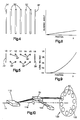
- an ion implantation system 10 having an ion source 12 for directing an ion beam 14 along a trajectory leading to an ion mass analyzing magnet 16.
- the magnet 16 bends the beam at approximately a right angle and directs ions having an appropriate mass along a travel path through a resolving aperture 20.
- the shutter 20 rejects ions having an inappropriate mass from the ion beam.
- the beam 14 then passes through a pair of deflection electrodes 26, 28.
- Control voltages applied to the electrodes 26, 28 by a control circuit 29 cause the ion beam to pass through electric fields which deflect the ion beam 14 by a controlled amount.
- the magnitude of the voltage difference between the two plates 26, 28 controls the amount of deflection.
- the deflected ion beam enters an electrostatic lens 30 where it is redirected along a travel path generally parallel to the trajectory the beam follows as it exits the analyzing magnet 16.
- the electrostatic lens 30 includes a number of individual electrodes 32 and a pair of spaced parallel plates 34, 36 ( Figure 2). After passing through the lens 30 the ions in the beam are optionally accelerated to a final implantation energy by an electrostatic accelerator 38.
- an ion implantation station 40 Downstream from the electrostatic lens 30, an ion implantation station 40 includes structure that supports a semiconductor wafer at a position to intercept ions that have been accelerated by accelerator 38. Ion beam collisions with other particles degrade beam integrity so that the entire beam line from the source 12 to the implantation station 40 is evacuated. At the region of the ion implantation station 40 a chamber 42 is evacuated and the wafers are inserted into and withdrawn from load locks to avoid repeated pressurization and depressurization of the chamber 42.
- a mechanized arm 44 grasps wafers retrieved from a cassette 50 by a shuttle 52 and positions each undoped wafer on a wafer orienter 56.
- the orienter 56 rotates the undoped wafer to a particular orientation before ion implantation so that as ions strike the wafer they encounter a specific orientation of the crystal lattice structure.
- the wafer is then moved into a load lock 58 so that a second arm 46 can move the wafers to an implant position within the chamber 42.
- a wafer support 59 orients the wafer 60 with respect to the ion beam at a specific tilt angle that remains constant due to the parallel ion beam orientation.
- the scanning electrodes 26, 28 produce side-to-side beam scanning of a controlled amount under the direction of the control circuitry 29.
- the circuitry includes a programmable controller for adjusting the scanning electrode voltages to achieve this wafer scanning.
- the particular system depicted in Figure 1 produces only side-to-side scanning so that to fully implant a workpiece such as the circular wafers depicted in Figure 1, an additional relative motion between the deflected ion beam and the workpiece is necessary.
- a linear back and forth scan of a wafer 60 at the ion implantation station 40 is achieved through suitable drive mechanisms (not shown) for the support 59.
- the now-doped wafer is removed from the implantation station 40 by a third arm 62.
- This arm 62 delivers the wafer 60 to a load lock 64 so that a fourth mechanized arm 66 can transfer the wafer to a shuttle 68 that stores the doped wafer in a cassette 70.
- Figures 2 and 3 illustrate one of two disclosed lens configurations. Individual ions from the beam 14 are deflected by the voltages of the two metal plates 26, 28 and pass through a region bounded by the two plates 34, 36 and a plurality of metal electrodes 32. The spacing between the two plates 34, 36 define the width of the electrostatic lens 30. As depicted in the graph of Figure 7, the plate 34 is maintained at a constant electric potential less than the potential on the plate 36 by a power supply 37. In Figures 6 and 7 the abscissa "x" designates a distance from the plate 34. The voltages on the electrodes 32 depend upon the relative positioning of those electrodes with respect to the two plates 34, 36. The electrode voltages increase from the plate 34 to the plate 36.
- the voltage on the electrodes is chosen to vary linearly with the position between the two plates 34, 36 and is maintained by a suitably constructed direct current power supply capable of providing a voltage difference between the plates 34, 36 of hundreds of volts.
- the plate 34 is shorter than the plate 36 and the electrode length also varies.
- the dimensions of the electrodes and plates and the choice of biasing voltages applied to the electrodes and plates produce a bending angle depicted in Figure 6. Those ions that are deflected the greatest amount by the plates 26, 28 are redeflected a greater amount due to longer electrostatic interaction with the electric fields created within the lens.
- the position at which ions enter the region between the two plates 34, 36 varies with the initial deflection angle. Due to the compensating effect of the lens 30 a proportional redefection occurs and all ions entering the lens exit along parallel paths. By controlled side to side beam deflection a narrow uniform ion beam that traverses the entire width of the wafer 60 is provided.
- FIGs 4 and 5 depict an alternative arrangement for an electrostatic lens 30'.
- both plates 34', 36' and all electrodes 32' have the same length.
- the electrodes and plates are each held at a respective constant voltage but as seen in Figure 9, the voltage variation between the two plates is nonlinear. The net result is a bending angle which is linear with respect to position (see Figure 8).
- the curve depicted in Figure 9 is of the form V a ⁇ X m where m is approximately two and X is the distance from the electrode 34'.
- V a is proportional to the beam energy and the incoming scan angle as well as the dimensions, number and spacing of the electrodes.
- Figure 11 an enlarged view of the Figure 4 depiction is disclosed to show the electric field lines in the vicinity of the electrodes 32' and end plates 34', 36'.
- the lens has a total width of 240 mm with equal spacing between electrodes.
- the electrode length is approximately 8 inches.
- the voltage on each electrode is adjusted for each relevant parameter and then fixed for a particular ion implantation. Although the voltages vary for different parameters the ratio of the voltages should conform to the proportionality given above.
- the wafer is mounted to a support 59 which traverses back and forth through the thin, generally planar ion beam. This avoids the need for a large lens opening with accompanying loss of precise control of the electric field.
- Figure 10 depicts an alternative arrangement in which the electrostatic lens 30 is mounted to a elongated support 100 which rotates about an axis 110 corresponding to an initial beam trajectory.
- Ions within the beam 14 enter a deflection station 112 that includes a pair of parallel deflection plates mounted for rotation.
- the ion beam is deflected a variable amount and scanned about the rotation axis 110.
- Rotation of the scanning electrodes and electrostatic lens is simultaneous and preferably accomplished by a mechanical interconnection of the scanning plates and lens. This allows a single motor to rotate both the deflection plates and the lens 30.
- the scanning plates deflect the ion beam, the ions pass through the electrostatic lens 30 and are redeflected along parallel paths to an ion implantation station 120.
- a wafer support 122 carries plurality of semiconductor wafers 60.
- the wafer support 122 is mounted for movement between a position in which the wafers are placed onto the support and a second position in which the wafers are presented for implantation.
- the wafers remain stationary as the deflecting plate and electrostatic lens are rotated causing the parallel rays from the ion beam to impact the circularly arranged semiconductor wafers 60.
- a slightly different embodiment of the structure depicted in Figure 10 would include fixed deflection plates and electrostatic lens and a rotating wafer support for causing multiple wafers to pass through the parallel rays of the twice deflected ion beam.
- the control electronics 29 coupled to the deflection plates 26, 28 is necessary to assure uniform ion implantation.
- Such electronics is typically coupled to a programmable controller which automatically applies a variable voltage signal across the two parallel plates causing the angle at which the ion beam is deflected to vary with time.
- a cyclic beam deflection is provided causing a uniform ion implantation dosage as relative rotation between the ion beam and wafers is provided.
Description
- The present invention concerns an ion implanter for treating workpieces and has a particular application in ion implanting semiconductor wafers.
- It is known in the semiconductor fabrication art to use an ion beam to dope semiconductor wafers with ion impurities. By scanning a beam across a wafer surface or moving the wafer through a stationary beam the wafer can be uniformly doped.
- The angle at which an ion beam impacts a wafer surface (wafer tilt) is an important parameter in ion implantation of the wafer. Recent trends in semiconductor material processing require a decreased ion impact angle variation across the wafer surface.
- In a scanning ion beam system, electrostatic deflection plates produce a raster pattern of ion beam impingement on the wafer surface. One set of plates produces a rapid back and forth scan in one direction and a second set of plates provides beam deflection in an orthogonal direction. Such raster scanning results in impact angle variations of ±4° across a 200 mm wafer for a typical ion beam geometry.
- Methods have been proposed to reduce this impact angle variation. One proposal suggests using four sets of deflection plates, two horizontal and two vertical, and is referred to as a double deflection system. The beam is first deflected away from an initial trajectory and then, just before striking the wafer, is deflected again to return to a direction parallel to its original, undeflected trajectory.
- Use of a double deflection system with large wafer diameters requires deflection plates that are more widely spaced. This requires high deflection voltages that must be scanned and precisely synchronized with the scanning voltages applied to the first set of deflection plates. Another problem is that as the opening in the scan plates increases, electrostatic fringing fields become more difficult to control and become more susceptible to beam space charge effects.
- Another known method of reducing tilt variations is to use a mechanically scanned, spinning disk wafer support. If the spin axis is parallel to the beam, no impact angle variations are present. Spinning disk supports have problems achieving control over impact angle while maintaining the necessary condition for an impact angle variation. One example of a prior art patent having a spinning workpiece support is U.S. patent 4,794,305 to Matsukawa.
- Another more recent approach is to electrostatically scan the beam in one axis, and then use a highly indexed bending magnet to produce a parallel ribbon beam. The wafer is then scanned mechanically in a direction orthogonal to the ribbon beam to produce a uniform two dimensional implant. U.S. patents 4,276,477 to Enge, 4,687,936 to McIntyre et al. and 4,922,106 to Berrian et al. (corresponding to WO 87/06391) disclose such systems.
- In one aspect the invention, as defined by claim 1, provides an ion beam implant system for controllably treating a workpiece, the system comprising: source means for providing ions to treat the workpiece; support means for orienting the workpiece at a location relative the source means; beam forming means for causing ions emitted by the source means to form an ion beam moving in a first trajectory; deflection means for deflecting ions in said ion beam away from said first trajectory by controlled initial deflection amounts along diverging trajectories; control means having an output coupled to said deflection means to adjust the deflecting of said ion beam and thereby control treatment of the workpiece; and lens means for directing the ions deflected by said deflection means to impact trajectories that intercept said workpiece at a uniform, controlled impact angle; characterized: in that said lens means comprises a plurality of electrodes bounding the ion beam travel path for setting up a non-uniform static electric field to intercept and redeflect the ions moving along said diverging trajectories; and by biasing means for controlling respective voltages on the plurality of electrodes so that a strength of the non-uniform static electric field varies across said ion beam travel path in relation to a degree of divergence of the ions in the ion beam from the first trajectory whereby the redeflected ions are directed to said impact trajectories.
- The preamble of claim 1 reflects the state of the art according to U.S. patent 4,611,712 to Mobley (corresponding to WO 86/07189), which discloses an apparatus for scanning an ion beam over the surface of a workpiece while maintaining a substantially constant angle of incidence, the apparatus having a beam deflection system followed by a space charge lens.
- In accordance with the ion beam implant system of the invention, the lens means has a plurality of lens electrodes arranged in spaced relation to the ion beam travel path and biased to specified control voltages. The resultant electric field created by the voltages of the lens electrodes bends the ion beam by an amount dependent upon the travel path of the ion beam through the electrostatic lens as well as the mass and energy of the ions. The operation of the lens is analogous to the operation of an optical lens since the amount of deflection the ion beam experiences varies with the angle and position at which the ion beam enters the electric field generated by the lens.
- In accordance with a preferred embodiment of the invention, the controlled initial deflection and redirection due to operation of the electrostatic lens is accomplished in one dimension. Two-dimensional scanning of a workpiece is accomplished by relative movement of the scanning structure in relation to the workpiece. This can be accomplished by either movement of the workpiece or movement of the beam deflecting structure. An alternative to this preferred design uses a circular scanning motion wherein the deflecting or scanning electrode as well as the electrostatic lens structure is rotated at a controlled rate as the deflected ion beam impacts a circular array of stationary wafers.
- In another aspect the invention provides the electrostatic lens defined by claim 6.
- In a further aspect the invention provides the method defined by claim 8 for implanting a workpiece with an ion beam.
-
- Figure 1 is a schematic of an ion implantation system constructed in accordance with the invention;
- Figure 2 is a plan view of an electrostatic lens structure for deflecting an ion beam as it passes to the region of a workpiece;
- Figure 3 is an elevation view of the Figure 2 electrostatic lens;
- Figure 4 is a plan view of an alternative embodiment of an electrostatic lens structure constructed in accordance with the invention;
- Figure 5 is an elevation view of the Figure 4 electrostatic lens;
- Figure 6 is a graph of bending angle vs. position for the lens structure of Figure 2;
- Figure 7 is a graph of electrode voltage vs. position for the lens structure of Figure 2;
- Figure 8 is a graph of bending angle vs. position for the Figure 4 electrostatic lens;
- Figure 9 is a graph of electrode voltage vs. position for the Figure 4 electrostatic lens;
- Figure 10 is a schematic showing a circular scanning ion beam implanter for implanting a plurality of workpieces; and
- Figure 11 is an enlarged view of the Figure 5 depiction showing electric field lines created due to application of control voltages to the electrodes of the electrostatic lens.
- Turning now to the drawings, an
ion implantation system 10 is illustrated having anion source 12 for directing anion beam 14 along a trajectory leading to an ionmass analyzing magnet 16. Themagnet 16 bends the beam at approximately a right angle and directs ions having an appropriate mass along a travel path through aresolving aperture 20. Theshutter 20 rejects ions having an inappropriate mass from the ion beam. - The
beam 14 then passes through a pair ofdeflection electrodes electrodes control circuit 29 cause the ion beam to pass through electric fields which deflect theion beam 14 by a controlled amount. The magnitude of the voltage difference between the twoplates electrostatic lens 30 where it is redirected along a travel path generally parallel to the trajectory the beam follows as it exits the analyzingmagnet 16. Theelectrostatic lens 30 includes a number ofindividual electrodes 32 and a pair of spacedparallel plates 34, 36 (Figure 2). After passing through thelens 30 the ions in the beam are optionally accelerated to a final implantation energy by anelectrostatic accelerator 38. - Downstream from the
electrostatic lens 30, anion implantation station 40 includes structure that supports a semiconductor wafer at a position to intercept ions that have been accelerated byaccelerator 38. Ion beam collisions with other particles degrade beam integrity so that the entire beam line from thesource 12 to theimplantation station 40 is evacuated. At the region of the ion implantation station 40 achamber 42 is evacuated and the wafers are inserted into and withdrawn from load locks to avoid repeated pressurization and depressurization of thechamber 42. A mechanizedarm 44 grasps wafers retrieved from acassette 50 by ashuttle 52 and positions each undoped wafer on awafer orienter 56. The orienter 56 rotates the undoped wafer to a particular orientation before ion implantation so that as ions strike the wafer they encounter a specific orientation of the crystal lattice structure. The wafer is then moved into aload lock 58 so that asecond arm 46 can move the wafers to an implant position within thechamber 42. At the implantation site awafer support 59 orients thewafer 60 with respect to the ion beam at a specific tilt angle that remains constant due to the parallel ion beam orientation. - The
scanning electrodes control circuitry 29. The circuitry includes a programmable controller for adjusting the scanning electrode voltages to achieve this wafer scanning. The particular system depicted in Figure 1 produces only side-to-side scanning so that to fully implant a workpiece such as the circular wafers depicted in Figure 1, an additional relative motion between the deflected ion beam and the workpiece is necessary. In this implementation, a linear back and forth scan of awafer 60 at theion implantation station 40 is achieved through suitable drive mechanisms (not shown) for thesupport 59. - Once the
wafer 60 has been doped by treatment with the ion beam, the now-doped wafer is removed from theimplantation station 40 by athird arm 62. Thisarm 62 delivers thewafer 60 to aload lock 64 so that a fourthmechanized arm 66 can transfer the wafer to ashuttle 68 that stores the doped wafer in acassette 70. - Figures 2 and 3 illustrate one of two disclosed lens configurations. Individual ions from the
beam 14 are deflected by the voltages of the twometal plates plates metal electrodes 32. The spacing between the twoplates electrostatic lens 30. As depicted in the graph of Figure 7, theplate 34 is maintained at a constant electric potential less than the potential on theplate 36 by apower supply 37. In Figures 6 and 7 the abscissa "x" designates a distance from theplate 34. The voltages on theelectrodes 32 depend upon the relative positioning of those electrodes with respect to the twoplates plate 34 to theplate 36. - Generally, the voltage on the electrodes is chosen to vary linearly with the position between the two
plates plates - As seen in Figure 2, the
plate 34 is shorter than theplate 36 and the electrode length also varies. The dimensions of the electrodes and plates and the choice of biasing voltages applied to the electrodes and plates produce a bending angle depicted in Figure 6. Those ions that are deflected the greatest amount by theplates - The position at which ions enter the region between the two
plates wafer 60 is provided. - Figures 4 and 5 depict an alternative arrangement for an electrostatic lens 30'. In this arrangement, both plates 34', 36' and all electrodes 32' have the same length. The electrodes and plates are each held at a respective constant voltage but as seen in Figure 9, the voltage variation between the two plates is nonlinear. The net result is a bending angle which is linear with respect to position (see Figure 8).
- The curve depicted in Figure 9 is of the form Va α Xm where m is approximately two and X is the distance from the electrode 34'. Va is proportional to the beam energy and the incoming scan angle as well as the dimensions, number and spacing of the electrodes. In Figure 11 an enlarged view of the Figure 4 depiction is disclosed to show the electric field lines in the vicinity of the electrodes 32' and end plates 34', 36'.
- In the Figure 11 depiction the lens has a total width of 240 mm with equal spacing between electrodes. The electrode length is approximately 8 inches. The voltage on each electrode is adjusted for each relevant parameter and then fixed for a particular ion implantation. Although the voltages vary for different parameters the ratio of the voltages should conform to the proportionality given above.
- It is possible to adjust the value of the exponent m to tune the ion beam's degree of parallelism and to adjust for fringing field effects at the entrance and exit of the lens. Values of m from 1.8 to 2.2 have been used and the resulting voltages are tabulated below in Table 1.

- As noted above, in the Figure 1 embodiment of the invention, the wafer is mounted to a
support 59 which traverses back and forth through the thin, generally planar ion beam. This avoids the need for a large lens opening with accompanying loss of precise control of the electric field. - Figure 10 depicts an alternative arrangement in which the
electrostatic lens 30 is mounted to aelongated support 100 which rotates about anaxis 110 corresponding to an initial beam trajectory. Ions within thebeam 14 enter adeflection station 112 that includes a pair of parallel deflection plates mounted for rotation. The ion beam is deflected a variable amount and scanned about therotation axis 110. Rotation of the scanning electrodes and electrostatic lens is simultaneous and preferably accomplished by a mechanical interconnection of the scanning plates and lens. This allows a single motor to rotate both the deflection plates and thelens 30. As the scanning plates deflect the ion beam, the ions pass through theelectrostatic lens 30 and are redeflected along parallel paths to anion implantation station 120. At this ion implantation station awafer support 122 carries plurality ofsemiconductor wafers 60. - The
wafer support 122 is mounted for movement between a position in which the wafers are placed onto the support and a second position in which the wafers are presented for implantation. The wafers remain stationary as the deflecting plate and electrostatic lens are rotated causing the parallel rays from the ion beam to impact the circularly arrangedsemiconductor wafers 60. - A slightly different embodiment of the structure depicted in Figure 10 would include fixed deflection plates and electrostatic lens and a rotating wafer support for causing multiple wafers to pass through the parallel rays of the twice deflected ion beam.
- The
control electronics 29 coupled to thedeflection plates - The invention has been described in conjunction with multiple alternate embodiments. It is the intent that the invention include all modifications and alterations from these embodiments falling within the scope of the appended claims.
Claims (8)
- An ion beam implant system for controllably treating a workpiece (60), the system comprising:source means (12) for providing ions to treat the workpiece;support means (59;122) for orienting the workpiece at a location relative the source means;beam forming means (16,20) for causing ions emitted by the source means to form an ion beam (14) moving in a first trajectory;deflection means (26,28; 112) for deflecting ions in said ion beam away from said first trajectory by controlled initial deflection amounts along diverging trajectories;control means (29) having an output coupled to said deflection means to adjust the deflecting of said ion beam and thereby control treatment of the workpiece; andlens means (30) for directing the ions deflected by said deflection means to impact trajectories that intercept said workpiece at a uniform, controlled impact angle, said lens means comprising electrode means (32) and biasing means (37) for controlling the voltage on said electrode means;characterized in that:said electrode means comprises a plurality of electrodes (32) bounding the ion beam travel path for setting up a non-uniform static electric field to intercept and redeflect the ions moving along said diverging trajectories; andsaid biasing means (37) controls respective voltages on the plurality of electrodes so that the strength of the non-uniform static electric field varies across said ion beam travel path in relation to the degree of divergence of the ions in the ion beam from the first trajectory whereby the redeflected ions are directed to said impact trajectories.
- An ion beam implant system according to claim 1, wherein said deflection means (112) and said lens means (30) are mechanically interconnected and further comprising means to rotate said deflection means and lens means about an axis (110) to sweep over a scanned workpiece.
- An ion beam implant system according to claim 1, wherein said deflection means (26,28) and said lens means (30) are fixed and the support means (59) moves the workpiece relative the ion beam.
- An ion beam implant system according to any of claims 1 to 3, wherein said plurality of electrodes (32) are elongate and positioned in spaced relationship to define two rows of electrodes bounding opposite sides of a region through which the ions pass and are redeflected.
- An ion beam implant system according to claim 4, wherein said lens means (30) includes first and second conductive plates (34,36) spanning a gap between said two rows of electrodes, said biasing means (37) applying voltages to said first and second conductive plates and said plurality of electrodes to set up the non-uniform static electric field.
- An electrostatic lens for an ion beam implant system, the implant system deflecting the ions in said ion beam away from its first trajectory along diverging trajectories and the lens providing an ion deflection region in which the diverging ions are further deflected to impact trajectories on their way to a target, the lens comprising:a plurality of elongate conductive electrodes (32) spaced from each other to define a first row of electrodes bounding one side of said region;a plurality of elongate conductive electrodes (32) spaced from each other to define a second row of electrodes bounding an opposing side of said region;first and second conductive plates (34,36) spanning a gap between said first and second rows of electrodes and which combine with said first and second rows of electrodes to define the ion deflection region through which ions pass and are deflected before striking the target; andbiasing means (37) for applying respective voltages to the electrodes of the first and second rows and to the first and second conductive plates to produce a static non-uniform electric field within the deflection region, so that the strength of the non-uniform electric field varies across the ion beam travel path in relation to the degree of divergence of the ions in the ion beam from the first trajectory whereby the redeflected ions are directed to said impact trajectories.
- An electrostatic lens according to claim 6, wherein the biasing means (37) applies voltages to the electrodes (32) and the first and second conductive plates (34,36) to create an electric field tending to cause the ions to exit the deflection region with approximately parallel trajectories.
- A method for implanting a workpiece with an ion beam, the method comprising:providing an ion beam having ions that move along a first trajectory; deflecting ions from the first trajectory by controlled amounts to create a diverging ion beam;creating a non-uniform static electric field at a region for intercepting the diverging ion beam and which redeflects the ions in the diverging ion beam to workpiece impact trajectories that are generally parallel to each other, by controlling respective voltages on a plurality of electrodes bounding said region so that the strength of the non-uniform static electric field varies across said region in relation to the degree of divergence of the ions in the ion beam from the first trajectory; andproviding relative scanning movement between the workpiece and the ion beam subsequent to said region where the ion beam is redeflected.
Applications Claiming Priority (2)
| Application Number | Priority Date | Filing Date | Title |
|---|---|---|---|
| US59236390A | 1990-10-03 | 1990-10-03 | |
| US592363 | 1990-10-03 |
Publications (3)
| Publication Number | Publication Date |
|---|---|
| EP0486149A2 EP0486149A2 (en) | 1992-05-20 |
| EP0486149A3 EP0486149A3 (en) | 1992-06-10 |
| EP0486149B1 true EP0486149B1 (en) | 1996-12-18 |
Family
ID=24370360
Family Applications (1)
| Application Number | Title | Priority Date | Filing Date |
|---|---|---|---|
| EP91309036A Expired - Lifetime EP0486149B1 (en) | 1990-10-03 | 1991-10-02 | Method and apparatus for reducing tilt angle variations in an ion implanter |
Country Status (4)
| Country | Link |
|---|---|
| EP (1) | EP0486149B1 (en) |
| JP (1) | JP3106214B2 (en) |
| KR (1) | KR970002681B1 (en) |
| DE (1) | DE69123708T2 (en) |
Families Citing this family (6)
| Publication number | Priority date | Publication date | Assignee | Title |
|---|---|---|---|---|
| US7005657B1 (en) | 2005-02-04 | 2006-02-28 | Varian Semiconductor Equipment Associates, Inc. | Wafer-scanning ion implanter having fast beam deflection apparatus for beam glitch recovery |
| US7361913B2 (en) * | 2005-04-02 | 2008-04-22 | Varian Semiconductor Equipment Associates, Inc. | Methods and apparatus for glitch recovery in stationary-beam ion implantation process using fast ion beam control |
| KR100675891B1 (en) * | 2005-05-04 | 2007-02-02 | 주식회사 하이닉스반도체 | Apparatus and method of implanting ions partially |
| US7696494B2 (en) | 2006-06-12 | 2010-04-13 | Axcelis Technologies, Inc. | Beam angle adjustment in ion implanters |
| JP5338022B2 (en) * | 2006-07-12 | 2013-11-13 | 富士通株式会社 | Irradiation direction variable ion irradiation apparatus and secondary ion mass spectrometer |
| KR101148131B1 (en) * | 2010-11-01 | 2012-05-23 | 부산교통공사 | Apparatus for injecting grease into a axle bearing of railcar |
Family Cites Families (4)
| Publication number | Priority date | Publication date | Assignee | Title |
|---|---|---|---|---|
| US4556823A (en) * | 1983-07-28 | 1985-12-03 | International Business Machines Corporation | Multi-function charged particle apparatus |
| US4661712A (en) * | 1985-05-28 | 1987-04-28 | Varian Associates, Inc. | Apparatus for scanning a high current ion beam with a constant angle of incidence |
| WO1987006391A1 (en) * | 1986-04-09 | 1987-10-22 | Eclipse Ion Technology, Inc. | Ion beam scanning method and apparatus |
| EP0344513A3 (en) * | 1988-05-31 | 1991-01-16 | Siemens Aktiengesellschaft | Process for the manufacture of a steering plate for a lithography apparatus |
-
1991
- 1991-10-01 KR KR1019910017170A patent/KR970002681B1/en not_active IP Right Cessation
- 1991-10-02 JP JP03282061A patent/JP3106214B2/en not_active Expired - Fee Related
- 1991-10-02 DE DE69123708T patent/DE69123708T2/en not_active Expired - Fee Related
- 1991-10-02 EP EP91309036A patent/EP0486149B1/en not_active Expired - Lifetime
Also Published As
| Publication number | Publication date |
|---|---|
| DE69123708T2 (en) | 1997-07-10 |
| KR920008846A (en) | 1992-05-28 |
| EP0486149A3 (en) | 1992-06-10 |
| DE69123708D1 (en) | 1997-01-30 |
| EP0486149A2 (en) | 1992-05-20 |
| JPH04280054A (en) | 1992-10-06 |
| KR970002681B1 (en) | 1997-03-08 |
| JP3106214B2 (en) | 2000-11-06 |
Similar Documents
| Publication | Publication Date | Title |
|---|---|---|
| US5160846A (en) | Method and apparatus for reducing tilt angle variations in an ion implanter | |
| US5091655A (en) | Reduced path ion beam implanter | |
| US4276477A (en) | Focusing apparatus for uniform application of charged particle beam | |
| EP1774559B1 (en) | Electrostatic lens for ion beams | |
| EP0559359B1 (en) | Ion beam implanter for providing cross plane focusing | |
| JP3730666B2 (en) | Large current ribbon beam injector | |
| US7982195B2 (en) | Controlled dose ion implantation | |
| US7902527B2 (en) | Apparatus and methods for ion beam implantation using ribbon and spot beams | |
| CN1256751C (en) | High efficiency scanning in ion implanters | |
| US6777695B2 (en) | Rotating beam ion implanter | |
| KR20060135908A (en) | Method and fine-control collimator for accurate collimation and precise parallel alignment of scanned ion beams | |
| US5373164A (en) | Ion beam conical scanning system | |
| JP2008503067A (en) | Ion beam scanning system and method for improved ion implantation homogenization | |
| US6207963B1 (en) | Ion beam implantation using conical magnetic scanning | |
| US6774377B1 (en) | Electrostatic parallelizing lens for ion beams | |
| KR20160134649A (en) | Ion implantation system and method with variable energy control | |
| EP0377298B1 (en) | Uniform cross section ion beam system | |
| EP0486149B1 (en) | Method and apparatus for reducing tilt angle variations in an ion implanter |
Legal Events
| Date | Code | Title | Description |
|---|---|---|---|
| PUAI | Public reference made under article 153(3) epc to a published international application that has entered the european phase |
Free format text: ORIGINAL CODE: 0009012 |
|
| PUAL | Search report despatched |
Free format text: ORIGINAL CODE: 0009013 |
|
| AK | Designated contracting states |
Kind code of ref document: A2 Designated state(s): DE FR GB |
|
| AK | Designated contracting states |
Kind code of ref document: A3 Designated state(s): DE FR GB |
|
| 17P | Request for examination filed |
Effective date: 19921123 |
|
| 17Q | First examination report despatched |
Effective date: 19941212 |
|
| GRAG | Despatch of communication of intention to grant |
Free format text: ORIGINAL CODE: EPIDOS AGRA |
|
| GRAH | Despatch of communication of intention to grant a patent |
Free format text: ORIGINAL CODE: EPIDOS IGRA |
|
| GRAH | Despatch of communication of intention to grant a patent |
Free format text: ORIGINAL CODE: EPIDOS IGRA |
|
| GRAA | (expected) grant |
Free format text: ORIGINAL CODE: 0009210 |
|
| AK | Designated contracting states |
Kind code of ref document: B1 Designated state(s): DE FR GB |
|
| REF | Corresponds to: |
Ref document number: 69123708 Country of ref document: DE Date of ref document: 19970130 |
|
| ET | Fr: translation filed | ||
| PGFP | Annual fee paid to national office [announced via postgrant information from national office to epo] |
Ref country code: FR Payment date: 19971007 Year of fee payment: 7 |
|
| PLBE | No opposition filed within time limit |
Free format text: ORIGINAL CODE: 0009261 |
|
| STAA | Information on the status of an ep patent application or granted ep patent |
Free format text: STATUS: NO OPPOSITION FILED WITHIN TIME LIMIT |
|
| 26N | No opposition filed | ||
| PGFP | Annual fee paid to national office [announced via postgrant information from national office to epo] |
Ref country code: DE Payment date: 19981028 Year of fee payment: 8 |
|
| PG25 | Lapsed in a contracting state [announced via postgrant information from national office to epo] |
Ref country code: FR Free format text: LAPSE BECAUSE OF NON-PAYMENT OF DUE FEES Effective date: 19990630 |
|
| REG | Reference to a national code |
Ref country code: FR Ref legal event code: ST |
|
| PG25 | Lapsed in a contracting state [announced via postgrant information from national office to epo] |
Ref country code: DE Free format text: LAPSE BECAUSE OF NON-PAYMENT OF DUE FEES Effective date: 20000801 |
|
| REG | Reference to a national code |
Ref country code: GB Ref legal event code: 732E |
|
| REG | Reference to a national code |
Ref country code: GB Ref legal event code: IF02 |
|
| PGFP | Annual fee paid to national office [announced via postgrant information from national office to epo] |
Ref country code: GB Payment date: 20060915 Year of fee payment: 16 |
|
| GBPC | Gb: european patent ceased through non-payment of renewal fee |
Effective date: 20071002 |
|
| PG25 | Lapsed in a contracting state [announced via postgrant information from national office to epo] |
Ref country code: GB Free format text: LAPSE BECAUSE OF NON-PAYMENT OF DUE FEES Effective date: 20071002 |