EP0484263A1 - Transition metal-compound dopant source and semiconductor device contact - Google Patents
Transition metal-compound dopant source and semiconductor device contact Download PDFInfo
- Publication number
- EP0484263A1 EP0484263A1 EP91480160A EP91480160A EP0484263A1 EP 0484263 A1 EP0484263 A1 EP 0484263A1 EP 91480160 A EP91480160 A EP 91480160A EP 91480160 A EP91480160 A EP 91480160A EP 0484263 A1 EP0484263 A1 EP 0484263A1
- Authority
- EP
- European Patent Office
- Prior art keywords
- layer
- region
- transition metal
- substrate
- accordance
- Prior art date
- Legal status (The legal status is an assumption and is not a legal conclusion. Google has not performed a legal analysis and makes no representation as to the accuracy of the status listed.)
- Withdrawn
Links
Images


Classifications
-
- H—ELECTRICITY
- H10—SEMICONDUCTOR DEVICES; ELECTRIC SOLID-STATE DEVICES NOT OTHERWISE PROVIDED FOR
- H10W—GENERIC PACKAGES, INTERCONNECTIONS, CONNECTORS OR OTHER CONSTRUCTIONAL DETAILS OF DEVICES COVERED BY CLASS H10
- H10W20/00—Interconnections in chips, wafers or substrates
- H10W20/01—Manufacture or treatment
- H10W20/031—Manufacture or treatment of conductive parts of the interconnections
- H10W20/069—Manufacture or treatment of conductive parts of the interconnections by forming self-aligned vias or self-aligned contact plugs
-
- H—ELECTRICITY
- H10—SEMICONDUCTOR DEVICES; ELECTRIC SOLID-STATE DEVICES NOT OTHERWISE PROVIDED FOR
- H10D—INORGANIC ELECTRIC SEMICONDUCTOR DEVICES
- H10D10/00—Bipolar junction transistors [BJT]
- H10D10/01—Manufacture or treatment
- H10D10/051—Manufacture or treatment of vertical BJTs
-
- H—ELECTRICITY
- H10—SEMICONDUCTOR DEVICES; ELECTRIC SOLID-STATE DEVICES NOT OTHERWISE PROVIDED FOR
- H10P—GENERIC PROCESSES OR APPARATUS FOR THE MANUFACTURE OR TREATMENT OF DEVICES COVERED BY CLASS H10
- H10P14/00—Formation of materials, e.g. in the shape of layers or pillars
- H10P14/40—Formation of materials, e.g. in the shape of layers or pillars of conductive or resistive materials
- H10P14/418—Formation of materials, e.g. in the shape of layers or pillars of conductive or resistive materials the conductive layers comprising transition metals
-
- H—ELECTRICITY
- H10—SEMICONDUCTOR DEVICES; ELECTRIC SOLID-STATE DEVICES NOT OTHERWISE PROVIDED FOR
- H10P—GENERIC PROCESSES OR APPARATUS FOR THE MANUFACTURE OR TREATMENT OF DEVICES COVERED BY CLASS H10
- H10P32/00—Diffusion of dopants within, into or out of wafers, substrates or parts of devices
- H10P32/10—Diffusion of dopants within, into or out of semiconductor bodies or layers
- H10P32/14—Diffusion of dopants within, into or out of semiconductor bodies or layers within a single semiconductor body or layer in a solid phase; between different semiconductor bodies or layers, both in a solid phase
- H10P32/1408—Diffusion of dopants within, into or out of semiconductor bodies or layers within a single semiconductor body or layer in a solid phase; between different semiconductor bodies or layers, both in a solid phase from or through or into an external applied layer, e.g. photoresist or nitride layers
-
- H—ELECTRICITY
- H10—SEMICONDUCTOR DEVICES; ELECTRIC SOLID-STATE DEVICES NOT OTHERWISE PROVIDED FOR
- H10P—GENERIC PROCESSES OR APPARATUS FOR THE MANUFACTURE OR TREATMENT OF DEVICES COVERED BY CLASS H10
- H10P32/00—Diffusion of dopants within, into or out of wafers, substrates or parts of devices
- H10P32/10—Diffusion of dopants within, into or out of semiconductor bodies or layers
- H10P32/17—Diffusion of dopants within, into or out of semiconductor bodies or layers characterised by the semiconductor material
- H10P32/171—Diffusion of dopants within, into or out of semiconductor bodies or layers characterised by the semiconductor material being group IV material
-
- Y—GENERAL TAGGING OF NEW TECHNOLOGICAL DEVELOPMENTS; GENERAL TAGGING OF CROSS-SECTIONAL TECHNOLOGIES SPANNING OVER SEVERAL SECTIONS OF THE IPC; TECHNICAL SUBJECTS COVERED BY FORMER USPC CROSS-REFERENCE ART COLLECTIONS [XRACs] AND DIGESTS
- Y10—TECHNICAL SUBJECTS COVERED BY FORMER USPC
- Y10S—TECHNICAL SUBJECTS COVERED BY FORMER USPC CROSS-REFERENCE ART COLLECTIONS [XRACs] AND DIGESTS
- Y10S148/00—Metal treatment
- Y10S148/034—Diffusion of boron or silicon
-
- Y—GENERAL TAGGING OF NEW TECHNOLOGICAL DEVELOPMENTS; GENERAL TAGGING OF CROSS-SECTIONAL TECHNOLOGIES SPANNING OVER SEVERAL SECTIONS OF THE IPC; TECHNICAL SUBJECTS COVERED BY FORMER USPC CROSS-REFERENCE ART COLLECTIONS [XRACs] AND DIGESTS
- Y10—TECHNICAL SUBJECTS COVERED BY FORMER USPC
- Y10S—TECHNICAL SUBJECTS COVERED BY FORMER USPC CROSS-REFERENCE ART COLLECTIONS [XRACs] AND DIGESTS
- Y10S148/00—Metal treatment
- Y10S148/035—Diffusion through a layer
Definitions
- the present invention relates generally to semiconductor devices and more particularly to the use of a transition metal-compound as a self-aligned diffusion source and electrical contact to a doped semiconductor region.
- U.S. patent 4,490,193 to Ishaq et al. shows a method of making a diffusion into a semiconductor substrate, using a rare earth boride dopant source, wherein the rare earth boride material remains as an ohmic electrical contact to the doped region.
- U.S. patent 4,481,046 to Bouldin et al. also assigned to the assignee of the present invention, is similar to Ihaq et al. in that the latter teaches the use of a rare earth hexaboride material, containing a predetermined amount of silicon, for the same purposes.
- These rare earth boride/hexaboride materials suffer from the disadvantage of reacting with silicon at temperatures in the 1,000 + _C range. Such a reaction can damage the underlying silicon region or devices contained therein.
- TiN titanium nitride
- TiSi2 titanium silicide
- U.S. patent 4,734,386 shows the use of chemical vapor-phase deposited boron nitride as a solid dopant source for diffusion doping of semiconductor substrates.
- An object of the present invention is to provide a new and improved method and structure for both solid phase doping and providing an electrical contact to a thusly doped semiconductor region.
- Another object of the present invention is to provide such a dopant source/contact having low electrical resistance.
- Yet another object of the present invention is to provide such a dopant source/contact having etch characteristics different from silicon so that the dopant source/contact can be etched selectively to silicon.
- a further object of the present invention is to provide such a dopant source/contact which is compatible with associated transistor structures.
- Yet a further object of the present invention is to provide such a dopant source/contact which does not react with silicon at conventional semiconductor processing temperatures.
- a new and improved method of forming a self-aligned contact to a doped region on a semiconductor substrate comprising the steps of: providing a substrate of semiconductor material; forming a first layer of a transition metal-boride compound over at least one selected portion of the substrate; forming a second layer of a transition metal-nitride compound over the first layer; and heating to drive dopant from the first layer into the substrate.
- an electrical contact to a doped region of a semiconductor substrate comprising: a first layer of a transition metal-boride compound over at least one selected portion of the substrate; a second layer of a transition metal-nitride compound over the first layer; and a region of P type dopant in the substrate underneath the first layer.
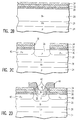
- FIG. 1A shows a region 10 of semiconductor material, for example silicon, silicon-germanium, or germanium.
- Region 10 can be doped to either N or P type conductivity, and has a concentration in the range of - to +.
- N and P refer to conductivity types, while “-" and “+” are used as appropriate to designate relative doping concentrations.
- a layer 12 of an insulating material for example silicon dioxide (SiO2) or silicon nitride (Si3N4), is disposed on the upper surface of semiconductor region 10.
- Insulating layer 12 can be formed, for example by a conventional process of thermal oxidation (to form an oxide) or chemical vapor deposition (CVD - to form an oxide or a nitride).
- an aperture 14 is formed in layer 12, exposing a portion of the surface of region 10.
- Aperture 14 can be formed by reactive ion etching (RIE), using conventional photolithographic masking, and an etchant/plasma appropriate to etch the insulating material used to form layer 12.
- RIE reactive ion etching
- a first layer 16 of a transition metal-boride compound is formed conformally over the surface of the device, including the surface of region 10 exposed within aperture 14.
- transition metal refers to those metals in groups 1B-7B, and 8 of the Periodic Table. However, the invention is preferably practiced with those metals in the 3B-6B groups of the Periodic Table. The metals in these latter groups are desirable for their ability to form selected, low resistivity compounds of the types described below.
- Layer 16 comprising TiB 2.x (where 0 ⁇ x ⁇ 10), is formed to a thickness of about 20-40 nanometers (nm).
- Layer 16 can be formed, for example, by sputtering, co-sputtering, or co-evaporation. Co-sputtering, for example, would comprise the use of titanium and boron targets.
- a layer 18 of a transition metal-nitride is formed conformally over the upper surface of layer 16.
- layer 18 will also be described with respect to the use of the transition metal titanium.
- Layer 18 formed to a thickness of about 50 nm, can be formed by processes similar to those used to form layer 16: i.e. sputtering, co-sputtering, or co-evaporation.
- the device is subjected to a thermal cycle, for example a 950_C - 1,000_C anneal for 60 seconds.
- This thermal cycle functions to drive boron ions from TiB 2.x layer 16 into semiconductor region 10, forming P doped region 20.
- Layers 16 and 18 can then be patterned (not shown), using conventional masking and etching processes, to leave registered portions overlying doped region 20 as a low resistance, ohmic contact to the doped region.
- the resulting TiN/TiB 2.x contact structure has a sheet resistance substantially lower than that of highly doped polysilicon.
- the present invention thus provides a much thinner contact structure for a given sheet resistance. This results in a more planar topography for a subsequently completed semiconductor device.
- Another advantage of the present invention is the selective etchability of the contact structure relative to silicon.
- the TiN/TiB 2.x structure is etchable in a wet etch using NH4OH + H2O2 + H2O solution (for example in a 1:1:5 ratio) at approximately 100 Angstroms/minute, providing an etching process which is very highly selective to the contact structure over the underlying silicon.
- FIGS. 2A-2D illustrate the fabrication of a vertical NPN bipolar transistor in accordance with the present invention.
- a multi-layer semiconductor substrate region 22 comprising, for example, ⁇ 100> crystallographic orientation silicon.
- Substrate region 22 includes a P type layer 24, an overlying N+ layer 26, and an overlying N- epitaxial layer 28.
- Substrate region 22 is formed, for example, by providing layer 24 from a conventional crystal pull so as to have the above-described crystallographic orientation, and a resistivity in the range of 1-20 ohm-cm.
- the surface of layer 26 is doped heavily N+, and layer 28 is grown epitaxially over layer 24 using a conventional CVD process. During this CVD process, the N+ dopant in layer 26 diffuses downward into layer 24, and upward into the epitaxial layer to provide the structure shown in FIG. 2A.
- Substrate region 22 is electrically isolated from other, similar regions (not shown) formed on the larger substrate, for example through the use of isolation trenches or field oxide isolation in a manner well known in the art. The exact type of isolation does not constitute a part of the present invention.
- a layer 30 of TiB 2.x is formed over the surface of layer 28 to a thickness of about 25 nanometers (nm).
- a layer 32 of TiN is formed over layer 30 to a thickness of about 75 nm.
- Layers 30 and 32 are formed according to the processes described for the same type layers hereinabove.
- a layer 34 of insulating material is formed over the upper surface of layer 32 to a thickness of about 100 nm.
- Layer 34 can comprise, for example an oxide, a nitride, or a nitride-over-oxide stack.
- Layer 34 is formed by a conventional process, such as thermal oxidation (for an oxide), or CVD (for an oxide or a nitride).
- conventional photolithographic masking (not shown) is used with an appropriate etching process to form an aperture 36 extending from the upper surface of layer 34 through layers 34, 32, and 30, consecutively, to expose the upper surface of layer 28.
- Appropriate etchants include a CF4 or CHF3 plasma RIE process for layer 34, and a CF4/O2 plasma RIE process (or an NH4OH + H2O2 + H2O wet etch) for layers 32 and 30.
- boron ions are implanted into the surface of layer 28 through aperture 36, using a conventional ion implant (I/I) process, to form P type region 38.
- the device is then subjected to a thermal cycle, for example at 900_C for a period of 15 minutes in an N2 environment, to drive dopant from layer 30 into layer 28, thereby forming P+ extrinsic base region 40.
- This thermal cycle further functions to cure any defects in the surface of layer 28 which might result from the I/I process used to form region 38.
- a separate anneal, subsequent to the drive-in anneal could be used to cure any surface defects.
- insulating sidewalls 42 are formed on the exposed edges of layers 30, 32, 34 within aperture 36.
- Sidewalls 42 are formed, for example, of oxide, nitride, or a stack of such materials. Sidewalls 42 are formed by conformal deposition of the insulating material(s), followed by a RIE process to leave the sidewalls.
- a layer of polycrystalline silicon (polysilicon) is formed conformally over the device and implanted with ions to an N+ conductivity type. This polysilicon layer is then patterned so as to leave N+ polysilicon region 44 filling aperture 36.
- Polysilicon region 44 is formed using a conventional CVD process, to a thickness of about 200 nm.
- the device is subjected to another thermal cycle, for example at 880_C degrees centigrade and for a duration of 20 min.
- another thermal cycle for example at 880_C degrees centigrade and for a duration of 20 min.
- dopant is driven from polysilicon region 44 into the surface of region 38, forming N type emitter region 46.
- extrinsic base region 40 is formed by out diffusion from the TiB 2.x /TiN stack 30, 32, the stack remaining as a self-aligned ohmic contact to the extrinsic base region.
- Metal contacts can be provided in a conventional manner to TiN layer 32 and emitter polysilicon region 44.
- a conventional, highly-doped reachthrough region (not shown) and metal contact can be used to make an electrical connection to subcollector region 26.
- FIGS. 3A-3C illustrate the fabrication of a vertical PNP bipolar transistor in accordance with the present invention.
- a multi-layer semiconductor substrate region 50 comprising, for example, ⁇ 100> crystallographic orientation silicon.
- Substrate region 50 includes an N type layer 52, an overlying P+ layer 56, and an overlying P- epitaxial layer 58.
- Substrate region 50 is formed, for example, by providing layer 52 from a conventional crystal pull so as to have the above-described crystallographic orientation, and a sheet resistance in the range of 1-2 ohm-cm.
- the surface of layer 52 is doped heavily P+, and layer 56 is grown epitaxially over layer 52 using a conventional CVD process. During this CVD process, the P+ dopant in layer 56 diffuses downward into layer 52, and upward into the epitaxial layer to provide the structure shown in FIG. 3A.
- Substrate region 50 is electrically isolated from other, similar regions (not shown) formed on the larger substrate, for example through the use of isolation trenches or field oxide isolation.
- isolation trenches or field oxide isolation The exact type of isolation does not constitute a part of the present invention.
- a layer 60 of N+ polysilicon is formed over the upper surface of layer 58 to a thickness of about 250 nm.
- Polysilicon layer 60 is formed by a conventional CVD process, followed by I/I to obtain the N+ conductivity.
- a layer 62 of oxide is formed over layer 60 to a thickness of about 100 nm.
- Layer 62 can be formed by CVD or thermal oxidation.
- a layer 64 of nitride is formed over layer 62, by a conventional CVD process, to a thickness of about 100 nm.
- Aperture 66 is used to define the boundary of an aperture 66, the aperture extending from the upper surface of layer 64 consecutively downward through layers 64, 62, and 60. Aperture 66 thus exposes a portion of the upper surface of layer 58. Aperture 66 can be formed using a RIE process with a CF4 plasma.
- an insulating sidewall 72 is formed over the exposed edges of layers 60, 62, and 64 within aperture 66.
- Sidewall 72 is formed by depositing a layer of insulating material, such as an oxide, a nitride, or a stack of these materials, conformally over the device. A RIE process is used to remove the horizontal portions of this insulating layer(s), leaving sidewall 72.
- a layer 74 of TiB 2.x is formed over the device, including region 68 within aperture 66, to a thickness of about 25nm.
- a layer 76 of TiN is then formed over layer 74 to a thickness of about 75nm.
- Layers 74 and 76 are formed by the processes of sputtering, co-sputtering, or co-evaporation in the manner described hereinabove.
- the device is then subjected to a thermal cycle, for example at 975 degrees centigrade for 1 minute.
- This thermal cycle drives dopant from layer 74 into the underlying surface portion of region 68, whereby to form P+ emitter region 78.
- TiN/TiB 2.x layers 76/74 are then patterned, using conventional photolithographic and etching processes, to provide a self-aligned, ohmic contact to emitter region 78.
- emitter region 78 is formed by out diffusion from the TiB 2.x /TiN stack 74, 76, the stack remaining as a self-aligned ohmic contact to the emitter region.
- Metal contacts can be provided in a conventional manner to TiN layer 76 and extrinsic base polysilicon contact region 60.
- a conventional, highly-doped reachthrough region (not shown) and metal contact can be used to make an electrical connection to subcollector region 56.
- Methods and structures utilizing a transition metal-boride/transition metal-nitride stack have thus been provided for fabricating doped semiconductor regions and self-aligned electrical contacts thereto.
- the methods are generally compatible with conventional semiconductor processing techniques and will not result in harmful reactions with silicon.
- the resulting structures yield low topography, low resistivity electrical contacts.
- the present invention has been shown to have special applicability to the formation of NPN and PNP vertical, bipolar transistors. The invention is further applicable to the formation of such transistors for very large scale integrated circuits (VLSIC).
Landscapes
- Bipolar Transistors (AREA)
- Electrodes Of Semiconductors (AREA)
Abstract
A contact is provided in a self-aligned manner to a doped region a semiconductor substrate by first forming a layer (16) of a transition metal-boride compound over a selected region (20) on the substrate (10). A layer (18) of a transition metal-nitride compound is formed over the layer (16) of transition metal-boride compound, and the structure is heated to drive dopant from the layer of transition metal-boride compound into the substrate. Finally, the transition metal-boride/transition metal nitride layers are patterned to leave the desired contact.
Description
- The present invention relates generally to semiconductor devices and more particularly to the use of a transition metal-compound as a self-aligned diffusion source and electrical contact to a doped semiconductor region.
- Many semiconductor processing applications are known wherein it is desirable to outdiffuse a dopant, into a semiconductor substrate, from a dopant source which subsequently functions as a contact to the doped substrate region. In many current applications relating to the formation of high-performance transistors, doped polysilicon is used both as the dopant source and as an ohmic contact to the diffused region. See, for example, U.S. patent 4,319,932 to Jambotkar (assigned to the assignee of the present invention), wherein polysilicon is used both as a diffusion source and contact for the extrinsic base region of a vertical, bipolar transistor. Polysilicon, however, has the disadvantage of exhibiting a relatively high sheet resistance.
- U.S. patent 4,490,193 to Ishaq et al., assigned to the assignee of the present invention, shows a method of making a diffusion into a semiconductor substrate, using a rare earth boride dopant source, wherein the rare earth boride material remains as an ohmic electrical contact to the doped region. U.S. patent 4,481,046 to Bouldin et al., also assigned to the assignee of the present invention, is similar to Ihaq et al. in that the latter teaches the use of a rare earth hexaboride material, containing a predetermined amount of silicon, for the same purposes. These rare earth boride/hexaboride materials suffer from the disadvantage of reacting with silicon at temperatures in the 1,000 + _C range. Such a reaction can damage the underlying silicon region or devices contained therein.
- Tang, T., et al., "VLSI Local Interconnect Level Using Titanium Nitride," IEDM 85, 590-593 shows a method of forming L1 level interconnects using titanium nitride (TiN) formed incidentally to the fabrication of titanium silicide (TiSi₂). More specifically, the TiN, which is incidentally formed over oxide regions during the TiSi₂ process, is selectively masked and etched to form a first level interconnect material. The TiN does not function as a dopant source.
- Roberts, S., et. al., "Method for Forming Shallow P+ Diffusions," IBM Technical Disclosure Bulletin, Vol. 30, No. 5, October 1987, pg. 404, teaches the formation of shallow P+ diffusions in silicon using sputter-deposited titanium boride as a diffusion source. The titanium boride is subsequently removed.
- U.S. patent 4,734,386 shows the use of chemical vapor-phase deposited boron nitride as a solid dopant source for diffusion doping of semiconductor substrates.
- An object of the present invention is to provide a new and improved method and structure for both solid phase doping and providing an electrical contact to a thusly doped semiconductor region.
- Another object of the present invention is to provide such a dopant source/contact having low electrical resistance.
- Yet another object of the present invention is to provide such a dopant source/contact having etch characteristics different from silicon so that the dopant source/contact can be etched selectively to silicon.
- A further object of the present invention is to provide such a dopant source/contact which is compatible with associated transistor structures.
- Yet a further object of the present invention is to provide such a dopant source/contact which does not react with silicon at conventional semiconductor processing temperatures.
- In accordance with the present invention, there is provided a new and improved method of forming a self-aligned contact to a doped region on a semiconductor substrate, comprising the steps of: providing a substrate of semiconductor material; forming a first layer of a transition metal-boride compound over at least one selected portion of the substrate; forming a second layer of a transition metal-nitride compound over the first layer; and heating to drive dopant from the first layer into the substrate.
- In accordance with another aspect of the present invention, there is provided an electrical contact to a doped region of a semiconductor substrate, comprising: a first layer of a transition metal-boride compound over at least one selected portion of the substrate; a second layer of a transition metal-nitride compound over the first layer; and a region of P type dopant in the substrate underneath the first layer.
- These and other objects, features, and advantages of the present invention will become apparent through a consideration of the following detailed description of the invention when read in conjunction with the drawing Figures, in which:
- FIGS. 1A-1C are cross-sectional views showing a method of forming a doped semiconductor region and self-aligned electrical contact in accordance with the present invention;
- FIGS. 2A-2D are cross-sectional views showing a method of forming a vertical NPN bipolar transistor in accordance with the present invention; and
- FIGS. 3A-3C are cross-sectional views showing a method of forming a vertical PNP bipolar transistor in accordance with the present invention.
- Referring now to the drawing Figures, FIG. 1A shows a
region 10 of semiconductor material, for example silicon, silicon-germanium, or germanium.Region 10 can be doped to either N or P type conductivity, and has a concentration in the range of - to +. As used herein, "N" and "P" refer to conductivity types, while "-" and "+" are used as appropriate to designate relative doping concentrations. - A
layer 12 of an insulating material, for example silicon dioxide (SiO₂) or silicon nitride (Si₃N₄), is disposed on the upper surface ofsemiconductor region 10.Insulating layer 12 can be formed, for example by a conventional process of thermal oxidation (to form an oxide) or chemical vapor deposition (CVD - to form an oxide or a nitride). - Referring now to FIG. 1B, an
aperture 14 is formed inlayer 12, exposing a portion of the surface ofregion 10.Aperture 14 can be formed by reactive ion etching (RIE), using conventional photolithographic masking, and an etchant/plasma appropriate to etch the insulating material used to formlayer 12. - Referring now to FIG. 1C, a
first layer 16 of a transition metal-boride compound is formed conformally over the surface of the device, including the surface ofregion 10 exposed withinaperture 14. As used herein, the term "transition metal" refers to those metals in groups 1B-7B, and 8 of the Periodic Table. However, the invention is preferably practiced with those metals in the 3B-6B groups of the Periodic Table. The metals in these latter groups are desirable for their ability to form selected, low resistivity compounds of the types described below. -
Layer 16, comprising TiB2.x (where 0 < x < 10), is formed to a thickness of about 20-40 nanometers (nm).Layer 16 can be formed, for example, by sputtering, co-sputtering, or co-evaporation. Co-sputtering, for example, would comprise the use of titanium and boron targets. - Still with reference to FIG. 1C, a
layer 18 of a transition metal-nitride is formed conformally over the upper surface oflayer 16. For purposes of illustration, and without limitation,layer 18 will also be described with respect to the use of the transition metal titanium. -
Layer 18, formed to a thickness of about 50 nm, can be formed by processes similar to those used to form layer 16: i.e. sputtering, co-sputtering, or co-evaporation. - Subsequent to the formation of
layer 18, the device is subjected to a thermal cycle, for example a 950_C - 1,000_C anneal for 60 seconds. This thermal cycle functions to drive boron ions from TiB2.x layer 16 intosemiconductor region 10, forming P dopedregion 20.Layers region 20 as a low resistance, ohmic contact to the doped region. - When practiced using the titanium compounds described above, the resulting TiN/TiB2.x contact structure has a sheet resistance substantially lower than that of highly doped polysilicon. The present invention thus provides a much thinner contact structure for a given sheet resistance. This results in a more planar topography for a subsequently completed semiconductor device. Another advantage of the present invention is the selective etchability of the contact structure relative to silicon. The TiN/TiB2.x structure is etchable in a wet etch using NH₄OH + H₂O₂ + H₂O solution (for example in a 1:1:5 ratio) at approximately 100 Angstroms/minute, providing an etching process which is very highly selective to the contact structure over the underlying silicon.
- FIGS. 2A-2D illustrate the fabrication of a vertical NPN bipolar transistor in accordance with the present invention.
- Referring now to FIG. 2A, a multi-layer
semiconductor substrate region 22 is shown comprising, for example, <100> crystallographic orientation silicon.Substrate region 22 includes aP type layer 24, anoverlying N+ layer 26, and an overlying N-epitaxial layer 28.Substrate region 22 is formed, for example, by providinglayer 24 from a conventional crystal pull so as to have the above-described crystallographic orientation, and a resistivity in the range of 1-20 ohm-cm. The surface oflayer 26 is doped heavily N+, andlayer 28 is grown epitaxially overlayer 24 using a conventional CVD process. During this CVD process, the N+ dopant inlayer 26 diffuses downward intolayer 24, and upward into the epitaxial layer to provide the structure shown in FIG. 2A. -
Substrate region 22 is electrically isolated from other, similar regions (not shown) formed on the larger substrate, for example through the use of isolation trenches or field oxide isolation in a manner well known in the art. The exact type of isolation does not constitute a part of the present invention. - Still with reference to FIG. 2A, a
layer 30 of TiB2.x is formed over the surface oflayer 28 to a thickness of about 25 nanometers (nm). Alayer 32 of TiN is formed overlayer 30 to a thickness of about 75 nm.Layers - Referring now to FIG. 2B, a
layer 34 of insulating material is formed over the upper surface oflayer 32 to a thickness of about 100 nm.Layer 34 can comprise, for example an oxide, a nitride, or a nitride-over-oxide stack.Layer 34 is formed by a conventional process, such as thermal oxidation (for an oxide), or CVD (for an oxide or a nitride). - Referring now to FIG. 2C, conventional photolithographic masking (not shown) is used with an appropriate etching process to form an
aperture 36 extending from the upper surface oflayer 34 throughlayers layer 28. Appropriate etchants include a CF₄ or CHF₃ plasma RIE process forlayer 34, and a CF₄/O₂ plasma RIE process (or an NH₄OH + H₂O₂ + H₂O wet etch) forlayers - Still with reference to FIG. 2C, boron ions are implanted into the surface of
layer 28 throughaperture 36, using a conventional ion implant (I/I) process, to formP type region 38. The device is then subjected to a thermal cycle, for example at 900_C for a period of 15 minutes in an N₂ environment, to drive dopant fromlayer 30 intolayer 28, thereby forming P+extrinsic base region 40. This thermal cycle further functions to cure any defects in the surface oflayer 28 which might result from the I/I process used to formregion 38. Alternatively, a separate anneal, subsequent to the drive-in anneal, could be used to cure any surface defects. - Referring now to FIG. 2D, insulating
sidewalls 42 are formed on the exposed edges oflayers aperture 36.Sidewalls 42 are formed, for example, of oxide, nitride, or a stack of such materials.Sidewalls 42 are formed by conformal deposition of the insulating material(s), followed by a RIE process to leave the sidewalls. A layer of polycrystalline silicon (polysilicon) is formed conformally over the device and implanted with ions to an N+ conductivity type. This polysilicon layer is then patterned so as to leaveN+ polysilicon region 44 fillingaperture 36.Polysilicon region 44 is formed using a conventional CVD process, to a thickness of about 200 nm. - Subsequent to the formation of
polysilicon region 44, the device is subjected to another thermal cycle, for example at 880_C degrees centigrade and for a duration of 20 min. As a result of this thermal cycle, dopant is driven frompolysilicon region 44 into the surface ofregion 38, forming Ntype emitter region 46. - There is thus formed a vertical, NPN bipolar transistor, illustrated in FIG. 2D, having
emitter region 46, intrinsic andextrinsic base regions subcollector regions extrinsic base region 40 is formed by out diffusion from the TiB2.x/TiN stack TiN layer 32 andemitter polysilicon region 44. A conventional, highly-doped reachthrough region (not shown) and metal contact can be used to make an electrical connection tosubcollector region 26. - FIGS. 3A-3C illustrate the fabrication of a vertical PNP bipolar transistor in accordance with the present invention.
- Referring now to FIG. 3A, a multi-layer
semiconductor substrate region 50 is shown comprising, for example, <100> crystallographic orientation silicon.Substrate region 50 includes anN type layer 52, an overlyingP+ layer 56, and an overlying P-epitaxial layer 58.Substrate region 50 is formed, for example, by providinglayer 52 from a conventional crystal pull so as to have the above-described crystallographic orientation, and a sheet resistance in the range of 1-2 ohm-cm. The surface oflayer 52 is doped heavily P+, andlayer 56 is grown epitaxially overlayer 52 using a conventional CVD process. During this CVD process, the P+ dopant inlayer 56 diffuses downward intolayer 52, and upward into the epitaxial layer to provide the structure shown in FIG. 3A. -
Substrate region 50 is electrically isolated from other, similar regions (not shown) formed on the larger substrate, for example through the use of isolation trenches or field oxide isolation. The exact type of isolation does not constitute a part of the present invention. - Still with reference to FIG. 3A, a
layer 60 of N+ polysilicon is formed over the upper surface oflayer 58 to a thickness of about 250 nm.Polysilicon layer 60 is formed by a conventional CVD process, followed by I/I to obtain the N+ conductivity. Alayer 62 of oxide is formed overlayer 60 to a thickness of about 100 nm.Layer 62 can be formed by CVD or thermal oxidation. Alayer 64 of nitride is formed overlayer 62, by a conventional CVD process, to a thickness of about 100 nm. - Referring now to FIG. 3B, conventional photolithographic masking (not shown) is used to define the boundary of an
aperture 66, the aperture extending from the upper surface oflayer 64 consecutively downward throughlayers Aperture 66 thus exposes a portion of the upper surface oflayer 58.Aperture 66 can be formed using a RIE process with a CF₄ plasma. - Subsequent to the formation of
aperture 66, arsenic or phosphorous ions are implanted, using a conventional I/I process, into the exposed surface oflayer 58 to form Nintrinsic base region 68. The device is then subjected to a thermal cycle, for example at 900 degrees centigrade for a period of 30 min. This thermal cycle functions to drive dopant fromlayer 60 into the underlying portions oflayer 58, forming N+extrinsic base region 70. This same thermal anneal operates to cure any defects in the surface oflayer 58 which might result from the ion implantation used to formintrinsic base region 68. Alternatively, a separate, subsequent anneal could be used to cure any such defects. - Referring now to FIG. 3C, an insulating
sidewall 72 is formed over the exposed edges oflayers aperture 66.Sidewall 72 is formed by depositing a layer of insulating material, such as an oxide, a nitride, or a stack of these materials, conformally over the device. A RIE process is used to remove the horizontal portions of this insulating layer(s), leavingsidewall 72. - In accordance with the present invention, a
layer 74 of TiB2.x is formed over the device, includingregion 68 withinaperture 66, to a thickness of about 25nm. Alayer 76 of TiN is then formed overlayer 74 to a thickness of about 75nm.Layers - The device is then subjected to a thermal cycle, for example at 975 degrees centigrade for 1 minute. This thermal cycle drives dopant from
layer 74 into the underlying surface portion ofregion 68, whereby to formP+ emitter region 78. TiN/TiB2.x layers 76/74 are then patterned, using conventional photolithographic and etching processes, to provide a self-aligned, ohmic contact toemitter region 78. - There is thus formed a vertical, PNP bipolar transistor, illustrated in FIG. 3C, having
emitter region 78, intrinsic andextrinsic base regions subcollector regions emitter region 78 is formed by out diffusion from the TiB2.x/TiN stack TiN layer 76 and extrinsic basepolysilicon contact region 60. A conventional, highly-doped reachthrough region (not shown) and metal contact can be used to make an electrical connection tosubcollector region 56. An advantage of the present invention is that of the TiN functioning as a barrier to aluminium penetration, making the present invention particularly suitable for use with aluminum metallurgy. - Methods and structures utilizing a transition metal-boride/transition metal-nitride stack have thus been provided for fabricating doped semiconductor regions and self-aligned electrical contacts thereto. The methods are generally compatible with conventional semiconductor processing techniques and will not result in harmful reactions with silicon. The resulting structures yield low topography, low resistivity electrical contacts. The present invention has been shown to have special applicability to the formation of NPN and PNP vertical, bipolar transistors. The invention is further applicable to the formation of such transistors for very large scale integrated circuits (VLSIC).
Claims (11)
- A method of forming a self-aligned contact to a doped region on a semiconductor substrate, comprising the steps of:
providing a substrate of semiconductor material;
forming a first layer of a transition metal-boride compound over at least one selected portion of said substrate;
forming a second layer of a transition metal-nitride compound over said first layer; and
heating to drive dopant from said first layer into said substrate. - A method in accordance with claim 1 and further including the step of removing portions of said first and second layers to leave overlying portions of said first and second layers as a contact to the doped region.
- A method in accordance with claim 1 wherein said transition metals are selected from the metals in groups 3B, 4B, 5B, or 6B of the Periodic Table.
- A method in accordance with claim 1 wherein said transition metals comprise titanium and said transition metal-boride comprises TiB2.x,with 0 < x < 10.
- A method in accordance with claim 1 wherein said first and second layers comprise an electrical contact to a base region of an NPN type transistor, the dopant diffused into said substrate from said first layer comprising at least a portion of the base region of said NPN transistor.
- A method in accordance with claim 1 wherein said first and second layers comprise an electrical contact to an emitter region of a PNP type transistor, the dopant diffused into said substrate from said first layer comprising at least a portion of the emitter region of said PNP transistor.
- An electrical contact to a doped region of a semiconductor substrate, comprising:
a first layer of a transition metal-boride compound over at least one selected portion of said substrate;
a second layer of a transition metal-nitride compound over said first layer; and
a region of P type dopant in said substrate underneath of said first layer. - An electrical contact in accordance with claim 7 wherein said transition metals are selected from the metals in groups 3B, 4B, 5B, or 6B of the Periodic Table.
- An electrical contact in accordance with claim 8 wherein said transition metals comprise titanium, and said transition metal boride comprises TiB2.x, with 0 < x < 10.
- An electrical contact in accordance with claim 7 wherein said first and second layers comprise an electrical contact to a base region of an NPN type transistor.
- An electrical contact in accordance with claim 7 wherein said first and second layers comprise an electrical, contact to an emitter region of a PNP type transistor.
Applications Claiming Priority (2)
| Application Number | Priority Date | Filing Date | Title |
|---|---|---|---|
| US606632 | 1990-10-31 | ||
| US07/606,632 US5086016A (en) | 1990-10-31 | 1990-10-31 | Method of making semiconductor device contact including transition metal-compound dopant source |
Publications (1)
| Publication Number | Publication Date |
|---|---|
| EP0484263A1 true EP0484263A1 (en) | 1992-05-06 |
Family
ID=24428791
Family Applications (1)
| Application Number | Title | Priority Date | Filing Date |
|---|---|---|---|
| EP91480160A Withdrawn EP0484263A1 (en) | 1990-10-31 | 1991-10-10 | Transition metal-compound dopant source and semiconductor device contact |
Country Status (3)
| Country | Link |
|---|---|
| US (1) | US5086016A (en) |
| EP (1) | EP0484263A1 (en) |
| JP (1) | JPH0744160B2 (en) |
Families Citing this family (16)
| Publication number | Priority date | Publication date | Assignee | Title |
|---|---|---|---|---|
| KR920015542A (en) * | 1991-01-14 | 1992-08-27 | 김광호 | Multi-layered wiring formation method of semiconductor device |
| US5294295A (en) * | 1991-10-31 | 1994-03-15 | Vlsi Technology, Inc. | Method for moisture sealing integrated circuits using silicon nitride spacer protection of oxide passivation edges |
| US5753530A (en) * | 1992-04-21 | 1998-05-19 | Seiko Instruments, Inc. | Impurity doping method with diffusion source of boron-silicide film |
| US5232873A (en) * | 1992-10-13 | 1993-08-03 | At&T Bell Laboratories | Method of fabricating contacts for semiconductor devices |
| US5541121A (en) * | 1995-01-30 | 1996-07-30 | Texas Instruments Incorporated | Reduced resistance base contact method for single polysilicon bipolar transistors using extrinsic base diffusion from a diffusion source dielectric layer |
| US5891791A (en) * | 1997-05-27 | 1999-04-06 | Micron Technology, Inc. | Contamination free source for shallow low energy junction implants |
| US6156630A (en) | 1997-08-22 | 2000-12-05 | Micron Technology, Inc. | Titanium boride gate electrode and interconnect and methods regarding same |
| US6214694B1 (en) | 1998-11-17 | 2001-04-10 | International Business Machines Corporation | Process of making densely patterned silicon-on-insulator (SOI) region on a wafer |
| US6211562B1 (en) * | 1999-02-24 | 2001-04-03 | Micron Technology, Inc. | Homojunction semiconductor devices with low barrier tunnel oxide contacts |
| TW471123B (en) * | 2000-07-06 | 2002-01-01 | United Microelectronics Corp | Manufacturing method for bit lines of mask ROM |
| US6399455B1 (en) * | 2001-06-15 | 2002-06-04 | National Semiconductor Corporation | Method of fabricating a bipolar transistor with ultra small polysilicon emitter |
| KR100524800B1 (en) * | 2002-09-25 | 2005-11-02 | 주식회사 하이닉스반도체 | Method for making contact plug having double doping distribution in semiconductor device |
| JP4521327B2 (en) * | 2005-07-19 | 2010-08-11 | 株式会社東芝 | Manufacturing method of semiconductor device |
| US7432164B2 (en) * | 2006-01-27 | 2008-10-07 | Freescale Semiconductor, Inc. | Semiconductor device comprising a transistor having a counter-doped channel region and method for forming the same |
| CN102129977B (en) * | 2010-01-20 | 2012-07-11 | 上海华虹Nec电子有限公司 | High-resistance resistor and method for realizing same |
| US9082722B2 (en) * | 2013-03-25 | 2015-07-14 | Raytheon Company | Monolithic integrated circuit (MMIC) structure and method for forming such structure |
Citations (4)
| Publication number | Priority date | Publication date | Assignee | Title |
|---|---|---|---|---|
| DE2454499A1 (en) * | 1974-11-16 | 1976-05-20 | Licentia Gmbh | Diffusion doping of semiconductor using reducing agent coating - over diffusion-retarding coating and windows, allowing longer doping |
| EP0096155A2 (en) * | 1982-06-07 | 1983-12-21 | International Business Machines Corporation | Transistor having emitter self-aligned with an extrinsic base contact and method of making it |
| EP0194950A2 (en) * | 1985-03-15 | 1986-09-17 | Fairchild Semiconductor Corporation | High temperature interconnect system for an integrated circuit |
| EP0305977A2 (en) * | 1987-09-04 | 1989-03-08 | Kabushiki Kaisha Toshiba | Method for doping a semiconductor integrated circuit |
Family Cites Families (15)
| Publication number | Priority date | Publication date | Assignee | Title |
|---|---|---|---|---|
| US4319932A (en) * | 1980-03-24 | 1982-03-16 | International Business Machines Corporation | Method of making high performance bipolar transistor with polysilicon base contacts |
| JPS58500680A (en) * | 1981-05-04 | 1983-04-28 | モトロ−ラ・インコ−ポレ−テツド | Semiconductor device with low resistance synthetic metal conductor and method for manufacturing the same |
| US4483726A (en) * | 1981-06-30 | 1984-11-20 | International Business Machines Corporation | Double self-aligned fabrication process for making a bipolar transistor structure having a small polysilicon-to-extrinsic base contact area |
| US4526826A (en) * | 1983-06-08 | 1985-07-02 | Kennecott Corporation | Foam semiconductor dopant carriers |
| FR2549293B1 (en) * | 1983-07-13 | 1986-10-10 | Silicium Semiconducteur Ssc | HIGH FREQUENCY BIPOLAR TRANSISTOR AND MANUFACTURING METHOD THEREOF |
| US4490193A (en) * | 1983-09-29 | 1984-12-25 | International Business Machines Corporation | Method for making diffusions into a substrate and electrical connections thereto using rare earth boride materials |
| US4481046A (en) * | 1983-09-29 | 1984-11-06 | International Business Machines Corporation | Method for making diffusions into a substrate and electrical connections thereto using silicon containing rare earth hexaboride materials |
| US4920071A (en) * | 1985-03-15 | 1990-04-24 | Fairchild Camera And Instrument Corporation | High temperature interconnect system for an integrated circuit |
| JPS62101026A (en) * | 1985-10-26 | 1987-05-11 | Shin Etsu Chem Co Ltd | Impurity diffusion source |
| US4884123A (en) * | 1987-02-19 | 1989-11-28 | Advanced Micro Devices, Inc. | Contact plug and interconnect employing a barrier lining and a backfilled conductor material |
| US4800175A (en) * | 1987-05-29 | 1989-01-24 | Owens-Illinois Television Products Inc. | Phosphorous planar dopant source for low temperature applications |
| JPH01202860A (en) * | 1988-02-09 | 1989-08-15 | Oki Electric Ind Co Ltd | Semiconductor device |
| JPH01220824A (en) * | 1988-02-29 | 1989-09-04 | Toshiba Corp | Manufacture of semiconductor device |
| JPH0666287B2 (en) * | 1988-07-25 | 1994-08-24 | 富士通株式会社 | Method for manufacturing semiconductor device |
| US4920073A (en) * | 1989-05-11 | 1990-04-24 | Texas Instruments, Incorporated | Selective silicidation process using a titanium nitride protective layer |
-
1990
- 1990-10-31 US US07/606,632 patent/US5086016A/en not_active Expired - Fee Related
-
1991
- 1991-10-10 EP EP91480160A patent/EP0484263A1/en not_active Withdrawn
- 1991-10-24 JP JP3303862A patent/JPH0744160B2/en not_active Expired - Lifetime
Patent Citations (4)
| Publication number | Priority date | Publication date | Assignee | Title |
|---|---|---|---|---|
| DE2454499A1 (en) * | 1974-11-16 | 1976-05-20 | Licentia Gmbh | Diffusion doping of semiconductor using reducing agent coating - over diffusion-retarding coating and windows, allowing longer doping |
| EP0096155A2 (en) * | 1982-06-07 | 1983-12-21 | International Business Machines Corporation | Transistor having emitter self-aligned with an extrinsic base contact and method of making it |
| EP0194950A2 (en) * | 1985-03-15 | 1986-09-17 | Fairchild Semiconductor Corporation | High temperature interconnect system for an integrated circuit |
| EP0305977A2 (en) * | 1987-09-04 | 1989-03-08 | Kabushiki Kaisha Toshiba | Method for doping a semiconductor integrated circuit |
Non-Patent Citations (5)
| Title |
|---|
| IBM TECHNICAL DISCLOSURE BULLETIN. vol. 30, no. 5, October 1987, NEW YORK US page 404 "Method for forming shallow P+ diffusions" * |
| PATENT ABSTRACTS OF JAPAN vol. 12, no. 389 (E-669) 17 October 1988, & JP-A-63 131572 (TOSHIBA CORP.) 03 June 1988, * |
| PATENT ABSTRACTS OF JAPAN vol. 12, no. 440 (E-684) 18 November 1988, & JP-A-63 172463 (MISUBISHI ELECTRIC CORP.) 16 July 1988, * |
| PROCEEDINGS OF THE 1989 BIPOLAR CIRCUITS AND TECHNOLOGY MEETING 18 September 1989, MINNEAPOLIS pages 186 - 189; J. WARNOCK et al.: "Boron doped Emitters for high performance vertical PNP transistors" * |
| THIN SOLID FILMS. vol. 153, no. 1, 26 October 1987, LAUSANNE CH pages 329 - 339; James G. RYAN et al.: "The preparation and characterization of Titanium Boride films" * |
Also Published As
| Publication number | Publication date |
|---|---|
| US5086016A (en) | 1992-02-04 |
| JPH05335266A (en) | 1993-12-17 |
| JPH0744160B2 (en) | 1995-05-15 |
Similar Documents
| Publication | Publication Date | Title |
|---|---|---|
| EP0096155B1 (en) | Transistor having emitter self-aligned with an extrinsic base contact and method of making it | |
| US5340753A (en) | Method for fabricating self-aligned epitaxial base transistor | |
| US4318751A (en) | Self-aligned process for providing an improved high performance bipolar transistor | |
| US5024957A (en) | Method of fabricating a bipolar transistor with ultra-thin epitaxial base | |
| US4381953A (en) | Polysilicon-base self-aligned bipolar transistor process | |
| EP0188291B1 (en) | Bipolar semiconductor device and method of manufacturing the same | |
| US4508579A (en) | Lateral device structures using self-aligned fabrication techniques | |
| EP0068154B1 (en) | Integrated circuit containing a semiconductive substrate having field isolation regions and electrically conductive regions | |
| US5086016A (en) | Method of making semiconductor device contact including transition metal-compound dopant source | |
| US5101256A (en) | Bipolar transistor with ultra-thin epitaxial base and method of fabricating same | |
| US4871684A (en) | Self-aligned polysilicon emitter and contact structure for high performance bipolar transistors | |
| EP0445059A2 (en) | Method for performing a complementary bipolar transistor structure including a self-aligned vertical PNP transistor | |
| EP0033495A2 (en) | Process for fabricating a high speed bipolar transistor | |
| EP0290763B1 (en) | High performance sidewall emitter transistor | |
| EP0051534B1 (en) | A method of fabricating a self-aligned integrated circuit structure using differential oxide growth | |
| JPH0630359B2 (en) | Bipolar transistor manufacturing method | |
| US6603188B1 (en) | Polysilicon-edge, low-power, high-frequency bipolar transistor and method of forming the transistor | |
| EP0042380B1 (en) | Method for achieving ideal impurity base profile in a transistor | |
| WO1999052138A1 (en) | A bipolar transistor having low extrinsic base resistance | |
| EP0388612B1 (en) | Semiconductor device with self-aligned contact to buried subcollector | |
| JPH07288284A (en) | Method for manufacturing semiconductor device | |
| JP2918248B2 (en) | Method for manufacturing semiconductor integrated circuit device | |
| EP0383712A2 (en) | Method for fabricating high performance transistors with polycrystalline silicon contacts | |
| JP2003188177A (en) | Semiconductor device having heterojunction bipolar transistor and method of manufacturing the same | |
| JPH034539A (en) | Semiconductor device and its manufacturing method |
Legal Events
| Date | Code | Title | Description |
|---|---|---|---|
| PUAI | Public reference made under article 153(3) epc to a published international application that has entered the european phase |
Free format text: ORIGINAL CODE: 0009012 |
|
| AK | Designated contracting states |
Kind code of ref document: A1 Designated state(s): DE FR GB |
|
| 17P | Request for examination filed |
Effective date: 19920817 |
|
| 17Q | First examination report despatched |
Effective date: 19940221 |
|
| STAA | Information on the status of an ep patent application or granted ep patent |
Free format text: STATUS: THE APPLICATION IS DEEMED TO BE WITHDRAWN |
|
| 18D | Application deemed to be withdrawn |
Effective date: 19940905 |