EP0484008A2 - Unité de traitement d'information avec tampon de traduction - Google Patents
Unité de traitement d'information avec tampon de traduction Download PDFInfo
- Publication number
- EP0484008A2 EP0484008A2 EP91309556A EP91309556A EP0484008A2 EP 0484008 A2 EP0484008 A2 EP 0484008A2 EP 91309556 A EP91309556 A EP 91309556A EP 91309556 A EP91309556 A EP 91309556A EP 0484008 A2 EP0484008 A2 EP 0484008A2
- Authority
- EP
- European Patent Office
- Prior art keywords
- address
- access list
- tlb
- alb
- values
- Prior art date
- Legal status (The legal status is an assumption and is not a legal conclusion. Google has not performed a legal analysis and makes no representation as to the accuracy of the status listed.)
- Withdrawn
Links
Images


Classifications
-
- G—PHYSICS
- G06—COMPUTING; CALCULATING OR COUNTING
- G06F—ELECTRIC DIGITAL DATA PROCESSING
- G06F12/00—Accessing, addressing or allocating within memory systems or architectures
- G06F12/02—Addressing or allocation; Relocation
- G06F12/08—Addressing or allocation; Relocation in hierarchically structured memory systems, e.g. virtual memory systems
- G06F12/10—Address translation
- G06F12/1027—Address translation using associative or pseudo-associative address translation means, e.g. translation look-aside buffer [TLB]
- G06F12/1036—Address translation using associative or pseudo-associative address translation means, e.g. translation look-aside buffer [TLB] for multiple virtual address spaces, e.g. segmentation
Definitions
- the present invention relates to an improvement of an information processing unit having a translation buffer including a TLB, an ALB or the like.
- the buffer is generally called a TLB (Translation Lookaside Buffer).
- the TLB is usually constituted by a RAM (Random Access Memory).
- a direct mapping method is used and when there is more than one way, a set-associative method is used.
- the address of RAM uses a portion of a virtual address or an operated value of the whole or a portion of a virtual address.
- the read of RAM by the operated value is generally called hashing.
- an access register translation is explained.
- an information processing unit using a plurality of virtual address space to designate a segment table for translation from a virtual address to a real address
- an access register translation is executed.
- the detail of the access register translation is described in the manual of International Business Machines Corporation," IBM Enterprise System Architecture/370 (SA22-7200-0)" and "NIKKEI COMPUTER 1988, September 12".
- ALB Access Register Translation Lookaside Buffer
- This invention relates to an improvement of the information processing unit having a TLB, an ALB, or the like.
- the details of the related arts concerning the TLB and ALB are explained hereinafter in the DESCRIPTION OF THE PREFERRED EMBODIMENTS with reference to drawings.
- the RAM in the conventional constitution of the TLB, since the index address is only the virtual address and in the conventional constitution of the ALB, since the index address is only an access list entry number, the RAM sometimes used is one-sided, and as a result, the hit ratio of the TLB or ALB is reduced.
- the storage of the translated result to the TLB sometimes cannot be carried out as a whole simultaneously by collected access to one special line.
- the translated result excluded from the TLB must be translated again when the translation becomes necessary and the other translated result, currently stored in the TLB, is excluded and the necessary translated data is stored.
- the frequent occurrence of this operation is called thrashing and the occurrence of thrashing causes low performance.
- the present invention is carried out with this problem in mind.
- An object of the present invention is to prevent thrashing and increase the hit ratio in a TLB or an ALB.
- an information processing unit including a TLB using a direct mapping method or a set-associative method having a plurality of TLB entries having a pair of at least a virtual address and a real address or an absolute address, which is a translated result of the virtual address, to translate the address from the virtual address to the real address or the absolute address, characterized in that the unit comprises a translation buffer for operating predetermined operations among three values of a virtual address, a segment table origin address used in the translation of the virtual address and a virtual machine identifier, or between selected two values from the above three values, for reading the TLB by an index address obtained by the operating result.
- an information processing unit including an ALB using a direct mapping method or a set-associative method, having a plurality of ALB entries having a pair of at least an access list entry number and a segment table designation, which is a translated result of the access list entry number, to translate an access register from the access list entry number to the segment table designation, characterized in that the unit comprises a translation buffer for operating predetermined operations among three values of an access list entry number, an access list designation source origin used in the translation of the access list entry number, and a virtual machine identifier, or between selected two values from the above three values, for reading the ALB by an index address obtained by the operating result.
- Figure 1 is a diagram showing a translation process to translate a virtual address to a real address.
- STO denotes a segment table origin address
- PTO denotes a page table origin address
- PFRA denotes a page frame real address
- SX denotes a segment index
- PX denotes a page index
- BX denotes a byte index.
- the segment table origin address STO is designated.
- the segment table origin address STO is added to the segment index SX of the virtual address, then, from the additional result, the corresponding entry of the segment table is accessed.
- the page table origin address PTO is stored.
- the read page table origin address PTO is added to the page index PX of the virtual address, and from the additional result, the corresponding entry of the page table is read.
- the page frame real address PFRA is stored. By the concatenation of the read page frame real address PFRA and the byte index BX of the virtual address, the real address corresponding to the virtual address is obtained.
- the segment table and the page table are included in the main storage.
- Fig. 2 the constitution of the conventional TLB is shown.
- 1 denotes an operation circuit
- 2 denotes a RAM of the TLB
- 3 to 5 denote comparison circuits
- 6 denotes a AND circuit
- 7 denotes a selector
- V denotes a bit showing a validity
- VMID denotes a virtual machine identifier
- STO denotes a segment table origin
- VIR denotes a virtual address
- REAL denotes a real address
- etc. denotes the other fields.
- the operation of the TLB in Fig. 2 is explained below.
- the virtual address (bits 01 to 19) is applied to the operation circuit 1.
- the operation circuit 1 executes operations shown in Fig. 3 and outputs an index address of eight bits. In this place, a mark denotes an EOR (exclusive-OR) circuit.
- the RAM 2 is accessed in accordance with the index address and the corresponding TLB entry is read from the RAM 2.
- the TLB entry consists of the validity bit V, the virtual machine identifier VMID, the segment table origin STO, the virtual address VIR, the real address REAL, and other fields.
- the virtual machine identifier VMID of the read TLB entry is compared with the virtual machine identifier from an external by the comparison circuit 3, the segment table origin STO of the read TLB entry is compared with the segment table origin from an external by the comparison circuit 4, and the virtual address VIR of the read TLB entry is compared with the virtual address from an external by the comparison circuit 5.
- the validity bit of the read TLB entry and the compared results from the comparison circuits 3 to 5 are supplied to the AND circuit 6.
- each of the portions shown by the reference numerals 2, 3, 4, 5, and 6 exists in double, respectively.
- the outputs of the two AND circuits 6 are supplied to the selector 7.
- the selector 7 selects a real address REAL, which is read from the RAM 2 corresponding to the AND circuit 6 showing logical "1", and outputs the same.
- FIG. 4 shows an access register translation.
- ALDSO denotes an access list designation source origin
- ALET denotes an access list entry token
- ALO denotes an access list origin
- ALEN denotes an access list entry number
- ASTEA denotes an ASN second table entry address
- STD denotes a segment table designation
- PSTD denotes a primary segment table designation
- SSTD denotes a secondary segment table designation.
- the access list designation source origin ALDSO is designated, the main storage is accessed in accordance with the access list designation source origin ALDSO, and the access list origin ALO is read. Moreover, the access list entry token ALET designated in the access register is read. In the access list entry token ALET, the access list entry number ALEN is included. The read access list origin ALO is added to the read access list entry number ALEN, and the corresponding entry of the access list is accessed in accordance with the additional result. In the access list entry, the ASN second table entry address ASTEA is included. The corresponding entry of the ASN second table is read in accordance with the read ASN second table entry address ASTEA. In the ASN second table entry, the segment table designation STD is included.
- control register CR1 In a control register CR1, the primary segment table designation PSTD is stored and in a control register CR7, the secondary segment table designation SSTD is stored.
- the primary segment table designation PSTD of the control register CR1 is selected, when the low order end bit of the access list entry token ALET is "1" and the other bits are "0", the secondary segment table designation SSTD of the control register CR7 is selected, and in cases except for the above, the segment table designation STD of the ASN second table entry is selected.
- Figure 5 shows a constitution of the conventional ALB.
- 11 denotes an operation circuit
- 12 denotes a RAM of the ALB
- 13 to 15 denote comparison circuits
- 16 denotes an AND circuit
- 17 denotes a selector.
- An access list entry number (bits 00 to 15) is supplied to the operation circuit 11.
- the operation circuit 11 operates as shown in Fig. 6, and an index address of 8 bits is output.
- the RAM 12 is accessed in accordance with the index address, and the corresponding ALB entry is read from the RAM 12.
- the ALB entry consists of a validity bit V, a virtual machine identifier VMID, an access list designation source origin ALDSO, an access list entry number ALEN, a segment table designation STD, and other fields, etc.
- the virtual machine identifier VMID of the read ALB entry is compared with the virtual machine identifier from an external by the comparison circuit 13, the access list designation source origin ALDSO of the read ALB entry is compared with the access list designation source origin from an external by the comparison circuit 14, and the access list entry number ALEN of the read ALB entry is compared with the access list entry number from an external by the comparison circuit 15.
- the validity bit V of the read ALB entry and the compared result in the identity circuits 13 to 15 are supplied to the AND circuit 16.
- each of the portions having reference numerals 12, 13, 14, 15, and 16 exist in double, respectively.
- the outputs of the two AND circuits 16 is supplied to the selector 17.
- the selector 17 selects the segment table designation STD that is read from the RAM 12 corresponding to the AND circuit 16 designating logical "1".
- the TLB has a plurality of TLB entries each having at least a pair of virtual addresses and real addresses (or absolute addresses).
- a virtual machine identifier, a segment table origin address, and a virtual address are supplied to an operation circuit, and the operation circuit forms an index address in accordance with the above input data.
- the data of a TLB entry determined by the index address and output from the operation circuit is read from the TLB.
- the TLB having a pair of virtual addresses and absolute addresses in the TLB entry is known.
- This invention can be applied to the above known TLB.
- the absolute address is prefixed to the real address.
- the index address can be formed by using two input data of three input data, which are the virtual machine identifier, the segment table origin address and the virtual address.
- FIG. 8 An embodiment according to a first aspect of the present invention is explained with reference to Fig. 8.
- 21 denotes an operation circuit
- 22 denotes a RAM of the TLB
- 23 to 25 denote comparison circuits
- 26 denotes an AND circuit
- 27 denotes a selector.
- the virtual machine identifier (bits 0 to 3), the segment table origin (bits 01 to 19), and the virtual address (bits 01 to 19) are supplied.
- the virtual machine identifier and the segment table origin are stored in a register (VMID-REG) and a register (STO-REG) in the information processing unit, respectively.
- Figure 9 shows an example of the operation executed in the operation circuit 21.
- M0 to M3 shows each bit of the virtual machine identifier
- S01 to S19 show each bit of the segment table origin
- V01 to V19 show each bit of the virtual address.
- the operation circuit 21 forms, for example, bit 0 of the index address in accordance with the following equation.
- the virtual addresses that are included in a special scope are frequently utilized.
- the address in the value of low order is apt to be used frequently. In this case, if the operation according to this invention is executed, the whole TLB is used uniformly and the ratio of hit increases.
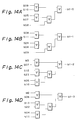
- Figs. 10A to 10H The logical circuits corresponding to the logical equations shown in Fig. 9 are shown in Figs. 10A to 10H.
- the hashing operation is executed by using the virtual address, the segment table origin address, and the virtual machine identifier, two of the three above can also be used.
- the ALB comprises a plurality of ALB entries having at least a pair of access list entry numbers and a segment table designation that is a translated result.
- a virtual machine identifier, an access list designation source origin, and an access list entry number are supplied to an operation circuit, and the operation circuit forms an index address in accordance with the input data.
- the data of the ALB entry determined by the index address, output from the operation circuit, are read from the ALB.
- the index address may be formed in accordance with the two input data of the three input data, i.e., the virtual machine identifier, the access list designation source origin, and the access list entry number.
- 31 denotes an operation circuit
- 32 denotes a RAM of the ALB
- 33 to 35 denote comparison circuits
- 36 denotes an AND circuit
- 37 denotes a selector.
- a virtual machine identifier (bits 0 to 3), an access list designation source origin (bits 01 to 25), and an access list entry number (bits 00 to 15) are supplied to the operation circuit 31.
- the virtual machine identifier and the access list designation source origin are stored in a register (VMID-REG) and a register (ALDSO-REG) in the information processing unit, respectively.
- VMID-REG a register
- ALDSO-REG a register
- M0 to M3 shows each bit of the virtual machine identifier
- S01 to S25 show each bit of the access list designation source origin
- N00 to N15 show each bit of the access list entry number.
- the operation circuit 31 generates, for example, bit 0 of the index address in accordance with an equation: S09 S10 S25 N07 N08. In this place the mark designates an EOR (exclusive-OR) circuit.
- the RAM 32 of the ALB is accessed by the index address generated by the operation circuit 31.
- the operation hereinafter is the same as that of the conventional ALB in Fig. 5.
- the logical circuits executing the operation in Fig. 13 are shown in Figs. 14A to 14H.
- the read of RAM by the above operated value is called hashing operation.
- any access list designation source origin or under any virtual machine, a special scope of access list entry number is frequently used.
- the low order of the entry number is apt to be used frequently.
- the operation according to this invention is applied, the whole ALB is used uniformly and the hit ratio of the ALB increases.
- the hashing operation is executed by using the access list entry number, the access list designation source origin, and the virtual machine identifier, two of the three above can also be used.
- Figure 15 is a block diagram showing a situation of the TLB and the ALB in a central processing unit (CPU) in the information processing unit.
- CPU central processing unit
- the CPU comprises an I-unit, an E-unit, and an S-unit.
- the I-unit controls the execution of the instruction.
- the E-unit entirely executes the calculation.
- the S-unit receives the request of the instruction read, the operand read or the operand write from the I-unit, and then after the access register translation and the address translation, the S-unit accesses a cache.
- the S-unit sends the read data to the I-unit; for the request of the operand read, the S-unit sends the read data to the E-unit; and for the request of the operand write, the S-unit writes the Store-Data from the E-unit into the cache. If necessary, the cache transmits the data to the main memory or receives the data from the main memory.
- GRs general registers
- ARs access registers
- CRs control registers
- I-unit and E-unit One data is selected from the ARs, the selected output is sent to the S-unit as an access list entry number (ALEN).
- ALEO access list entry number
- VMID virtual machine identifier
- ALDSO access list designation source origin
Landscapes
- Engineering & Computer Science (AREA)
- Theoretical Computer Science (AREA)
- Physics & Mathematics (AREA)
- General Engineering & Computer Science (AREA)
- General Physics & Mathematics (AREA)
- Memory System Of A Hierarchy Structure (AREA)
Applications Claiming Priority (2)
| Application Number | Priority Date | Filing Date | Title |
|---|---|---|---|
| JP282444/90 | 1990-10-20 | ||
| JP2282444A JPH0690688B2 (ja) | 1990-10-20 | 1990-10-20 | 変換バッファを具備する情報処理装置 |
Publications (2)
| Publication Number | Publication Date |
|---|---|
| EP0484008A2 true EP0484008A2 (fr) | 1992-05-06 |
| EP0484008A3 EP0484008A3 (en) | 1993-05-19 |
Family
ID=17652502
Family Applications (1)
| Application Number | Title | Priority Date | Filing Date |
|---|---|---|---|
| EP19910309556 Withdrawn EP0484008A3 (en) | 1990-10-20 | 1991-10-17 | Information processing unit having translation buffer |
Country Status (2)
| Country | Link |
|---|---|
| EP (1) | EP0484008A3 (fr) |
| JP (1) | JPH0690688B2 (fr) |
Cited By (1)
| Publication number | Priority date | Publication date | Assignee | Title |
|---|---|---|---|---|
| WO2009001153A1 (fr) * | 2007-06-28 | 2008-12-31 | Nokia Corporation | Unité de protection de mémoire dans un environnement de traitement virtuel |
Families Citing this family (1)
| Publication number | Priority date | Publication date | Assignee | Title |
|---|---|---|---|---|
| KR101770495B1 (ko) * | 2014-07-21 | 2017-08-22 | 비아 얼라이언스 세미컨덕터 씨오., 엘티디. | 공통 상황 항목의 동시 무효화를 지원하는 어드레스 변환 캐시 |
Citations (4)
| Publication number | Priority date | Publication date | Assignee | Title |
|---|---|---|---|---|
| JPS5733477A (en) * | 1980-07-31 | 1982-02-23 | Fujitsu Ltd | Computer system |
| EP0327839A2 (fr) * | 1988-02-10 | 1989-08-16 | International Business Machines Corporation | Système de traitement d'informations |
| DE4019961A1 (de) * | 1989-06-23 | 1991-01-10 | Hitachi Ltd | Steuerung fuer mehrfache virtuelle adressraeume |
| JPH1010359A (ja) * | 1996-06-21 | 1998-01-16 | Ando Electric Co Ltd | 光結合器 |
Family Cites Families (1)
| Publication number | Priority date | Publication date | Assignee | Title |
|---|---|---|---|---|
| JPS63177239A (ja) * | 1987-01-19 | 1988-07-21 | Hitachi Ltd | 仮想計算機システム |
-
1990
- 1990-10-20 JP JP2282444A patent/JPH0690688B2/ja not_active Expired - Fee Related
-
1991
- 1991-10-17 EP EP19910309556 patent/EP0484008A3/en not_active Withdrawn
Patent Citations (4)
| Publication number | Priority date | Publication date | Assignee | Title |
|---|---|---|---|---|
| JPS5733477A (en) * | 1980-07-31 | 1982-02-23 | Fujitsu Ltd | Computer system |
| EP0327839A2 (fr) * | 1988-02-10 | 1989-08-16 | International Business Machines Corporation | Système de traitement d'informations |
| DE4019961A1 (de) * | 1989-06-23 | 1991-01-10 | Hitachi Ltd | Steuerung fuer mehrfache virtuelle adressraeume |
| JPH1010359A (ja) * | 1996-06-21 | 1998-01-16 | Ando Electric Co Ltd | 光結合器 |
Non-Patent Citations (2)
| Title |
|---|
| PATENT ABSTRACTS OF JAPAN vol. 006, no. 100 (P-121)9 June 1982 & JP-A-57 033 477 ( FUJITSU ) 23 February 1982 * |
| PATENT ABSTRACTS OF JAPAN vol. 013, no. 180 (P-864)27 April 1989 & JP-A-10 10 359 ( HITACHI ) 13 January 1989 * |
Cited By (2)
| Publication number | Priority date | Publication date | Assignee | Title |
|---|---|---|---|---|
| WO2009001153A1 (fr) * | 2007-06-28 | 2008-12-31 | Nokia Corporation | Unité de protection de mémoire dans un environnement de traitement virtuel |
| US8661181B2 (en) | 2007-06-28 | 2014-02-25 | Memory Technologies Llc | Memory protection unit in a virtual processing environment |
Also Published As
| Publication number | Publication date |
|---|---|
| EP0484008A3 (en) | 1993-05-19 |
| JPH04156638A (ja) | 1992-05-29 |
| JPH0690688B2 (ja) | 1994-11-14 |
Similar Documents
| Publication | Publication Date | Title |
|---|---|---|
| KR100382395B1 (ko) | 컴퓨터메모리에정보를기억하는방법및장치 | |
| US5295251A (en) | Method of accessing multiple virtual address spaces and computer system | |
| US6256715B1 (en) | System and method of performing gateway access | |
| US6145064A (en) | Method of efficiently updating hashed page tables | |
| US4654777A (en) | Segmented one and two level paging address translation system | |
| US5475827A (en) | Dynamic look-aside table for multiple size pages | |
| EP1096385B1 (fr) | Procédé et dispositif pour former l'adresse d'une rubrique | |
| US6014732A (en) | Cache memory with reduced access time | |
| US4453212A (en) | Extended address generating apparatus and method | |
| EP0149389B1 (fr) | Système de commande de traduction d'adresse | |
| US5060137A (en) | Explicit instructions for control of translation lookaside buffers | |
| US4792897A (en) | Address translation unit for translation of virtual address to real address using translation tables of multi-level hierarchical structure | |
| US5630087A (en) | Apparatus and method for efficient sharing of virtual memory translations | |
| US6363336B1 (en) | Fine grain translation discrimination | |
| US5555395A (en) | System for memory table cache reloads in a reduced number of cycles using a memory controller to set status bits in the main memory table | |
| JPH04319747A (ja) | アドレス変換機構 | |
| US5305444A (en) | Apparatus for increasing the number of hits in a translation lookaside buffer including instruction address lookaside register | |
| US5226132A (en) | Multiple virtual addressing using/comparing translation pairs of addresses comprising a space address and an origin address (sto) while using space registers as storage devices for a data processing system | |
| EP0410740B1 (fr) | Système et méthode de commande d'accès à l'espace d'adressage de mémoire virtuelle | |
| US6412056B1 (en) | Extended translation lookaside buffer with fine-grain state bits | |
| EP0519685A1 (fr) | Traduction d'adresse | |
| US6598050B1 (en) | Apparatus and method for limited data sharing in a multi-tasking system | |
| CA1262287A (fr) | Instructions explicites pour controler les repertoires de pages actives | |
| US5341485A (en) | Multiple virtual address translation per computer cycle | |
| US6574698B1 (en) | Method and system for accessing a cache memory within a data processing system |
Legal Events
| Date | Code | Title | Description |
|---|---|---|---|
| PUAI | Public reference made under article 153(3) epc to a published international application that has entered the european phase |
Free format text: ORIGINAL CODE: 0009012 |
|
| AK | Designated contracting states |
Kind code of ref document: A2 Designated state(s): DE FR GB |
|
| PUAL | Search report despatched |
Free format text: ORIGINAL CODE: 0009013 |
|
| AK | Designated contracting states |
Kind code of ref document: A3 Designated state(s): DE FR GB |
|
| 17P | Request for examination filed |
Effective date: 19930726 |
|
| 17Q | First examination report despatched |
Effective date: 19970313 |
|
| STAA | Information on the status of an ep patent application or granted ep patent |
Free format text: STATUS: THE APPLICATION IS DEEMED TO BE WITHDRAWN |
|
| 18D | Application deemed to be withdrawn |
Effective date: 19970724 |