EP0482828A2 - Message-oriented bank controller interface - Google Patents
Message-oriented bank controller interface Download PDFInfo
- Publication number
- EP0482828A2 EP0482828A2 EP91309605A EP91309605A EP0482828A2 EP 0482828 A2 EP0482828 A2 EP 0482828A2 EP 91309605 A EP91309605 A EP 91309605A EP 91309605 A EP91309605 A EP 91309605A EP 0482828 A2 EP0482828 A2 EP 0482828A2
- Authority
- EP
- European Patent Office
- Prior art keywords
- register
- controller unit
- data
- bank controller
- message
- Prior art date
- Legal status (The legal status is an assumption and is not a legal conclusion. Google has not performed a legal analysis and makes no representation as to the accuracy of the status listed.)
- Granted
Links
- 230000002093 peripheral effect Effects 0.000 claims abstract description 46
- 230000005540 biological transmission Effects 0.000 claims abstract description 10
- 238000004891 communication Methods 0.000 abstract description 9
- 238000001514 detection method Methods 0.000 abstract description 3
- 238000012546 transfer Methods 0.000 description 9
- 230000006870 function Effects 0.000 description 8
- 238000010586 diagram Methods 0.000 description 4
- 238000012360 testing method Methods 0.000 description 2
- 230000002457 bidirectional effect Effects 0.000 description 1
- 238000011161 development Methods 0.000 description 1
- 230000000694 effects Effects 0.000 description 1
- 238000005516 engineering process Methods 0.000 description 1
- 238000012986 modification Methods 0.000 description 1
- 230000004048 modification Effects 0.000 description 1
- 230000008520 organization Effects 0.000 description 1
- 238000012545 processing Methods 0.000 description 1
- 239000007787 solid Substances 0.000 description 1
Images


Classifications
-
- H—ELECTRICITY
- H04—ELECTRIC COMMUNICATION TECHNIQUE
- H04L—TRANSMISSION OF DIGITAL INFORMATION, e.g. TELEGRAPHIC COMMUNICATION
- H04L51/00—User-to-user messaging in packet-switching networks, transmitted according to store-and-forward or real-time protocols, e.g. e-mail
- H04L51/21—Monitoring or handling of messages
-
- H—ELECTRICITY
- H04—ELECTRIC COMMUNICATION TECHNIQUE
- H04L—TRANSMISSION OF DIGITAL INFORMATION, e.g. TELEGRAPHIC COMMUNICATION
- H04L12/00—Data switching networks
- H04L12/28—Data switching networks characterised by path configuration, e.g. LAN [Local Area Networks] or WAN [Wide Area Networks]
- H04L12/40—Bus networks
- H04L12/407—Bus networks with decentralised control
- H04L12/417—Bus networks with decentralised control with deterministic access, e.g. token passing
-
- H—ELECTRICITY
- H04—ELECTRIC COMMUNICATION TECHNIQUE
- H04L—TRANSMISSION OF DIGITAL INFORMATION, e.g. TELEGRAPHIC COMMUNICATION
- H04L9/00—Cryptographic mechanisms or cryptographic arrangements for secret or secure communications; Network security protocols
- H04L9/40—Network security protocols
Definitions
- This invention relates to message-oriented digital communication, such as that which can be utilized between a Bank Controller Unit and peripheral devices.
- digital transmission occurs between a central office terminal and a remote terminal, and between a remote terminal and the subscribers.
- the various units of the remote terminal such as channel units, are controlled by a Bank Controller Unit which communicates with the various peripheral units through a register-oriented interface.
- a circuit for transmitting and receiving a digital stream including multiple bytes of data and control signals where the circuit comprises at least four registers.
- a first register is adapted to receive control signals which are part of the digital stream, while a second register is adapted to transmit control signals as part of the digital stream.
- a third register is adapted to receive data which is part of the digital stream, while a fourth register is adapted to transmit data as part of the digital stream.
- a fifth register may also be included to store data transmitted by the fourth register and to transmit the data in the event of an error in transmitting the data from the fourth register.
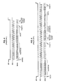
- FIG. 1 is a block diagram illustrating a typical Bank Controller Unit link to peripheral devices in the central office terminal or remote terminal of a digital loop transmission system.
- the Bank Controller Unit (BCU), 10, includes a microprocessor, 11, which communicates to a Serial Control Link Driver (SCLD), 12, which is usually part of an Alarm and Display Unit (ADU), 13. Communication takes place over a Data/Address (D/A) bus 28.
- the Serial Control Link Driver, 12 communicates with each Bank Peripheral Device (BPD), such as 14, by means of two sets of leads, designated NP and NQ leads, 15 and 16, respectively, as well as a bidirectional serial data bus 17.
- BPD Bank Peripheral Device
- One NP lead, one NQ lead and the data bus terminate on a Bank Control Link Terminator, e.g., 18, which is part of each peripheral device's circuitry.
- the NP and NQ leads jointly select the peripheral device, while the data pass over the data bus in both directions.
- the terminator includes registers (not shown) which can be accessed by the peripheral device's microprocessor 19.
- Each peripheral device, 14, also has a service request (SR) lead, 20, which is coupled directly to the Bank Controller Unit, 10, and which is shared among several peripheral devices.
- SR service request
- This lead can provide an interrupt function during the normal BCU communication with the peripheral device.
- the BCU, 10 would command the SCLD, 12, to send a message typically containing eight bits of data to a specified register of a peripheral device.
- the SCLD would then send the message to the terminator of the peripheral device, 14, as further illustrated in FIG. 4 along with the waveforms of the NP and NQ leads to that peripheral device.
- the message consisted of a read/write select bit, 16 message bits and a parity bit.
- the 16 message bits, as shown, were, typically, divided into an address field (A0 - A7) that identified the register designated to receive the message, and a data field (D0 - D7) that contained the data to be written into the register.
- the peripheral device would send back two check code bits (C0 - C1) to indicate whether received and calculated parity agreed and whether the register address was valid.
- the Serial Control Link Driver (SCLD), 12 would send a message in the same format, but with the read/write select bit set to "read" and the data field containing all zeros as further illustrated in FIG. 5.
- the peripheral device would send back two check code bits (C0 - C1), 16 message bits, and a parity bit (P).
- the message bits would be divided into an address field (A0 - A7) that identified the register being read and a data field (D0 - D7) containing the data in that register.
- the SCLD would also test for a match between received and calculated parity. After each read and write operation, the BCU would read a register on the SCLD, which register's content would indicate whether the operation was error-free. In the case of an error-thee read operation, the BCU would read yet another register in the SCLD, which register would contain the data obtained from the peripheral device. If an error were reported, the BCU would try again. For additional error protection on a read operation, the BCU would compare the address register information in the messages transmitted and received by the SCLD.
- each peripheral device is provided with at least four, and preferably five, registers which are dedicated to message-oriented communication with that device, as illustrated in the block diagram of FIG. 2.
- Each register, 21-25, in this example is 8-bits wide.
- the register, 21, labeled "SIG_OUT”, receives outgoing control signals, while the register, 22, labeled "DATA_OUT” receives outgoing message data.
- Outgoing refers to communication from the BCU toward the peripheral device, while "Incoming” denotes communication from the peripheral device to the BCU.) Incoming communication is handled by three registers.
- Register, 23, labeled “SIG_IN” receives control signals from the peripheral device, while register, 24, labeled “DATA_IN1” receives the data messages.
- the final, optional, register, 25, labeled “DATA_IN2” holds the last byte read by the SCLD from "DATA_IN1". In case there is an error, this byte can then be re-read by the SCLD from this auxiliary register.
- Control circuitry, 26 and 27, provides several functions including selecting a register, deciding whether the chosen register is to be read or written, determining whether an error has occurred in transmission from the BCU, and notifying the BCU or peripheral device's microprocessor whether a transmission error has occurred. Notifying the BCU of an error in an outgoing message can be accomplished by controlling the value of the check code, previously mentioned.
- the peripheral device Whenever the SIG_IN register, 23, contains a control signal value other than IDLE, the peripheral device will assert a service request toward the BCU on the service request lead, 20. This feature enables the BCU to recognize a pending information transfer without periodically polling the SIG_IN registers, which polling would divert a portion of the BCU's processing capacity from other tasks.
- a signal value of IDLE in the SIG_IN register causes the service request to be retired. In this example, the IDLE value is zero.
- flow control is implemented by using a new value of the check code.
- Flow control ensures that the BCU does not send or receivee data faster than the peripheral device can receive or send the data, respectively.
- the BCU should not write a byte into the BPD's DATA_OUT register until the peripheral device's microprocessor (19) has copied the previous byte from DATA_OUT, and the BCU should not read the BPD's DATA_IN1 register while it contains data previously read by the BCU or the DATA_IN2 register while it does not contain current data.
- the check code will indicate that the register is BUSY.
- the terminator will send out a newly designated value of the existing two-bit check code to indicate this fact to the BCU. That is, the newly designated value of ⁇ 1,1 ⁇ indicates a good pity, a valid register address, but a busy data register.
- FIG. 3 illustrates the message format utilized in accordance with the invention.
- the message is transferred from the BCU to the peripheral device via the DATA_OUT register, 22, or from the peripheral device to the BCU via the DATA_IN1 and DATA_IN2 registers, 24 and 25, respectively.
- Each division indicates one byte of the message.
- the first two bytes, 31 and 32, labeled “Length (Lower)” and “Length (Upper)” indicate to the receiver the total length of the message, including the length bytes themselves and the Stop and Checksum bytes (40 and 41, respectively).
- the Length (Lower) byte contains the least significant eight bits of the binary number representing the length.
- the Length (Upper) byte contains the most significant eight bits of the number representing the length.
- the Physical Target (Coarse) byte, 33 designates the particular central office or remote terminal to which the message will be sent.
- the Physical Target (Fine) byte, 34 indicates the particular circuit card in the central office or remote terminal to which the message will be sent.
- the Firmware Target (Coarse) byte, 35 designates the broad category of firmware or software which will receive the message (e.g., the firmware which handles inventory control), while the Firmware Target (Fine) byte, 36, indicates the specific function of the destination firmware object (e.g., the function of accepting inventory information from a peripheral device).
- the Physical Source (Coarse) byte, 37 designates the central office or remote terminal from which the message is transmitted, while the Physical Source (Fine) byte indicates the circuit card within the central office or remote terminal from which the message originates.
- the above-described header bytes are followed by the Information bytes, 39, which contain the payload of the message (i.e., the block of data whose transfer is the ultimate purpose of the invention). It is contemplated that the Information portion of the message may have any length from zero to 65,525 bytes, and can have any content, since the data and control signals will be handled by different registers.
- the Information is followed by a Stop byte, 40, with a fixed value. This byte serves as part of the error detection capability of the system by verifying that the number of bytes received in the message is equal to the number of bytes promised in the Length bytes (31 and 32). The remainder of the error detection capability is provided by the Checksum byte 41.
- Each bit in the Checksum byte is the exclusive OR function of the corresponding bits in all the bytes previously received in the message starting with Length byte 31 and ending with Stop byte 40.
- the exclusive OR function will be calculated for each of the other bits in the Checksum byte.
- Stop and Checksum bytes are particularly useful in digital loop systems since the peripheral devices tend to have small (8-bit) processors and limited memory space (typically less than 256 bytes of RAM and less than 4 Kbytes of ROM). Further, the use of the Stop byte in addition to the Checksum byte is desirable for reducing still further the probability of failing to detect an error in the length bytes.
- Table I below indicates in more detail a typical message transfer from the Bank Controller Unit (BCU) to the Bank Peripheral Device (BPD).
- the first column designates the function performed by the BCU, the second column designates the register employed, and the third column designates the function performed by the BPD.
- the arrows between columns illustrate the direction of transfer of the control signal bytes and data bytes.
- the solid double arrow indicates a service request asserted by the BPD, while the dotted double arrow indicates retiring of a service request.
- the BCU first writes a Request to Send (RTS) signal into the SIG_OUT register (see FIG. 2) which is read by the BPD.
- the BPD then writes a Clear to Send (CTS) signal into the SIG_IN register which is read by the BCU.
- CTS Clear to Send
- SMO Start of Message Out
- IDLE Idle signal
- the BCU then writes the data bytes (31 to 41 inclusive in FIG. 3) one byte at a time into the DATA_OUT register, where they are read out one byte at a time by the BPD.
- the BPD If, at any time, the BPD responds to an offered byte with a busy check code, the BCU saves the byte and tries again later. After the last (Checksum) byte is read, the BPD compares the Checksum byte with the checksum that the BPD has calculated as it received the message. Assuming no errors are present, the BPD acknowledges the message to the BCU by writing Message Acknowledge (MACK) in the SIG_IN register. The BCU then indicates the End of Message in the SIG_OUT register, and the BPD retires the service request by writing an Idle signal in the SIG_IN register.
- MACK Message Acknowledge
- BPD_BSY BPD Busy
- Table II illustrates a typical message transfer from the BPD to the BCU.
- the BPD begins by writing the first data byte into both the DATA_IN1 and DATA_IN2 registers.
- the BPD then writes a Request to Send signal into the SIG_IN register where it is read by the BCU.
- the BCU responds by writing a Start of Message In signal into the SIG_OUT register which is read by the BPD.
- An Idle signal is then sent by the BPD to retire the service request.
- the BCU then reads the first Data byte which was previously written into the DATA_IN1 register. Subsequently, the BPD writes the remainder of the Data bytes, one byte at a time, into the DATA_IN1 register.
- the BPD will copy the new byte into DATA_IN2.
- the BCU reads the Data bytes from DATA_IN1 as they are written therein, and, if an error is detected, will re-read a byte from DATA_IN2. If a Data byte in DATA_IN2 is not read, it will merely be replaced by the next byte.
- the BCU After reading the last byte, the BCU will compare the Checksum byte with the checksum that the BCU has calculated as it received the message, and, if there is agreement, send a message acknowledgment by writing Message Acknowledge (MACK) into the SIG_OUT register.
- MACK Message Acknowledge
- this byte transfer protocol permits a message of any length from 10 to 65,535 bytes containing from zero to 65,525 Information bytes, and in no way restricts the content of an Information byte.
- either the BCU or BPD can abort by issuing an appropriate signal, i.e., the sender can issue an End of Message (EOM) signal or the receiver can issue a Message Transmit Abort (MTA) signal.
- EOM End of Message
- MTA Message Transmit Abort
- the receiver of a message If the receiver of a message detects a wrong value in the STOP byte, or finds a checksum disagreement, the receiver sends a "Message Transmission Error" (MTE) signal to the sender via the SIG_IN or SIG_OUT register, as appropriate. The sender may then re-transmit the message.
- MTE Message Transmission Error
Landscapes
- Engineering & Computer Science (AREA)
- Computer Security & Cryptography (AREA)
- Computer Networks & Wireless Communication (AREA)
- Signal Processing (AREA)
- Communication Control (AREA)
- Small-Scale Networks (AREA)
- Computer And Data Communications (AREA)
- Information Transfer Systems (AREA)
Abstract
Description
- This invention relates to message-oriented digital communication, such as that which can be utilized between a Bank Controller Unit and peripheral devices.
- In present digital loop transmission technology, digital transmission occurs between a central office terminal and a remote terminal, and between a remote terminal and the subscribers. The various units of the remote terminal, such as channel units, are controlled by a Bank Controller Unit which communicates with the various peripheral units through a register-oriented interface.
- The development of new features in the loop systems, such as automated channel test units (see U.S. Patent 5,018,184), and channel unit inventory control schemes, requires the transfer of large blocks of data (typically tens or hundreds of bytes). Such transfers require protection against errors which may be beyond the capacity of existing Bank Controller link protocols.
- Message-oriented systems have been proposed for data communications (see, e.g., U.S. Patent 4,562,533). It is desirable to provide a message-oriented system which will transport error-protected messages of arbitrary content and length, and which is compatible with existing Bank Controller Unit protocols.
- These and other objects are achieved in accordance with the invention, which, in one aspect, is a circuit for transmitting and receiving a digital stream including multiple bytes of data and control signals, where the circuit comprises at least four registers. A first register is adapted to receive control signals which are part of the digital stream, while a second register is adapted to transmit control signals as part of the digital stream. A third register is adapted to receive data which is part of the digital stream, while a fourth register is adapted to transmit data as part of the digital stream. A fifth register may also be included to store data transmitted by the fourth register and to transmit the data in the event of an error in transmitting the data from the fourth register.
- These and other features of the invention are delineated in detail in the following description. In the drawing:
- FIG. 1 is a block diagram illustrating a typical link between a Bank Controller Unit and a Bank Peripheral Device;
- FIG. 2 is a block diagram illustrating a portion of a peripheral device in accordance with an embodiment of the invention;
- FIG. 3 illustrates a typical organization of a data bit stream into a message in accordance with the same embodiment; and
- FIGS. 4 and 5 illustrate typical formats for data bit streams in accordance with the prior art.
- FIG. 1 is a block diagram illustrating a typical Bank Controller Unit link to peripheral devices in the central office terminal or remote terminal of a digital loop transmission system. The Bank Controller Unit (BCU), 10, includes a microprocessor, 11, which communicates to a Serial Control Link Driver (SCLD), 12, which is usually part of an Alarm and Display Unit (ADU), 13. Communication takes place over a Data/Address (D/A)
bus 28. The Serial Control Link Driver, 12, communicates with each Bank Peripheral Device (BPD), such as 14, by means of two sets of leads, designated NP and NQ leads, 15 and 16, respectively, as well as a bidirectionalserial data bus 17. One NP lead, one NQ lead and the data bus terminate on a Bank Control Link Terminator, e.g., 18, which is part of each peripheral device's circuitry. The NP and NQ leads jointly select the peripheral device, while the data pass over the data bus in both directions. The terminator includes registers (not shown) which can be accessed by the peripheral device'smicroprocessor 19. - Each peripheral device, 14, also has a service request (SR) lead, 20, which is coupled directly to the Bank Controller Unit, 10, and which is shared among several peripheral devices. This lead can provide an interrupt function during the normal BCU communication with the peripheral device.
- In a register-oriented system, the BCU, 10, would command the SCLD, 12, to send a message typically containing eight bits of data to a specified register of a peripheral device. The SCLD would then send the message to the terminator of the peripheral device, 14, as further illustrated in FIG. 4 along with the waveforms of the NP and NQ leads to that peripheral device. The message consisted of a read/write select bit, 16 message bits and a parity bit. The 16 message bits, as shown, were, typically, divided into an address field (A₀ - A₇) that identified the register designated to receive the message, and a data field (D₀ - D₇) that contained the data to be written into the register. The peripheral device would send back two check code bits (C₀ - C₁) to indicate whether received and calculated parity agreed and whether the register address was valid. A check code value of {1,0} indicated parity agreement and a valid register address. A value of {0,1} indicated parity disagreement. A value of {0,0} indicated parity agreement but an invalid register address. In order to receive a message from a peripheral device, the Serial Control Link Driver (SCLD), 12, would send a message in the same format, but with the read/write select bit set to "read" and the data field containing all zeros as further illustrated in FIG. 5. The peripheral device would send back two check code bits (C₀ - C₁), 16 message bits, and a parity bit (P). Again, the message bits would be divided into an address field (A₀ - A₇) that identified the register being read and a data field (D₀ - D₇) containing the data in that register. The SCLD would also test for a match between received and calculated parity. After each read and write operation, the BCU would read a register on the SCLD, which register's content would indicate whether the operation was error-free. In the case of an error-thee read operation, the BCU would read yet another register in the SCLD, which register would contain the data obtained from the peripheral device. If an error were reported, the BCU would try again. For additional error protection on a read operation, the BCU would compare the address register information in the messages transmitted and received by the SCLD.
- In accordance with one feature of the invention, the terminator of each peripheral device is provided with at least four, and preferably five, registers which are dedicated to message-oriented communication with that device, as illustrated in the block diagram of FIG. 2. Each register, 21-25, in this example is 8-bits wide. The register, 21, labeled "SIG_OUT", receives outgoing control signals, while the register, 22, labeled "DATA_OUT" receives outgoing message data. ("Outgoing" refers to communication from the BCU toward the peripheral device, while "Incoming" denotes communication from the peripheral device to the BCU.) Incoming communication is handled by three registers. Register, 23, labeled "SIG_IN" receives control signals from the peripheral device, while register, 24, labeled "DATA_IN1" receives the data messages. The final, optional, register, 25, labeled "DATA_IN2" holds the last byte read by the SCLD from "DATA_IN1". In case there is an error, this byte can then be re-read by the SCLD from this auxiliary register. Control circuitry, 26 and 27, provides several functions including selecting a register, deciding whether the chosen register is to be read or written, determining whether an error has occurred in transmission from the BCU, and notifying the BCU or peripheral device's microprocessor whether a transmission error has occurred. Notifying the BCU of an error in an outgoing message can be accomplished by controlling the value of the check code, previously mentioned.
- Whenever the SIG_IN register, 23, contains a control signal value other than IDLE, the peripheral device will assert a service request toward the BCU on the service request lead, 20. This feature enables the BCU to recognize a pending information transfer without periodically polling the SIG_IN registers, which polling would divert a portion of the BCU's processing capacity from other tasks. A signal value of IDLE in the SIG_IN register causes the service request to be retired. In this example, the IDLE value is zero.
- In accordance with a feature of the invention, flow control is implemented by using a new value of the check code. Flow control ensures that the BCU does not send or receivee data faster than the peripheral device can receive or send the data, respectively. In particular, the BCU should not write a byte into the BPD's DATA_OUT register until the peripheral device's microprocessor (19) has copied the previous byte from DATA_OUT, and the BCU should not read the BPD's DATA_IN1 register while it contains data previously read by the BCU or the DATA_IN2 register while it does not contain current data. In any of these cases, if a register is not ready to be written or read, the check code will indicate that the register is BUSY.
- Thus, in the event that the BCU attempts to access any of the data registers (22, 24 or 25) when the register is busy, the terminator will send out a newly designated value of the existing two-bit check code to indicate this fact to the BCU. That is, the newly designated value of {1,1} indicates a good pity, a valid register address, but a busy data register.
- FIG. 3 illustrates the message format utilized in accordance with the invention. The message is transferred from the BCU to the peripheral device via the DATA_OUT register, 22, or from the peripheral device to the BCU via the DATA_IN1 and DATA_IN2 registers, 24 and 25, respectively. Each division (with the exception of "Information") indicates one byte of the message. The first two bytes, 31 and 32, labeled "Length (Lower)" and "Length (Upper)" indicate to the receiver the total length of the message, including the length bytes themselves and the Stop and Checksum bytes (40 and 41, respectively). The Length (Lower) byte contains the least significant eight bits of the binary number representing the length. The Length (Upper) byte contains the most significant eight bits of the number representing the length. The Physical Target (Coarse) byte, 33, designates the particular central office or remote terminal to which the message will be sent. The Physical Target (Fine) byte, 34, indicates the particular circuit card in the central office or remote terminal to which the message will be sent The Firmware Target (Coarse) byte, 35, designates the broad category of firmware or software which will receive the message (e.g., the firmware which handles inventory control), while the Firmware Target (Fine) byte, 36, indicates the specific function of the destination firmware object (e.g., the function of accepting inventory information from a peripheral device). The Physical Source (Coarse) byte, 37, designates the central office or remote terminal from which the message is transmitted, while the Physical Source (Fine) byte indicates the circuit card within the central office or remote terminal from which the message originates.
- The above-described header bytes are followed by the Information bytes, 39, which contain the payload of the message (i.e., the block of data whose transfer is the ultimate purpose of the invention). It is contemplated that the Information portion of the message may have any length from zero to 65,525 bytes, and can have any content, since the data and control signals will be handled by different registers. The Information is followed by a Stop byte, 40, with a fixed value. This byte serves as part of the error detection capability of the system by verifying that the number of bytes received in the message is equal to the number of bytes promised in the Length bytes (31 and 32). The remainder of the error detection capability is provided by the
Checksum byte 41. Each bit in the Checksum byte is the exclusive OR function of the corresponding bits in all the bytes previously received in the message starting withLength byte 31 and ending withStop byte 40. Thus, for example, if the first bits in all of the received bytes contain a total of ones which is odd, the first bit of the Checksum byte will be a one, while if the total is even, the first bit of the Checksum byte will be zero. Similarly, the exclusive OR function will be calculated for each of the other bits in the Checksum byte. - Recognizing the Stop byte, and calculating the checksum require relatively little computing power and memory. Consequently, the combination of Stop and Checksum bytes is particularly useful in digital loop systems since the peripheral devices tend to have small (8-bit) processors and limited memory space (typically less than 256 bytes of RAM and less than 4 Kbytes of ROM). Further, the use of the Stop byte in addition to the Checksum byte is desirable for reducing still further the probability of failing to detect an error in the length bytes.
- Table I below indicates in more detail a typical message transfer from the Bank Controller Unit (BCU) to the Bank Peripheral Device (BPD). The first column designates the function performed by the BCU, the second column designates the register employed, and the third column designates the function performed by the BPD. The arrows between columns illustrate the direction of transfer of the control signal bytes and data bytes. The solid double arrow indicates a service request asserted by the BPD, while the dotted double arrow indicates retiring of a service request.
- It will be noted that the BCU first writes a Request to Send (RTS) signal into the SIG_OUT register (see FIG. 2) which is read by the BPD. The BPD then writes a Clear to Send (CTS) signal into the SIG_IN register which is read by the BCU. The Start of Message Out (SMO) signal is then written into the SIG_OUT register by the BCU and read by the BPD. An Idle signal (IDLE) is then sent by the BPD to retire the service request. The BCU then writes the data bytes (31 to 41 inclusive in FIG. 3) one byte at a time into the DATA_OUT register, where they are read out one byte at a time by the BPD. If, at any time, the BPD responds to an offered byte with a busy check code, the BCU saves the byte and tries again later. After the last (Checksum) byte is read, the BPD compares the Checksum byte with the checksum that the BPD has calculated as it received the message. Assuming no errors are present, the BPD acknowledges the message to the BCU by writing Message Acknowledge (MACK) in the SIG_IN register. The BCU then indicates the End of Message in the SIG_OUT register, and the BPD retires the service request by writing an Idle signal in the SIG_IN register.
- If a BPD is unable to accept a message when the BCU writes RTS into the SIG_ OUT register (e.g., if the BPD is busy with other activities), the BPD writes "BPD Busy" (BPD_BSY) into the SIG_IN register. The BCU then writes EOM into SIG_OUT, saves the message, and tries later. The BPD writes IDLE into the SIG_IN register to retire the service request.

- Table II illustrates a typical message transfer from the BPD to the BCU. The BPD begins by writing the first data byte into both the DATA_IN1 and DATA_IN2 registers. The BPD then writes a Request to Send signal into the SIG_IN register where it is read by the BCU. The BCU responds by writing a Start of Message In signal into the SIG_OUT register which is read by the BPD. An Idle signal is then sent by the BPD to retire the service request. The BCU then reads the first Data byte which was previously written into the DATA_IN1 register. Subsequently, the BPD writes the remainder of the Data bytes, one byte at a time, into the DATA_IN1 register. As soon as the BCU attempts to read a new byte from DATA_IN1, the BPD will copy the new byte into DATA_IN2. The BCU reads the Data bytes from DATA_IN1 as they are written therein, and, if an error is detected, will re-read a byte from DATA_IN2. If a Data byte in DATA_IN2 is not read, it will merely be replaced by the next byte. After reading the last byte, the BCU will compare the Checksum byte with the checksum that the BCU has calculated as it received the message, and, if there is agreement, send a message acknowledgment by writing Message Acknowledge (MACK) into the SIG_OUT register.

- It will be appreciated that this byte transfer protocol permits a message of any length from 10 to 65,535 bytes containing from zero to 65,525 Information bytes, and in no way restricts the content of an Information byte.
- At any time dig message transfer, either the BCU or BPD can abort by issuing an appropriate signal, i.e., the sender can issue an End of Message (EOM) signal or the receiver can issue a Message Transmit Abort (MTA) signal.
- If the receiver of a message detects a wrong value in the STOP byte, or finds a checksum disagreement, the receiver sends a "Message Transmission Error" (MTE) signal to the sender via the SIG_IN or SIG_OUT register, as appropriate. The sender may then re-transmit the message.
- Various modifications of the invention will become apparent to those skilled in the art. For example, although a Bank Controller link to peripheral devices has been described, the invention could be used for other types of metallic distribution control links.
Claims (18)
- A circuit for transmitting and receiving a digital stream including multiple bytes of data and control signals, said circuit
CHARACTERIZED BY four registers, a first register (21) being adapted to receive control signals which are part of said digital stream, a second register (23) being adapted to transmit control signals as part of said digital stream, a third register (22) being adapted to receive data which is part of said digital stream, and a fourth register (24) being adapted to transmit data as part of said digital stream. - The circuit according to claim 1 further comprising a fifth register (25) being adapted to store data transmitted by said fourth register and to transmit said data in the event of an error in transmitting the data from the fourth register.
- The circuit according to claim 1 wherein the circuit is adapted to transmit and receive a digital stream to and from a Bank Controller Unit (10).
- The circuit according to claim 3, wherein the circuit is part of a Bank Peripheral Device (14).
- The circuit according to claim 1 further comprising a microprocessor (19) coupled to the registers.
- A digital loop transmission system comprising:
a Bank Controller Unit (10); and
a plurality of peripheral devices (14) which communicate with said Bank Controller Unit,
CHARACTERIZED IN THAT each of said peripheral devices includes four registers, a first register (21) being adapted to receive control signals from the Bank Controller Unit, a second register (23) being adapted to transmit control signals to said Bank Controller Unit, a third register (22) being adapted to receive data messages from said Bank Controller Unit, and a fourth register (24) being adapted to transmit data messages to said Bank Controller Unit. - The circuit according to claim 6 further comprising a fifth register (25) adapted to store data messages transmitted by said fourth register and to transmit said data messages in the event of an error in transmitting the data from the fourth register.
- The system according to claim 6 wherein the peripheral devices are channel units.
- The system according to claim 6 wherein the data messages have a byte length within the range 10-65,535.
- The system according to claim 6 further comprising means (20) for asserting a service request to the Bank Controller Unit when an appropriate signal is in the second register.
- The system according to claim 6 further comprising means for sending to the Bank Controller Unit a predetermined two-bit signal indicating when one of the registers is busy.
- A method for transmitting a digital stream comprising control signals and data messages between a Bank Controller Unit (10) and a peripheral device (14) which includes at least four registers (21-25),
CHARACTERIZED IN the steps of:
writing control signals to the peripheral device in a first register (21) and control signals to the Bank Controller Unit in a second register (23) of the peripheral device; and
writing data messages to the peripheral device in a third register (22) and writing data messages to the Bank Controller Unit in a fourth register (24). - The method according to claim 12 further comprising writing the same data messages to the Bank Controller Unit in a fifth register (25) to permit the Bank Controller Unit to read the messages in the event of an error in transmission from the fourth register.
- The method according to claim 12 wherein the data messages comprise a plurality of header bytes (31-38), a plurality of Information bytes (39), a Stop byte (40), and a Checksum byte (41), the Checksum byte comprising bits which are the exclusive OR function of all corresponding bits in the previous bytes of the data message.
- The method according to claim 14 wherein the data messages comprise 10-65,535 bytes.
- The method according to claim 14 wherein the header bytes include two bytes (31, 32) indicating the length of the message, two bytes (33, 34) indicating the physical target of the message, two bytes (35, 36) indicating the firmware target of the message, and two bytes (37, 38) indicating the physical source of the message.
- The method according to claim 12 further comprising asserting a service request from a peripheral device to the Bank Controller Unit when an appropriate signal is present in the second register.
- The method according to claim 12 further comprising transmitting from a peripheral device to the Bank Controller Unit a predetermined two-bit signal indicating when the registers being accessed are busy.
Applications Claiming Priority (2)
| Application Number | Priority Date | Filing Date | Title |
|---|---|---|---|
| US60349290A | 1990-10-26 | 1990-10-26 | |
| US603492 | 1990-10-26 |
Publications (3)
| Publication Number | Publication Date |
|---|---|
| EP0482828A2 true EP0482828A2 (en) | 1992-04-29 |
| EP0482828A3 EP0482828A3 (en) | 1995-02-01 |
| EP0482828B1 EP0482828B1 (en) | 1999-08-25 |
Family
ID=24415677
Family Applications (1)
| Application Number | Title | Priority Date | Filing Date |
|---|---|---|---|
| EP91309605A Expired - Lifetime EP0482828B1 (en) | 1990-10-26 | 1991-10-17 | Message-oriented bank controller interface |
Country Status (8)
| Country | Link |
|---|---|
| US (1) | US5479582A (en) |
| EP (1) | EP0482828B1 (en) |
| JP (1) | JPH088583B2 (en) |
| KR (1) | KR100224519B1 (en) |
| AU (1) | AU632003B2 (en) |
| CA (1) | CA2050507C (en) |
| DE (1) | DE69131550T2 (en) |
| TW (1) | TW212837B (en) |
Cited By (1)
| Publication number | Priority date | Publication date | Assignee | Title |
|---|---|---|---|---|
| US5806369A (en) * | 1995-10-12 | 1998-09-15 | Teijin Seiki Co., Ltd. | Linear motion apparatus |
Families Citing this family (3)
| Publication number | Priority date | Publication date | Assignee | Title |
|---|---|---|---|---|
| US6625674B1 (en) * | 1998-09-24 | 2003-09-23 | International Business Machines Corporation | Method and apparatus for state-independent non-interrupt-driven handshake with positive acknowledgement |
| US7308516B2 (en) * | 2004-04-26 | 2007-12-11 | Atmel Corporation | Bi-directional serial interface for communication control |
| DE102007061724A1 (en) * | 2007-12-20 | 2009-06-25 | Robert Bosch Gmbh | Method for transmitting data in a cycle-based communication system |
Citations (3)
| Publication number | Priority date | Publication date | Assignee | Title |
|---|---|---|---|---|
| US4071887A (en) * | 1975-10-30 | 1978-01-31 | Motorola, Inc. | Synchronous serial data adaptor |
| US4263650A (en) * | 1974-10-30 | 1981-04-21 | Motorola, Inc. | Digital data processing system with interface adaptor having programmable, monitorable control register therein |
| EP0378401A2 (en) * | 1989-01-13 | 1990-07-18 | International Business Machines Corporation | Data communications system |
Family Cites Families (26)
| Publication number | Priority date | Publication date | Assignee | Title |
|---|---|---|---|---|
| US4218740A (en) * | 1974-10-30 | 1980-08-19 | Motorola, Inc. | Interface adaptor architecture |
| CA1151743A (en) * | 1980-03-13 | 1983-08-09 | Steven C. Andersen | Serial data bus communication system |
| GB2077468B (en) * | 1980-06-04 | 1984-10-24 | Hitachi Ltd | Multi-computer system with plural serial bus loops |
| US4562533A (en) * | 1981-12-03 | 1985-12-31 | Ncr Corporation | Data communications system to system adapter |
| US4458314A (en) * | 1982-01-07 | 1984-07-03 | Bell Telephone Laboratories, Incorporated | Circuitry for allocating access to a demand shared bus |
| US4590473A (en) * | 1982-07-28 | 1986-05-20 | Motorola, Inc. | Data signalling system |
| US4538224A (en) * | 1982-09-30 | 1985-08-27 | At&T Bell Laboratories | Direct memory access peripheral unit controller |
| US4621323A (en) * | 1983-03-28 | 1986-11-04 | Digital Equipment Corporation | Message transmission circuitry |
| GB2140177B (en) * | 1983-05-19 | 1986-09-17 | Elwyn Rees | Data entry interface assembly |
| JPS6042962A (en) * | 1983-08-19 | 1985-03-07 | Hitachi Ltd | Data communication system |
| US4922416A (en) * | 1984-12-14 | 1990-05-01 | Alcatel Usa, Corp. | Interface device end message storing with register and interrupt service registers for directing segmented message transfer between intelligent switch and microcomputer |
| JPS61223942A (en) * | 1985-03-29 | 1986-10-04 | Hitachi Ltd | Information retrieval controlling system |
| DE3534216A1 (en) * | 1985-09-25 | 1987-04-02 | Bayerische Motoren Werke Ag | DATA BUS SYSTEM FOR VEHICLES |
| US4807183A (en) * | 1985-09-27 | 1989-02-21 | Carnegie-Mellon University | Programmable interconnection chip for computer system functional modules |
| JPS62164348A (en) * | 1986-01-16 | 1987-07-21 | Hitachi Ltd | Relay coupler |
| US4805098A (en) * | 1986-05-05 | 1989-02-14 | Mips Computer Systems, Inc. | Write buffer |
| US4823312A (en) * | 1986-10-30 | 1989-04-18 | National Semiconductor Corp. | Asynchronous communications element |
| JP2559394B2 (en) * | 1987-02-16 | 1996-12-04 | 株式会社日立製作所 | Communication control device |
| JPS63292747A (en) * | 1987-05-25 | 1988-11-30 | Hitachi Ltd | Buffer management system |
| JPS63292185A (en) * | 1987-05-25 | 1988-11-29 | 日本電気株式会社 | Digital input/output circuit |
| US4965801A (en) * | 1987-09-28 | 1990-10-23 | Ncr Corporation | Architectural arrangement for a SCSI disk controller integrated circuit |
| US4954983A (en) * | 1987-10-13 | 1990-09-04 | Tektronix, Inc. | Data driver for multiple mode buffered processor-peripheral data transfer with selective return of data to processor |
| US4866609A (en) * | 1988-06-22 | 1989-09-12 | International Business Machines Corporation | Byte count handling in serial channel extender with buffering for data pre-fetch |
| US4974189A (en) * | 1988-08-16 | 1990-11-27 | Hewlett Packard Company | Magnetic tape packet assembler/disassembler safeguards existing data with pretries during appends |
| US5199105A (en) * | 1988-09-14 | 1993-03-30 | National Semiconductor Corporation | Universal asynchronous receiver/transmitter |
| US5283877A (en) * | 1990-07-17 | 1994-02-01 | Sun Microsystems, Inc. | Single in-line DRAM memory module including a memory controller and cross bar switches |
-
1991
- 1991-09-03 CA CA002050507A patent/CA2050507C/en not_active Expired - Fee Related
- 1991-10-14 JP JP3291970A patent/JPH088583B2/en not_active Expired - Fee Related
- 1991-10-17 EP EP91309605A patent/EP0482828B1/en not_active Expired - Lifetime
- 1991-10-17 DE DE69131550T patent/DE69131550T2/en not_active Expired - Fee Related
- 1991-10-21 KR KR1019910018506A patent/KR100224519B1/en not_active IP Right Cessation
- 1991-10-21 AU AU86019/91A patent/AU632003B2/en not_active Ceased
- 1991-10-23 TW TW080108365A patent/TW212837B/zh active
-
1992
- 1992-11-06 US US07/973,585 patent/US5479582A/en not_active Expired - Lifetime
Patent Citations (4)
| Publication number | Priority date | Publication date | Assignee | Title |
|---|---|---|---|---|
| US4263650A (en) * | 1974-10-30 | 1981-04-21 | Motorola, Inc. | Digital data processing system with interface adaptor having programmable, monitorable control register therein |
| US4263650B1 (en) * | 1974-10-30 | 1994-11-29 | Motorola Inc | Digital data processing system with interface adaptor having programmable monitorable control register therein |
| US4071887A (en) * | 1975-10-30 | 1978-01-31 | Motorola, Inc. | Synchronous serial data adaptor |
| EP0378401A2 (en) * | 1989-01-13 | 1990-07-18 | International Business Machines Corporation | Data communications system |
Non-Patent Citations (1)
| Title |
|---|
| IBM TECHNICAL DISCLOSURE BULLETIN, vol.34, no.5, 1 October 1991, NEW YORK US pages 122 - 128, XP000189689 NOAUTHOR 'Interface Protocol' * |
Cited By (1)
| Publication number | Priority date | Publication date | Assignee | Title |
|---|---|---|---|---|
| US5806369A (en) * | 1995-10-12 | 1998-09-15 | Teijin Seiki Co., Ltd. | Linear motion apparatus |
Also Published As
| Publication number | Publication date |
|---|---|
| JPH04266239A (en) | 1992-09-22 |
| AU8601991A (en) | 1992-04-30 |
| KR100224519B1 (en) | 1999-10-15 |
| JPH088583B2 (en) | 1996-01-29 |
| DE69131550D1 (en) | 1999-09-30 |
| DE69131550T2 (en) | 2000-03-23 |
| KR920009124A (en) | 1992-05-28 |
| EP0482828B1 (en) | 1999-08-25 |
| AU632003B2 (en) | 1992-12-10 |
| CA2050507C (en) | 1999-07-13 |
| TW212837B (en) | 1993-09-11 |
| US5479582A (en) | 1995-12-26 |
| EP0482828A3 (en) | 1995-02-01 |
| CA2050507A1 (en) | 1992-04-27 |
Similar Documents
| Publication | Publication Date | Title |
|---|---|---|
| CA1155521A (en) | Method and system for retransmitting incorrectly received numbered frames in a data transmission system | |
| US4456957A (en) | Apparatus using a decision table for routing data among terminals and a host system | |
| AU598917B2 (en) | Improvements in or relating to data transmission systems and methods of transmitting data | |
| EP0076880A1 (en) | A local area contention network data communication system | |
| WO1992015162A1 (en) | Method and apparatus for controlling data communication operations within stations of a local area network | |
| EP0496177A1 (en) | Method of transmitting data by buffer chaining between a host computer and a communication controller | |
| US4901313A (en) | A-point to multi-points communication system | |
| WO1984002629A1 (en) | Method and apparatus for bus contention resolution | |
| US6327688B1 (en) | Data bus with automatic data integrity verification and verification method | |
| EP0431949A2 (en) | Data processing system with channel control means | |
| EP0482828B1 (en) | Message-oriented bank controller interface | |
| US5938786A (en) | Simplified recovery of damaged frames in a communication link | |
| EP0242634A2 (en) | Byte count handling in serial channel extender with buffering for data pre-fetch | |
| US6604154B1 (en) | Data processing device | |
| US6779724B1 (en) | IC card reader and method | |
| US5388109A (en) | Data communications device with resident link adapter | |
| US6647527B2 (en) | Method of communication with improved acknowledgment of reception | |
| US5394438A (en) | Data transmitting method | |
| JPH11225182A (en) | Information display system and its control method | |
| KR100211960B1 (en) | Frame discriminating method by parity scheme | |
| JPS604353A (en) | Communication control equipment | |
| US6182174B1 (en) | Memory card interface method using multiplexed storage protect key to indicate command acceptance | |
| JPH02131066A (en) | Mis-distribution preventing system for facsimile answering equipment | |
| JPS6159944A (en) | Sequence number check system | |
| JPS615650A (en) | Polling control system |
Legal Events
| Date | Code | Title | Description |
|---|---|---|---|
| PUAI | Public reference made under article 153(3) epc to a published international application that has entered the european phase |
Free format text: ORIGINAL CODE: 0009012 |
|
| AK | Designated contracting states |
Kind code of ref document: A2 Designated state(s): DE FR GB IT |
|
| RAP3 | Party data changed (applicant data changed or rights of an application transferred) |
Owner name: AT&T CORP. |
|
| PUAL | Search report despatched |
Free format text: ORIGINAL CODE: 0009013 |
|
| AK | Designated contracting states |
Kind code of ref document: A3 Designated state(s): DE FR GB IT |
|
| 17P | Request for examination filed |
Effective date: 19950720 |
|
| 17Q | First examination report despatched |
Effective date: 19970908 |
|
| GRAG | Despatch of communication of intention to grant |
Free format text: ORIGINAL CODE: EPIDOS AGRA |
|
| GRAG | Despatch of communication of intention to grant |
Free format text: ORIGINAL CODE: EPIDOS AGRA |
|
| GRAG | Despatch of communication of intention to grant |
Free format text: ORIGINAL CODE: EPIDOS AGRA |
|
| GRAH | Despatch of communication of intention to grant a patent |
Free format text: ORIGINAL CODE: EPIDOS IGRA |
|
| GRAH | Despatch of communication of intention to grant a patent |
Free format text: ORIGINAL CODE: EPIDOS IGRA |
|
| GRAA | (expected) grant |
Free format text: ORIGINAL CODE: 0009210 |
|
| AK | Designated contracting states |
Kind code of ref document: B1 Designated state(s): DE FR GB IT |
|
| REF | Corresponds to: |
Ref document number: 69131550 Country of ref document: DE Date of ref document: 19990930 |
|
| ITF | It: translation for a ep patent filed | ||
| ET | Fr: translation filed | ||
| PLBE | No opposition filed within time limit |
Free format text: ORIGINAL CODE: 0009261 |
|
| STAA | Information on the status of an ep patent application or granted ep patent |
Free format text: STATUS: NO OPPOSITION FILED WITHIN TIME LIMIT |
|
| 26N | No opposition filed | ||
| REG | Reference to a national code |
Ref country code: GB Ref legal event code: IF02 |
|
| PGFP | Annual fee paid to national office [announced via postgrant information from national office to epo] |
Ref country code: FR Payment date: 20020923 Year of fee payment: 12 |
|
| PGFP | Annual fee paid to national office [announced via postgrant information from national office to epo] |
Ref country code: GB Payment date: 20020926 Year of fee payment: 12 |
|
| PGFP | Annual fee paid to national office [announced via postgrant information from national office to epo] |
Ref country code: DE Payment date: 20021205 Year of fee payment: 12 |
|
| PG25 | Lapsed in a contracting state [announced via postgrant information from national office to epo] |
Ref country code: GB Free format text: LAPSE BECAUSE OF NON-PAYMENT OF DUE FEES Effective date: 20031017 |
|
| PG25 | Lapsed in a contracting state [announced via postgrant information from national office to epo] |
Ref country code: DE Free format text: LAPSE BECAUSE OF NON-PAYMENT OF DUE FEES Effective date: 20040501 |
|
| GBPC | Gb: european patent ceased through non-payment of renewal fee |
Effective date: 20031017 |
|
| PG25 | Lapsed in a contracting state [announced via postgrant information from national office to epo] |
Ref country code: FR Free format text: LAPSE BECAUSE OF NON-PAYMENT OF DUE FEES Effective date: 20040630 |
|
| REG | Reference to a national code |
Ref country code: FR Ref legal event code: ST |
|
| PG25 | Lapsed in a contracting state [announced via postgrant information from national office to epo] |
Ref country code: IT Free format text: LAPSE BECAUSE OF NON-PAYMENT OF DUE FEES;WARNING: LAPSES OF ITALIAN PATENTS WITH EFFECTIVE DATE BEFORE 2007 MAY HAVE OCCURRED AT ANY TIME BEFORE 2007. THE CORRECT EFFECTIVE DATE MAY BE DIFFERENT FROM THE ONE RECORDED. Effective date: 20051017 |