EP0477597A2 - Procédé pour le traitement en parallèle d'instructions d'un programme et processeur mettant en oeuvre un tel procédé - Google Patents
Procédé pour le traitement en parallèle d'instructions d'un programme et processeur mettant en oeuvre un tel procédé Download PDFInfo
- Publication number
- EP0477597A2 EP0477597A2 EP91114773A EP91114773A EP0477597A2 EP 0477597 A2 EP0477597 A2 EP 0477597A2 EP 91114773 A EP91114773 A EP 91114773A EP 91114773 A EP91114773 A EP 91114773A EP 0477597 A2 EP0477597 A2 EP 0477597A2
- Authority
- EP
- European Patent Office
- Prior art keywords
- processor
- instruction
- elements
- processor element
- processor elements
- Prior art date
- Legal status (The legal status is an assumption and is not a legal conclusion. Google has not performed a legal analysis and makes no representation as to the accuracy of the status listed.)
- Withdrawn
Links
Images

Classifications
-
- G—PHYSICS
- G06—COMPUTING OR CALCULATING; COUNTING
- G06F—ELECTRIC DIGITAL DATA PROCESSING
- G06F9/00—Arrangements for program control, e.g. control units
- G06F9/06—Arrangements for program control, e.g. control units using stored programs, i.e. using an internal store of processing equipment to receive or retain programs
- G06F9/30—Arrangements for executing machine instructions, e.g. instruction decode
- G06F9/38—Concurrent instruction execution, e.g. pipeline or look ahead
- G06F9/3885—Concurrent instruction execution, e.g. pipeline or look ahead using a plurality of independent parallel functional units
-
- G—PHYSICS
- G06—COMPUTING OR CALCULATING; COUNTING
- G06F—ELECTRIC DIGITAL DATA PROCESSING
- G06F15/00—Digital computers in general; Data processing equipment in general
- G06F15/76—Architectures of general purpose stored program computers
- G06F15/80—Architectures of general purpose stored program computers comprising an array of processing units with common control, e.g. single instruction multiple data processors
- G06F15/8007—Architectures of general purpose stored program computers comprising an array of processing units with common control, e.g. single instruction multiple data processors single instruction multiple data [SIMD] multiprocessors
-
- G—PHYSICS
- G06—COMPUTING OR CALCULATING; COUNTING
- G06F—ELECTRIC DIGITAL DATA PROCESSING
- G06F9/00—Arrangements for program control, e.g. control units
- G06F9/06—Arrangements for program control, e.g. control units using stored programs, i.e. using an internal store of processing equipment to receive or retain programs
- G06F9/30—Arrangements for executing machine instructions, e.g. instruction decode
- G06F9/38—Concurrent instruction execution, e.g. pipeline or look ahead
- G06F9/3836—Instruction issuing, e.g. dynamic instruction scheduling or out of order instruction execution
Definitions
- SIMD single instruction multi-data
- vector computers vector computers
- MIMD multi-instruction multi-data computers
- the object on which the invention is based is to specify a method and a processor with which a program can be processed in parallel without additional preparation programs being required. This object is achieved according to the method specified in claim 1.
- a processor for performing the method results from claim 12.
- the processor for parallel processing of a program thus consists of a plurality of processor elements which can be implemented as a CPU or arithmetic unit. If, for example, n (n integer) processor elements are implemented in the processor, a maximum of n instructions can be processed in parallel.
- Cases of conflict such as access to a common resource, e.g. Access to a memory or a register, the value of which has yet to be stored by means of a preceding command, can be solved by recognizing such commands and supplying the processor elements with corresponding conflict signals. For this purpose, it is appropriate that priorities are assigned to the individual processor elements. If such a conflict occurs, a processor element processes e.g. a command in which a write access to a register or to the memory takes place, the content of which is used by subsequent commands, then this conflict signal is generated and sent to the low-priority processor elements; the processor elements concerned wait until the write access has been carried out before executing their commands.
- a processor element processes e.g. a command in which a write access to a register or to the memory takes place, the content of which is used by subsequent commands, then this conflict signal is generated and sent to the low-priority processor elements; the processor elements concerned wait until the write access has been carried out before executing their commands.
- a processor with a plurality of processor elements has the further advantage that it is possible to assign the instructions of the branches to different processor elements in the case of branch instructions in order to be able to begin with the instruction processing before it is even established which instruction branch is being executed. This speeds up the processing of the program.
- the processor elements operating per clock step of the processor can vary, for example depending on the instructions to be processed in parallel. Then the inactive processor elements eg put on hold by a NOOP command.
- a processor for carrying out the method must then have n processor elements.
- the processor elements are all connected to an instruction mechanism, a cache memory device with a cache, a register bank and possibly a control memory.
- the conflict signals can be generated by the individual processor elements and transmitted depending on the number of active processor elements from the higher-priority processor elements to the lower-priority processor elements. If some processor elements are not active, the conflict signal need not be supplied to these processor elements. By inserting multiplexers into the lines for the conflict signals, it is possible to bypass individual processor elements.
- Figure 1 shows the architecture of a bi-instruction processor, as is common today.
- two processors P0 and P1 are provided, which are connected to a main memory MM via buses P1-MM and P0-MM (generally PI-MM).
- Traffic with The outside world is carried out via an input / output bus P0-IOS or P1-IOS to the peripheral units IOS.
- the peripheral units IOS can also be connected to the main memory, for example via an IOS-MM bus.
- Such a computer architecture is known and therefore need not be discussed further.
- a processor now contains not only one processor element, that is to say a CPU, but n processor elements, where n is an integer.
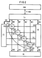
- processor elements PE0 to PE3 are provided.
- Each processor element PE can process a command independently, ie has the usual units that are required for command processing.
- Each processor element PE is connected to an instruction system IU via instruction buses IB0 to IB3.
- instruction buses IB0 to IB3 There is also a data bus DB0 to DB3 with a cache memory device CA, which is connected in a conventional manner to the main memory MM via a bus PI-MM.
- the cache memory device can contain a multiport cache memory, but it would also be possible to provide a separate cache memory for each processor element PE.
- a control memory CS must be provided for the micro-programs of the processor elements PE.
- each processor element PE would then be connected to the control memory CS via a separate bus MI0 to MI3.
- the control memory CS could in turn be implemented as a multiport control memory or a separate control memory could be provided for each processor element PE.
- the processor elements PE0 to PE3 could be connected via separate buses RB0 to RB3 to a register bank RG, which can be implemented as a multiport register bank.
- the instruction mechanism IU can be connected to the cache memory device CA via a data bus DBI and to the register bank RG via a bus RBI.
- the instructions of a program to be processed can be transmitted from the cache memory device CA in the usual way via the bus DBI to the instruction system IU.
- a command counter IC can be present in the command unit IU in a known manner.
- the commands are decoded there and are then distributed separately to the individual processor elements PE0 to PE3 via the command buses IBo to IB3. Since the processor elements PE can work independently of one another, it is possible for four instructions to be processed simultaneously in the exemplary embodiment.
- the data required for processing the commands are fetched from the cache memory device CA by the processor elements PE0 to PE3 via the data buses DB0 to DB3 in a conventional manner, or processed data are transferred to the cache memory device CA via the data buses DB.
- Register accesses required for the execution of the command take place via register buses RB0 to RB3 to register bank RG. If the processor elements PE are micro-programmed, then micro-programs that are in the control memory CS and are transferred from there via the micro-instruction buses MI0 to MI3 to the assigned processor elements are required for processing the commands, unless a separate control memory is provided for each processor element.
- Programs with a constant command length can be processed in parallel with the processor. It is advantageous if the command width is equal to or less than the word width.
- the processor is also expedient, but the instruction sequence IU must always correctly select and align the instruction sequence dynamically to the processor elements PE.
- the processor elements PE are always supplied with a set of instructions in parallel. These commands become parallel carried out, unless this is prevented by conflict situations.
- the order and thus the priority for processing the commands in conflict situations is given in the exemplary embodiment from left to right, that is to say from PE0 with the highest priority to PE3 with the lowest priority.
- the distribution of priorities can also be done differently; however, it must always be done in the order of the command sequence.
- processor elements PE it is also possible for the processor elements PE to be supplied with a new command dynamically, ie whenever possible. Then the priority of the command processing rotates with the command completion. So if e.g. the processor element PE1 is already finished with its command processing while the remaining processor elements PE0, PE2, PE3 are still active, then the processor element PE2 could receive the highest command processing priority and PE1 could already be supplied with a new command, etc.
- the instruction system IU can generate a disable signal for the processor elements that are not required and put them in the waiting state. This can e.g. also via so-called NOOP commands.
- conflict situations can be recognized when register results are calculated in parallel with the use of the results or when operands are processed in parallel with the results from operand processing.
- the forwarding of conflict signals K to the low-priority processor elements is shown symbolically in FIG. 2.
- a processor element PE detects, for example, the processor element PE0 that it is processing a command that, for example, requires write access to the cache device or to the register bank and can thus generate a conflict situation
- the processor element PE0 issues a conflict signal KO1 to the low-priority processor element PE1 and to all lower-priority ones Process elements PE2, PE3.
- These processor elements must then wait until their command has been processed if they use the same resource as PE0 until the higher-priority processor element has finished processing its command and the conflict signal KO1 has thus disappeared.
- the conflict signals can be transmitted to the processor elements, for example, via a bus.
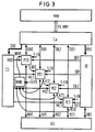
- the processor is expanded by a multiplexer KM0.
- This multiplexer KM0 can be used to determine which conflict signal K of a higher priority processor element is to be transmitted to the processor element PE0.
- the multiplexer KM0 e.g. A switching signal S-EN is supplied by the IU control unit.
- S-EN is supplied by the IU control unit.
- multiplexers KM1 and KM2 are provided, which allow the processor elements PE0 and PE1 to be supplied with conflict signals from other processor elements that can be selected by the multiplexers.
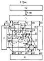
- the architecture of the Figure 4 is useful when conditional commands are to be executed. With conditional jump instructions, with conditional procedure calls and conditional jumps back with loop commands, two alternatives can be considered as a program continuation. Depending on the condition of the conditional command, either commands from a first branch or a second branch follow. In this case, the instructions of the two branches can be brought into the subsequent processor elements in parallel, thereby accelerating the execution of a program.
- processor element PE0 If, for example, such a conditional instruction is executed in processor element PE0, then the two following processor elements PE1 and PE2 could each be loaded with one instruction from a branch. Accordingly, the conflict signal of the processor element PE0 will be fed directly to the processor elements PE1 and PE2. The same applies if another processor element PE executes a conditional command. It can be seen in FIG. 4 that the conflict signals K of each processor element are each fed to two low-priority processor elements, the processor elements PE to which the conflict signal is fed being selectable via the multiplexers KM.
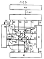
- a favorable solution also exists if an additional processor element is added for this situation or if the number of processor elements used is dynamic, if the lowest priority processor element is used for this, since it is more likely that it will not be used.
- This case is shown in FIG. 5, here the first command of the second branch is loaded into the processor element PE3 in the case of a conditional command. Accordingly, the conflict signal of the other processor elements is fed to the processor element PE3 via the multiplexer KM1.
- the processors shown in the figures contain units of known construction, e.g. an instruction mechanism IU, a cache memory CA, a control memory CS and a register bank RG and processor elements PE. There is therefore no need to go into the structure and function of these units.
Landscapes
- Engineering & Computer Science (AREA)
- Theoretical Computer Science (AREA)
- Software Systems (AREA)
- Physics & Mathematics (AREA)
- General Engineering & Computer Science (AREA)
- General Physics & Mathematics (AREA)
- Computer Hardware Design (AREA)
- Computing Systems (AREA)
- Multi Processors (AREA)
- Advance Control (AREA)
- Memory System Of A Hierarchy Structure (AREA)
Applications Claiming Priority (2)
| Application Number | Priority Date | Filing Date | Title |
|---|---|---|---|
| DE4030439 | 1990-09-26 | ||
| DE4030439 | 1990-09-26 |
Publications (2)
| Publication Number | Publication Date |
|---|---|
| EP0477597A2 true EP0477597A2 (fr) | 1992-04-01 |
| EP0477597A3 EP0477597A3 (en) | 1995-09-27 |
Family
ID=6415012
Family Applications (1)
| Application Number | Title | Priority Date | Filing Date |
|---|---|---|---|
| EP91114773A Withdrawn EP0477597A3 (en) | 1990-09-26 | 1991-09-02 | Method for parallel processing of programm instructions and processor to perform this process |
Country Status (2)
| Country | Link |
|---|---|
| EP (1) | EP0477597A3 (fr) |
| JP (1) | JPH04262452A (fr) |
Cited By (1)
| Publication number | Priority date | Publication date | Assignee | Title |
|---|---|---|---|---|
| EP0727738A3 (fr) * | 1995-02-14 | 1998-04-08 | Hal Computer Systems, Inc. | Circuit de contrÔle du déroulement d'instructions pour un microprocesseur superscalaire |
Family Cites Families (5)
| Publication number | Priority date | Publication date | Assignee | Title |
|---|---|---|---|---|
| US4809171A (en) * | 1984-06-20 | 1989-02-28 | Convex Computer Corporation | Concurrent processing of data operands |
| US4789925A (en) * | 1985-07-31 | 1988-12-06 | Unisys Corporation | Vector data logical usage conflict detection |
| US4903196A (en) * | 1986-05-02 | 1990-02-20 | International Business Machines Corporation | Method and apparatus for guaranteeing the logical integrity of data in the general purpose registers of a complex multi-execution unit uniprocessor |
| EP0312764A3 (fr) * | 1987-10-19 | 1991-04-10 | International Business Machines Corporation | Processeur de données comportant plusieurs unités d'exécution pour traiter plusieurs classes d'instructions en parallèle |
| US4969117A (en) * | 1988-05-16 | 1990-11-06 | Ardent Computer Corporation | Chaining and hazard apparatus and method |
-
1991
- 1991-09-02 EP EP91114773A patent/EP0477597A3/de not_active Withdrawn
- 1991-09-20 JP JP3268785A patent/JPH04262452A/ja not_active Withdrawn
Cited By (1)
| Publication number | Priority date | Publication date | Assignee | Title |
|---|---|---|---|---|
| EP0727738A3 (fr) * | 1995-02-14 | 1998-04-08 | Hal Computer Systems, Inc. | Circuit de contrÔle du déroulement d'instructions pour un microprocesseur superscalaire |
Also Published As
| Publication number | Publication date |
|---|---|
| EP0477597A3 (en) | 1995-09-27 |
| JPH04262452A (ja) | 1992-09-17 |
Similar Documents
| Publication | Publication Date | Title |
|---|---|---|
| DE69033065T2 (de) | Mehrfachbefehlsdecoder | |
| DE69032381T2 (de) | Vorrichtung und Verfahren für die kollektive Verzweigung in einem Mehrbefehlsstrommultiprozessor | |
| DE68929215T2 (de) | Datenprozessor | |
| EP0689694B1 (fr) | Procede de production automatique de groupes d'instructions pouvant etre traites de maniere parallele a partir d'un programme pour processeurs superscalaires | |
| DE60115982T2 (de) | Verfahren und Vorrichtung zum Zuordnen funktioneller Einheiten in einem Mehrfachthread-VLIM-Prozessor | |
| DE69130630T2 (de) | Synchrones Verfahren und Gerät für Prozessoren | |
| DE69127101T2 (de) | System für verteilte mehrfachrechnerkommunikation | |
| DE3750306T2 (de) | System zum Gewährleisten der logischen Unversehrtheit von Daten. | |
| DE3689394T2 (de) | Informationsverarbeitungsanlage mit einem Allzweckprozessor und einem Sonderzweckprozessor. | |
| DE3750935T2 (de) | Verfahren und System zum Erleichtern der Befehlsausführung in einem digitalen Rechner. | |
| DE3851488T2 (de) | Registerverwaltungssystem mit Ausführung von Befehlen in Unordnung in einem Computerprozessor. | |
| DE68921906T2 (de) | Verfahren für ein Multiprozessorsystem mit sich selbst zuordnenden Prozessoren. | |
| DE19914210B4 (de) | Verfahren und Prozessor für eine gestaffelte Ausführung einer Anweisung | |
| DE3586603T2 (de) | Datenprozessor fuer interpretierende und kompilierte sprache. | |
| DE3638572C2 (fr) | ||
| DE69133571T2 (de) | Datenprozessor mit der Fähigkeit, zwei Befehle gleichzeitig auszuführen | |
| DE2411963B2 (de) | Datenverarbeitungsanlage | |
| DE2847934A1 (de) | Datenverarbeitungseinrichtung mit einem mikrobefehlsspeicher | |
| DE69130757T2 (de) | Ausführungsvorrichtung für bedingte Verzweigungsbefehle | |
| DE2243956A1 (de) | Speicherprogrammierte datenverarbeitungsanlage | |
| DE19506435A1 (de) | Verfahren und Einrichtung zum Vermeiden von Rückschreibkonflikten zwischen einen gemeinsamen Rückschreibpfad verwendenden Ausführungseinheiten | |
| DE3855524T2 (de) | Arithmetik-Parallelverarbeitungseinheit und zugehöriger Kompilator | |
| DE1549474B2 (de) | Anordnung in einer elektronischen digitalen Datenverarbeitungsanlage zur Ausführung eines ersten Befehls und gleichzeitigen Decodierung eines folgenden Befehls | |
| DE69322566T2 (de) | Datenprozessor | |
| DE2533737A1 (de) | Datenprozessor |
Legal Events
| Date | Code | Title | Description |
|---|---|---|---|
| PUAI | Public reference made under article 153(3) epc to a published international application that has entered the european phase |
Free format text: ORIGINAL CODE: 0009012 |
|
| AK | Designated contracting states |
Kind code of ref document: A2 Designated state(s): AT DE ES FR GB IT NL |
|
| PUAL | Search report despatched |
Free format text: ORIGINAL CODE: 0009013 |
|
| STAA | Information on the status of an ep patent application or granted ep patent |
Free format text: STATUS: THE APPLICATION IS DEEMED TO BE WITHDRAWN |
|
| 18D | Application deemed to be withdrawn |
Effective date: 19950401 |
|
| AK | Designated contracting states |
Kind code of ref document: A3 Designated state(s): AT DE ES FR GB IT NL |