EP0477518A1 - Vorrichtung zum Ein-und/oder Auskoppeln von Licht für Monomode-Lichtwellenleiter - Google Patents
Vorrichtung zum Ein-und/oder Auskoppeln von Licht für Monomode-Lichtwellenleiter Download PDFInfo
- Publication number
- EP0477518A1 EP0477518A1 EP91113533A EP91113533A EP0477518A1 EP 0477518 A1 EP0477518 A1 EP 0477518A1 EP 91113533 A EP91113533 A EP 91113533A EP 91113533 A EP91113533 A EP 91113533A EP 0477518 A1 EP0477518 A1 EP 0477518A1
- Authority
- EP
- European Patent Office
- Prior art keywords
- coupling
- core
- optical
- optical waveguide
- light
- Prior art date
- Legal status (The legal status is an assumption and is not a legal conclusion. Google has not performed a legal analysis and makes no representation as to the accuracy of the status listed.)
- Granted
Links
- 230000008878 coupling Effects 0.000 title claims description 27
- 238000010168 coupling process Methods 0.000 title claims description 27
- 238000005859 coupling reaction Methods 0.000 title claims description 27
- 230000003287 optical effect Effects 0.000 claims abstract description 46
- 239000013307 optical fiber Substances 0.000 claims description 23
- 239000000835 fiber Substances 0.000 claims description 13
- 230000003760 hair shine Effects 0.000 claims 1
- 238000005452 bending Methods 0.000 abstract description 6
- 230000000694 effects Effects 0.000 abstract description 3
- 230000005855 radiation Effects 0.000 description 10
- 238000009826 distribution Methods 0.000 description 4
- 238000004519 manufacturing process Methods 0.000 description 4
- 238000003780 insertion Methods 0.000 description 2
- 230000037431 insertion Effects 0.000 description 2
- 230000005693 optoelectronics Effects 0.000 description 2
- 230000007704 transition Effects 0.000 description 2
- 230000006978 adaptation Effects 0.000 description 1
- 239000000853 adhesive Substances 0.000 description 1
- 230000001070 adhesive effect Effects 0.000 description 1
- 230000003321 amplification Effects 0.000 description 1
- 238000005253 cladding Methods 0.000 description 1
- 230000007423 decrease Effects 0.000 description 1
- 238000011161 development Methods 0.000 description 1
- 230000018109 developmental process Effects 0.000 description 1
- 238000005516 engineering process Methods 0.000 description 1
- 239000011159 matrix material Substances 0.000 description 1
- 230000008018 melting Effects 0.000 description 1
- 238000002844 melting Methods 0.000 description 1
- 238000003199 nucleic acid amplification method Methods 0.000 description 1
- 230000010287 polarization Effects 0.000 description 1
- 235000019353 potassium silicate Nutrition 0.000 description 1
- 239000004065 semiconductor Substances 0.000 description 1
- 239000000758 substrate Substances 0.000 description 1
Images

Classifications
-
- G—PHYSICS
- G02—OPTICS
- G02B—OPTICAL ELEMENTS, SYSTEMS OR APPARATUS
- G02B6/00—Light guides; Structural details of arrangements comprising light guides and other optical elements, e.g. couplings
- G02B6/24—Coupling light guides
- G02B6/26—Optical coupling means
- G02B6/262—Optical details of coupling light into, or out of, or between fibre ends, e.g. special fibre end shapes or associated optical elements
-
- G—PHYSICS
- G02—OPTICS
- G02B—OPTICAL ELEMENTS, SYSTEMS OR APPARATUS
- G02B6/00—Light guides; Structural details of arrangements comprising light guides and other optical elements, e.g. couplings
- G02B6/10—Light guides; Structural details of arrangements comprising light guides and other optical elements, e.g. couplings of the optical waveguide type
- G02B6/12—Light guides; Structural details of arrangements comprising light guides and other optical elements, e.g. couplings of the optical waveguide type of the integrated circuit kind
- G02B6/122—Basic optical elements, e.g. light-guiding paths
- G02B6/1228—Tapered waveguides, e.g. integrated spot-size transformers
-
- G—PHYSICS
- G02—OPTICS
- G02B—OPTICAL ELEMENTS, SYSTEMS OR APPARATUS
- G02B6/00—Light guides; Structural details of arrangements comprising light guides and other optical elements, e.g. couplings
- G02B6/24—Coupling light guides
- G02B6/42—Coupling light guides with opto-electronic elements
- G02B6/4201—Packages, e.g. shape, construction, internal or external details
- G02B6/4219—Mechanical fixtures for holding or positioning the elements relative to each other in the couplings; Alignment methods for the elements, e.g. measuring or observing methods especially used therefor
- G02B6/4236—Fixing or mounting methods of the aligned elements
- G02B6/424—Mounting of the optical light guide
Definitions
- the invention relates to a device for decoupling a fraction of the light power carried by a single-mode optical fiber or for coupling light power into a single-mode optical fiber.
- Couplers in which two fiber optic ends are polished at 45 ° to the fiber optic axis, coated with a dielectric interference mirror and aligned, based on the partial reflection of light waves on dielectric multilayers.
- Bending couplers which are based on the effect that a fiber emits light output during strong bending (see e.g. DE 39 04 662 A1).
- the invention has for its object to provide a device for coupling and / or coupling light for single-mode optical fibers, with which it is possible to couple or couple light with high efficiency.
- the device according to the invention is based on the effect that e.g. at the junction between two optical fibers with different core dimensions Core diameters in the case of fibers are emitted due to the mismatching of the fields when the change in the core dimensions occurs abruptly or steadily but very quickly, that is to say not gradually without radiation losses.
- the problem of radiation from a jump in dimensions is theoretically described in Neumann and Opielka, "Scattering matrix and radiation characteristics of the junction between two different monomode microwave or optical dielectric waveguides", Quantum Electron, 9 (1977), 209 and Opielka, " Radiation characteristics of a step discontinuity in a monomode optical fiber ", electron. Lett. 13 (1977), 319.
- the two publications contain equations which make it possible to calculate the relative radiated power and the directional characteristic of the radiation for both directions of propagation of the optical waveguide wave.
- a jump in the dimensions of single-mode optical fibers is used, e.g. B. a cross-sectional jump between different core diameters of fibers to couple light in and / or out.
- a wave is emitted predominantly in the direction of propagation of the wave guided in the optical waveguide.
- This can be detected with an optical receiver, which is arranged, for example, in a ring around the optical waveguide in the region of the emitted wave.
- the ring-shaped arrangement is useful if you want to receive the emitted wave with little loss.
- the coupling in of light with an annular transmitter surrounding the optical waveguide can also take place. It is also possible to couple light in and out at the same time.
- the invention provides a simple, inexpensive to manufacture and effective device for coupling and decoupling light from or into a single-mode optical waveguide.
- the device is simpler and cheaper to manufacture than directional couplers and mirror couplers.
- Compared to the bending coupler it has the advantage that the optical waveguide does not have to be bent and thus the risk of the optical waveguide breaking is avoided.
- a higher coupling efficiency can be achieved with fibers.
- the device can be spliced into a fiber in a simple manner with the aid of conventional splicing devices with a negligibly low insertion loss.
- the degree of coupling can be set very easily by appropriately dimensioning the core-radius ratio from very small values to close to 100%. The degree of coupling increases slowly with the wavelength. The device is thus intrinsically broadband.
- Fig. 1 shows in longitudinal section the boundary between core 1 and cladding 2 of a single-mode optical fiber.
- the cross-section of the core 1 is initially constant (from left to right), then suddenly decreases (cross-sectional jump 3), then gradually increases again (taper 4) until the initial diameter is reached again.
- a guided wave W spreads from left to right.
- the field diameter of the basic mode in the optical waveguide with the larger core diameter in front of the cross-sectional jump 3 is smaller than the field diameter of the basic mode in the optical waveguide with the smaller core diameter immediately behind the cross-sectional jump 3 AW, which is schematically represented by the two oblique light rays drawn in.
- the radiation is mainly in the forward direction at small angles to the fiber optic axis.
- the power of the basic mode reflected at the cross-section jump 3 and the power of the wave radiated in the reverse direction are practically negligible. If the wave guided in the optical waveguide passes through a combination of cross-sectional jump 3 and taper 4 in the opposite direction, the same fraction of the power is emitted. The radiation again takes place predominantly in the forward direction at small angles against the optical waveguide axis, as is shown schematically in FIG. 2 by the two obliquely running light beams. In reciprocal media, each light wave can be reversed in its direction of propagation. Therefore, at the location of a cross-sectional jump 3, light can also be coupled into an optical waveguide from the outside (FIGS. 3 and 4).
- an incident wave EW is shown schematically by two light rays inclined at an angle to the optical fiber axis.
- a coupled-in wave We is generated, which propagates in the optical waveguide.
- the field distribution in the incident wave EW must match the field distribution of the wave AW radiated at the cross-sectional jump as well as possible with regard to the shape of the wave front, transverse intensity distribution and polarization.
- the problem of connecting the optical receiver or transmitter to the coupler can be solved in various ways.
- an optical waveguide is guided through a large-area semiconductor photodiode 5 provided with a bore.
- the diameter of the hole must be slightly larger than the individual diameter of the optical fiber.
- most of the photons emitted by the cross-sectional jump 3 fall on the photosensitive surface of the photodiode, and the coupling efficiency is therefore high.
- This solution appears to be particularly advantageous if the photodiode 5 is part of an integrated optoelectronic circuit.
- a hole must then be drilled through the substrate. To connect the optical fiber, it is sufficient to pull the optical fiber through the hole and with a transparent adhesive to be permanently connected to the integrated optoelectronic circuit.
- the photodiode in FIG. 5 can be replaced by a luminescent diode (LED) provided with a bore.
- LED luminescent diode
- the optical waveguide through a perforated plane mirror 6 set up at an angle of, for example, 45 ° to the optical waveguide axis and to couple light into the optical waveguide by means of lateral light radiation.
- Decoupling can also be done with the help of a pierced plane mirror. If a concave mirror is used instead of the plane mirror, the coupled or uncoupled shaft can be focused at the same time.
- the adjustment of the field distributions required for effective coupling can be achieved with the help of lens systems and phase plates.
- a continuous but very rapid change in the core diameter which is not adiabatic, can also be used in the device according to the invention.
- a long adiabatic biconical taper can first be produced in a known manner by melting and pulling an optical waveguide, in which the jacket diameter in the waist is reduced from the standard value, for example, to half the value.
- a fiber optic end surface is prepared by bending, pulling and breaking.
- the thinner end of the taper is then spliced to one end of an optical fiber with a normal core diameter. Due to the surface tension of the liquid glass, the optical fiber axes are automatically aligned.
Landscapes
- Physics & Mathematics (AREA)
- General Physics & Mathematics (AREA)
- Optics & Photonics (AREA)
- Engineering & Computer Science (AREA)
- Power Engineering (AREA)
- Microelectronics & Electronic Packaging (AREA)
- Optical Couplings Of Light Guides (AREA)
- Optical Integrated Circuits (AREA)
- Optical Communication System (AREA)
Abstract
Description
- Die Erfindung betrifft eine Vorrichtung zum Auskoppeln eines Bruchteils der von einem Monomode-Lichtwellenleiter geführten Lichtleistung bzw. zum Einkoppeln von Lichtleistung in einen Monomode-Lichtwellenleiter.
- In der optischen Nachrichtentechnik besteht häufig das Problem, einen Teil der in einem durchgehenden Lichtwellenleiter geführten Leistung auszukoppeln, z. B. zur Regelung der Laserleistung, zur Regelung der Verstärkung von optischen Verstärkern, zur optimalen Ausrichtung einer sekundären Faser bei der Herstellung einer Schmelz-Spleißverbindung, zum Anschluß der Empfänger vieler Teilnehmer an ein Lichtwellenleiternetz mit Bus-, Ring- oder Baumstruktur, usw. Umgekehrt besteht auch oft das Problem, Licht mit hohem Wirkungsgrad in einen durchgehenden Lichtwellenleiter einzukoppeln, z. B. um die Einfügungsdämpfung einer Faserverbindung zu minimieren oder um die optischen Sender vieler Teilnehmer an ein Lichtwellenleiternetz anzuschließen. Diese Probleme bestehen sowohl bei der Verwendung optischer Fasern als auch bei planaren Lichtwellenleitern.
- Es sind bereits mehrere Koppelvorrichtungen bekannt, die auf verschiedenen physikalischen Prinzipien beruhen:
- Richtkoppler nach dem Prinzip des Schmelzkopplers oder nach dem Prinzip des seitlich polierten Lichtwellenleiters, die auf der Verkopplung der Grundmoden in zwei parallelen, dicht benachbarten dielektrischen Leitungen beruhen.
- Koppler bei denen zwei Lichtwellenleiterenden unter 45° zur Lichtwellenleiterachse poliert, mit einem dielektrischen Interferenzspiegel beschichtet und fluchtend zusammengefügt sind, die auf der partiellen Reflektion von Lichtwellen an dielektrischen Mehrfachschichten beruhen.
- Biegekoppler, die auf dem Effekt beruhen, daß eine Faser bei starkem Biegen Lichtleistung abstrahlt (siehe z.B. DE 39 04 662 A1).
- Die Herstellung von Richtkopplern und Spiegelkopplern ist aufwendig. Bei Biegekopplern ist es schwierig, Lichtleistung effektiv einzukoppeln. Um stark anzukoppeln, muß man außerdem den Lichtwellenleiter stark krümmen, so daß die Gefahr eines sofortigen oder späteren Lichtwellenleiterbruches besteht.
- Der Erfindung liegt die Aufgabe zugrunde, eine Vorrichtung zum Ein- und/oder Auskoppeln von Licht für Monomode-Lichtwellenleiter anzugeben, mit der es möglich ist, Licht mit hohem Wirkungsgrad aus- bzw. einzukoppeln.
- Die Aufgabe wird gelöst mit einer Vorrichtung mit den Merkmalen des Patentanspruches 1. Vorteilhafte Weiterbildungen sind in den Unteransprüchen angegeben.
- Erfindungsgemäß wird eine Vorrichtung zum Ein- und/oder Auskoppeln von Licht für Monomode-Lichtwellenleiter mit den folgenden Merkmalen angegeben:
- - Die Vorrichtung weist eine sprungartige abrupte oder stetige, sehr rasche Änderung des Kerndurchmessers von einem ersten größeren in einen zweiten kleineren Kerndurchmesser auf.
- - An die sprungartige oder stetige, sehr rasche Änderung des Kerndurchmessers schließt sich eine langsame nahezu verlustfreie Anpassung des Kerndurchmesser vom zweiten kleineren bis zu einem dritten Kerndurchmesser an, wobei der dritte Kerndurchmesser dem ersten Kerndurchmesser entsprechen kann.
- - Ein optisches Element umgibt den Lichtwellenleiter und dient zur Ein- und/oder Auskopplung von Licht.
- Die Vorrichtung gemäß der Erfindung beruht auf dem Effekt, daß an der Verbindungsstelle zwischen zwei Lichtwellenleitern mit verschiedenen Kernabmessungen z.B. Kerndurchmessern bei Fasern aufgrund der Fehlanpassung der Felder Lichtleistung abgestrahlt wird, wenn die Änderung der Kernabmessungen sprungartig abrupt oder stetig aber sehr rasch, also nicht allmählich ohne Abstrahlungsverluste erfolgt. Das Problem der Abstrahlung von einem Sprung in den Abmessungen ist theoretisch in Neumann und Opielka, "Scattering matrix and radiation characteristics of the junction between two different monomode microwave or optical dielectric waveguides", Quantum Electron, 9(1977), 209 und Opielka, "Radiation characteristics of a step discontinuity in a monomode optical fibre", Electron. Lett. 13(1977), 319 analysiert worden. Die beiden Veröffentlichungen enthalten Gleichungen, die es gestatten, die relative abgestrahlte Leistung und die Richtcharakteristik der Strahlung für beide Ausbreitungsrichtungen der Lichtwellenleiterwelle zu berechnen.
- Erfindungsgemäß wird ein Sprung in den Abmessungen von Monomode-Lichtwellenleitern ausgenutzt, z. B. ein Querschnittssprung zwischen unterschiedlichen Kerndurchmessern von Fasern, um Licht ein- und/oder auszukoppeln. Hinter dem Sprung wird vorwiegend in der Ausbreitungsrichtung der im Lichtwellenleiter geführten Welle eine Welle abgestrahlt. Diese kann mit einen optischen Empfänger detektiert werden, der beispielsweise ringförmig um den Lichtwellenleiter im Bereich der abgestrahlten Welle angeordnet wird. Die ringförmige Anordnung ist sinnvoll, wenn man die abgestrahlte Welle mit geringen Verlusten empfangen will. Analog zum Auskoppeln kann auch das Einkoppeln von Licht mit einem ringförmigen, den Lichtwellenleiter umgebenden Sender erfolgen. Auch das gleichzeitige Ein- und Auskoppeln von Licht ist möglich. Damit sich die Koppelvorrichtung für Fasern einfach in einen normalen Lichtwellenleiter einspleißen läßt, ist es zweckmäßig, hinter dem Querschnittssprung den Kernradius sehr langsam wieder auf den ursprünglichen Wert anwachsen zu lassen. Bei einem solchen Übergang (Taper) wird die Grundmode im Lichtwellenleiter mit verringertem Kerndurchmesser ohne Strahlungsverluste in die Grundmode in dem Lichtwellenleiter mit normalem Kerndurchmesser transformiert. Ein solcher Übergang ist aus der DE 30 12 775 C2 bekannt. Die Abstrahlung ist dabei sehr gering.
- Durch die Erfindung wird eine einfache, billig herstellbare und wirksame Vorrichtung zur Aus-und Einkopplung von Licht aus einem bzw. in einen Monomode-Lichtwellenleiter angegeben. Die Vorrichtung ist einfacher und billiger herzustellen als Richtkoppler und Spiegelkoppler. Gegenüber dem Biegekoppler besitzt sie den Vorteil, daß der Lichtwellenleiter nicht gebogen werden muß und somit die Gefahr des Lichtwellenleiterbruchs vermieden wird. Außerdem läßt sich bei Fasern wegen der wesentlich einfacheren Struktur des Feldes der abgestrahlten Welle (sphärische Wellenfronten, Intensität unabhängig von Azimutwinkel) ein höherer Einkoppelwirkungsgrad erzielen. Da der Lichtwellenleiter an beiden Enden der Vorrichtung Standardabmessungen aufweisen kann, läßt sich die Vorrichtung in einfacher Weise mit Hilfe üblicher Spleißgeräte mit verschwindend kleiner Einfügungsdämpfung in eine Faser einspleißen. Der Koppelgrad läßt sich durch passende Dimensionierung des Kern-Radien-Verhältnisses sehr einfach von sehr kleinen Werten bis nahe 100 % festeinstellen. Der Koppelgrad steigt mit der Wellenlänge nur langsam an. Die Vorrichtung ist also intrinsisch breitbandig.
- Anhand der Zeichnungen werden Ausführungsbeispiele der Erfindung beschrieben.
- Es zeigen:
- Fig. 1 und 2 je einen Längsschnitt durch eine erfindungsgemäße Vorrichtung mit abgestrahlter Welle,
- Fig. 3 und 4 je einen Längsschnitt durch eine erfindungsgemäße Vorrichtung mit eingestrahlter Welle,
- Fig. 5 eine Vorrichtung mit Empfänger und
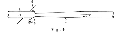
- Fig. 6 eine Vorrichtung mit Sender.
- Fig. 1 zeigt im Längsschnitt die Grenze zwischen Kern 1 und Mantel 2 eines Monomode-Lichtwellenleiters. Der Querschnitt des Kerns 1 ist (von links nach rechts) zunächst konstant, wird dann sprunghaft kleiner (Querschnittssprung 3), steigt dann allmählich wieder an (Taper 4), bis der Anfangsdurchmesser wieder erreicht ist. Eine geführte Welle W breitet sich von links nach rechts aus. Der Felddurchmesser der Grundmode in dem Lichtwellenleiter mit dem größeren Kerndurchmesser vor dem Querschnittssprung 3 ist kleiner als der Felddurchmesser der Grundmode in dem Lichtwellenleiter mit dem kleineren Kerndurchmesser unmittelbar hinter dem Querschnittssprung 3. Bedingt durch die Fehlanpassung der transversalen Feldverteilungen entsteht an dem Querschnittssprung 3 eine abgestrahlte Welle AW, die durch die beiden eingezeichneten schräg verlaufenden Lichtstrahlen schematisch dargestellt wird. Die Abstrahlung erfolgt vorwiegend in Vorwärtsrichtung unter kleinen Winkeln zur Lichtwellenleiterachse. Die Leistung der an dem Querschnittssprung 3 reflektierten Grundmode und die Leistung der in Rückrichtung abgestrahlten Welle sind praktisch vernachlässigbar. Wenn die im Lichtwellenleiter geführte Welle eine Kombination von Querschnittssprung 3 und Taper 4 in der entgegengesetzten Richtung durchläuft, wird der gleiche Bruchteil der Leistung abgestrahlt. Die Abstrahlung erfolgt wiederum vorwiegend in Vorwärtsrichtung unter kleinen Winkeln gegen die Lichtwellenleiterachse, wie es schematisch in Fig. 2 durch die beiden schräg verlaufenden Lichtstrahlen dargestellt wird. In reziproken Medien läßt sich jede Lichtwelle in ihrer Ausbreitungsrichtung umkehren. Daher läßt sich an der Stelle eines Querschnittssprungs 3 auch Licht von außen in einen Lichtwellenleiter einkoppeln (Fig. 3 und Fig. 4). In den Figuren 3 und 4 wird eine eingestrahlte Welle EW durch zwei schräg zur Lichtwellenleiterachse geneigte Lichtstrahlen schematisch dargestellt. Es wird eine eingekoppelte Welle We erzeugt, die sich im Lichtwellenleiter ausbreitet. Zur effektiven Einkopplung von Lichtleistung muß die Feldverteilung in der eingestrahlten Welle EW mit der Feldverteilung der am Querschnittssprung abgestrahlten Welle AW möglichst gut übereinstimmen hinsichlich Form der Wellenfront, transversaler Intensitätsverteilung und Polarisation.
- Das Problem der Verbindung von optischem Empfänger oder Sender mit dem Koppler kann auf verschiedene Weisen gelöst werden. In Fig. 5 ist ein Lichtwellenleiter durch eine mit einer Bohrung versehene großflächige Halbleiterphotodiode 5 geführt. Der Durchmesser der Bohrung muß etwas größer als der Einzeldurchmesser des Lichtwellenleiters sein. Bei hinreichend großem Abstand zwischen dem Kerndurchmessersprung 3 und der Photodiode 5 fallen die meisten der vom Querschnittssprung 3 abgestrahlten Photonen auf die lichtempfindliche Fläche der Photodiode und der Kopplungswirkungsgrad ist daher hoch. Besonders vorteilhaft erscheint diese Lösung, wenn die Photodiode 5 Teil einer integriert-optoelektronischen Schaltung ist. Durch das Substrat ist dann ein Loch zu bohren. Zur Ankopplung des Lichtwellenleiters genügt es, den Lichtwellenleiter durch die Bohrung zu ziehen und mit einem transparenten Klebstoff permanent mit der integriertoptoelektronischen Schaltung zu verbinden.
- Um Licht in einen Lichtwellenleiter einzukoppeln, kann man in Fig. 5 die Photodiode durch eine mit einer Bohrung versehene Lumineszenzdiode (LED) ersetzen.
- Wie in Fig. 6 dargestellt ist es auch möglich, den Lichtwellenleiter durch einen unter einem Winkel von beispielsweise 45° zur Lichtwellenleiterachse aufgestellten durchbohrten Planspiegel 6 zu führen und durch seitliche Lichteinstrahlung Licht in den Lichtwellenleiter einzukoppel. Auch eine Auskopplung kann mit Hilfe eines durchbohrten Planspiegels erfolgen. Verwendet man anstelle des Planspiegels einen Hohlspiegel, so läßt sich die ein- bzw. ausgekoppelte Welle gleichzeitig fokussieren. Die zur effektiven Einkopplung erforderliche Anpassung der Feldverteilungen läßt sich mit Hilfe von Linsensystemen und Phasenplatten erreichen.
- Anstelle einer abrupten Änderung des Kerndurchmessers kann man auch eine stetige, jedoch sehr rasche Änderung des Kerndurchmessers, die nicht adiabatisch ist, in der erfindungsgemäßen Vorrichtung verwenden.
- Kerndurchmessers, die nicht adiabatisch ist, in der erfindungsgemäßen Vorrichtung verwenden.
- Zur Herstellung einer erfindungsgemäßen Vorrichtung kann man zunächst in bekannter Weise durch Schmelzen und Ziehen eines Lichtwellenleiters einen langen adiabatischen bikonischen Taper herstellen, bei dem der Manteldurchmesser in der Taille von dem Normwert beispielsweise auf den halben Wert reduziert ist. In der Taille wird durch Biegen, Ziehen und Brechen eine Lichtwellenleiterendfäche präpariert. Danach wird das dünnere Taperende mit einem Ende eines Lichtwellenleiters mit normalem Kerndurchmesser verspleißt. Durch die Oberflächenspannung des flüssigen Glases werden die Lichtwellenleiterachsen dabei automatisch fluchtend ausgerichtet.
Claims (5)
Applications Claiming Priority (2)
| Application Number | Priority Date | Filing Date | Title |
|---|---|---|---|
| DE4028790 | 1990-09-11 | ||
| DE4028790A DE4028790C1 (de) | 1990-09-11 | 1990-09-11 |
Publications (2)
| Publication Number | Publication Date |
|---|---|
| EP0477518A1 true EP0477518A1 (de) | 1992-04-01 |
| EP0477518B1 EP0477518B1 (de) | 1995-03-08 |
Family
ID=6414023
Family Applications (1)
| Application Number | Title | Priority Date | Filing Date |
|---|---|---|---|
| EP91113533A Expired - Lifetime EP0477518B1 (de) | 1990-09-11 | 1991-08-13 | Vorrichtung zum Ein-und/oder Auskoppeln von Licht für Monomode-Lichtwellenleiter |
Country Status (3)
| Country | Link |
|---|---|
| EP (1) | EP0477518B1 (de) |
| AT (1) | ATE119679T1 (de) |
| DE (2) | DE4028790C1 (de) |
Cited By (1)
| Publication number | Priority date | Publication date | Assignee | Title |
|---|---|---|---|---|
| EP0539877A1 (de) * | 1991-10-30 | 1993-05-05 | Hughes Aircraft Company | Glasfaser mit inneren teildurchlässigen Spiegeln |
Families Citing this family (1)
| Publication number | Priority date | Publication date | Assignee | Title |
|---|---|---|---|---|
| DE4315846A1 (de) * | 1993-03-30 | 1994-10-06 | Sel Alcatel Ag | Faseroptischer Verstärker |
Citations (3)
| Publication number | Priority date | Publication date | Assignee | Title |
|---|---|---|---|---|
| US4475789A (en) * | 1981-11-09 | 1984-10-09 | Canadian Patents & Development Limited | Optical fiber power tap |
| GB2169096A (en) * | 1984-12-28 | 1986-07-02 | Int Standard Electric Corp | Joining optical fibres using numerical aperture transformer |
| DE3904662A1 (de) * | 1989-02-16 | 1990-08-23 | Licentia Gmbh | Faseroptische koppelanordnung |
Family Cites Families (2)
| Publication number | Priority date | Publication date | Assignee | Title |
|---|---|---|---|---|
| GB8603672D0 (en) * | 1986-02-14 | 1986-03-19 | British Telecomm | Reducing splice loss between dissimilar fibres |
| DE3806866C2 (de) * | 1988-03-03 | 1994-07-14 | Kabelmetal Electro Gmbh | Verfahren zum Verbinden von zwei optischen Fasern |
-
1990
- 1990-09-11 DE DE4028790A patent/DE4028790C1/de not_active Expired - Lifetime
-
1991
- 1991-08-13 DE DE59104861T patent/DE59104861D1/de not_active Expired - Fee Related
- 1991-08-13 AT AT91113533T patent/ATE119679T1/de active
- 1991-08-13 EP EP91113533A patent/EP0477518B1/de not_active Expired - Lifetime
Patent Citations (3)
| Publication number | Priority date | Publication date | Assignee | Title |
|---|---|---|---|---|
| US4475789A (en) * | 1981-11-09 | 1984-10-09 | Canadian Patents & Development Limited | Optical fiber power tap |
| GB2169096A (en) * | 1984-12-28 | 1986-07-02 | Int Standard Electric Corp | Joining optical fibres using numerical aperture transformer |
| DE3904662A1 (de) * | 1989-02-16 | 1990-08-23 | Licentia Gmbh | Faseroptische koppelanordnung |
Non-Patent Citations (2)
| Title |
|---|
| ELECTRONICS LETTERS Band 13, Nr. 11, Mai 1977, Seiten 319-321; D. OPIELKA: "Radiation characteristics of a step discontinuity in a monomode optical fibre" * |
| PATENT ABSTRACTS OF JAPAN Band 9, Nr. 177 (P-375)(1900), 23. Juli 1985; & JP - A - 60050504 (NIPPON DENKI) 20.03.1985 * |
Cited By (2)
| Publication number | Priority date | Publication date | Assignee | Title |
|---|---|---|---|---|
| EP0539877A1 (de) * | 1991-10-30 | 1993-05-05 | Hughes Aircraft Company | Glasfaser mit inneren teildurchlässigen Spiegeln |
| US5361383A (en) * | 1991-10-30 | 1994-11-01 | Hughes Aircraft Company | Optical fiber having internal partial mirrors and interferometer using same |
Also Published As
| Publication number | Publication date |
|---|---|
| DE59104861D1 (de) | 1995-04-13 |
| EP0477518B1 (de) | 1995-03-08 |
| DE4028790C1 (de) | 1992-02-06 |
| ATE119679T1 (de) | 1995-03-15 |
Similar Documents
| Publication | Publication Date | Title |
|---|---|---|
| DE3751674T2 (de) | Optischer Faserkoppler | |
| DE3687944T2 (de) | Kopplungselement fuer monomodefaser und dieses aufweisende uebertragungssystem. | |
| DE69030077T2 (de) | Methode zur Herstellung einer eine reflexionsarme faseroptische Verbindung enthaltenden optischen Vorrichtung | |
| GB1567701A (en) | Optical coupling devices | |
| EP0622649A1 (de) | Optischer Koppler mit Anzapfstelle | |
| DE69510406T2 (de) | Faseroptische Lichteinkopplungsschnittstelle mit vergrösserter Einfallsfläche | |
| DE2745940A1 (de) | Optisches schaltkreiselement | |
| US4431261A (en) | Fiber optic splitter | |
| DE102011085637B4 (de) | Optische Transportfaser und Verfahren zu deren Herstellung und Verfahren zum Verkleben | |
| US6467969B1 (en) | Article comprising a multimode optical fiber coupler | |
| EP0107840B1 (de) | Verfahren zum Herstellen einer optischen Koppelvorrichtung, insbesondere Verfahren zur Verminderung der Wandstärke von aus Quarzglas bestehenden Ummantelungen von Lichtwellenleiter-Glasfasern | |
| DE2409455A1 (de) | Auskoppelvorrichtung fuer licht aus optischen wellenleitern | |
| DE68929169T2 (de) | Durchbruchsfreier optischer Koppler | |
| DE2905916A1 (de) | Faseroptische uebertragungsvorrichtung | |
| DE102022102057B4 (de) | Lichtwellenleiterstecker sowie Lichtwellenleiterverbinder mit einem solchen | |
| EP0477518B1 (de) | Vorrichtung zum Ein-und/oder Auskoppeln von Licht für Monomode-Lichtwellenleiter | |
| EP0499066B1 (de) | Faseroptischer Verstärker | |
| EP0301388B1 (de) | Reflektionssender für ein bidirektionales LWL-Kommunikationssystem | |
| DE69709330T2 (de) | Wellenleiter-photodetektoranschluss | |
| DE3741284C2 (de) | Faseroptischer Mehrfachkoppler | |
| DE10314495B3 (de) | Optische Koppeleinheit | |
| DE102023118609B4 (de) | Multilichtwellenleiterstecker sowie Lichtwellenleiterverbinder mit einem solchen | |
| DE3908530C1 (de) | ||
| DE2348924A1 (de) | Einkoppler und speiseverfahren fuer dielektrische lichtwellenleiter | |
| DE2931530A1 (de) | Anordnung zur auskopplung von licht aus einer lichtleitfaser-uebertragungsstrecke |
Legal Events
| Date | Code | Title | Description |
|---|---|---|---|
| PUAI | Public reference made under article 153(3) epc to a published international application that has entered the european phase |
Free format text: ORIGINAL CODE: 0009012 |
|
| AK | Designated contracting states |
Kind code of ref document: A1 Designated state(s): AT CH DE FR GB LI |
|
| 17P | Request for examination filed |
Effective date: 19920219 |
|
| 17Q | First examination report despatched |
Effective date: 19940127 |
|
| GRAA | (expected) grant |
Free format text: ORIGINAL CODE: 0009210 |
|
| AK | Designated contracting states |
Kind code of ref document: B1 Designated state(s): AT CH DE FR GB LI |
|
| REF | Corresponds to: |
Ref document number: 119679 Country of ref document: AT Date of ref document: 19950315 Kind code of ref document: T |
|
| REF | Corresponds to: |
Ref document number: 59104861 Country of ref document: DE Date of ref document: 19950413 |
|
| ET | Fr: translation filed | ||
| GBT | Gb: translation of ep patent filed (gb section 77(6)(a)/1977) |
Effective date: 19950614 |
|
| PLBE | No opposition filed within time limit |
Free format text: ORIGINAL CODE: 0009261 |
|
| STAA | Information on the status of an ep patent application or granted ep patent |
Free format text: STATUS: NO OPPOSITION FILED WITHIN TIME LIMIT |
|
| 26N | No opposition filed | ||
| PGFP | Annual fee paid to national office [announced via postgrant information from national office to epo] |
Ref country code: DE Payment date: 19960424 Year of fee payment: 5 |
|
| PGFP | Annual fee paid to national office [announced via postgrant information from national office to epo] |
Ref country code: GB Payment date: 19960729 Year of fee payment: 6 |
|
| PGFP | Annual fee paid to national office [announced via postgrant information from national office to epo] |
Ref country code: FR Payment date: 19960814 Year of fee payment: 6 |
|
| PGFP | Annual fee paid to national office [announced via postgrant information from national office to epo] |
Ref country code: AT Payment date: 19960820 Year of fee payment: 6 |
|
| PGFP | Annual fee paid to national office [announced via postgrant information from national office to epo] |
Ref country code: CH Payment date: 19960823 Year of fee payment: 6 |
|
| PG25 | Lapsed in a contracting state [announced via postgrant information from national office to epo] |
Ref country code: DE Effective date: 19970501 |
|
| PG25 | Lapsed in a contracting state [announced via postgrant information from national office to epo] |
Ref country code: GB Free format text: LAPSE BECAUSE OF NON-PAYMENT OF DUE FEES Effective date: 19970813 Ref country code: AT Free format text: LAPSE BECAUSE OF NON-PAYMENT OF DUE FEES Effective date: 19970813 |
|
| PG25 | Lapsed in a contracting state [announced via postgrant information from national office to epo] |
Ref country code: LI Free format text: LAPSE BECAUSE OF NON-PAYMENT OF DUE FEES Effective date: 19970831 Ref country code: CH Free format text: LAPSE BECAUSE OF NON-PAYMENT OF DUE FEES Effective date: 19970831 |
|
| GBPC | Gb: european patent ceased through non-payment of renewal fee |
Effective date: 19970813 |
|
| REG | Reference to a national code |
Ref country code: CH Ref legal event code: PL |
|
| PG25 | Lapsed in a contracting state [announced via postgrant information from national office to epo] |
Ref country code: FR Free format text: LAPSE BECAUSE OF NON-PAYMENT OF DUE FEES Effective date: 19980430 |
|
| REG | Reference to a national code |
Ref country code: FR Ref legal event code: ST |