EP0477504A1 - Reduction of foreign particulate matter on semiconductor wafers - Google Patents
Reduction of foreign particulate matter on semiconductor wafers Download PDFInfo
- Publication number
- EP0477504A1 EP0477504A1 EP91112984A EP91112984A EP0477504A1 EP 0477504 A1 EP0477504 A1 EP 0477504A1 EP 91112984 A EP91112984 A EP 91112984A EP 91112984 A EP91112984 A EP 91112984A EP 0477504 A1 EP0477504 A1 EP 0477504A1
- Authority
- EP
- European Patent Office
- Prior art keywords
- solution
- particulate matter
- acid
- fluorine
- foreign particulate
- Prior art date
- Legal status (The legal status is an assumption and is not a legal conclusion. Google has not performed a legal analysis and makes no representation as to the accuracy of the status listed.)
- Withdrawn
Links
Classifications
-
- H—ELECTRICITY
- H01—ELECTRIC ELEMENTS
- H01L—SEMICONDUCTOR DEVICES NOT COVERED BY CLASS H10
- H01L21/00—Processes or apparatus adapted for the manufacture or treatment of semiconductor or solid state devices or of parts thereof
- H01L21/02—Manufacture or treatment of semiconductor devices or of parts thereof
- H01L21/02041—Cleaning
- H01L21/02043—Cleaning before device manufacture, i.e. Begin-Of-Line process
- H01L21/02052—Wet cleaning only
-
- Y—GENERAL TAGGING OF NEW TECHNOLOGICAL DEVELOPMENTS; GENERAL TAGGING OF CROSS-SECTIONAL TECHNOLOGIES SPANNING OVER SEVERAL SECTIONS OF THE IPC; TECHNICAL SUBJECTS COVERED BY FORMER USPC CROSS-REFERENCE ART COLLECTIONS [XRACs] AND DIGESTS
- Y10—TECHNICAL SUBJECTS COVERED BY FORMER USPC
- Y10S—TECHNICAL SUBJECTS COVERED BY FORMER USPC CROSS-REFERENCE ART COLLECTIONS [XRACs] AND DIGESTS
- Y10S438/00—Semiconductor device manufacturing: process
- Y10S438/906—Cleaning of wafer as interim step
-
- Y—GENERAL TAGGING OF NEW TECHNOLOGICAL DEVELOPMENTS; GENERAL TAGGING OF CROSS-SECTIONAL TECHNOLOGIES SPANNING OVER SEVERAL SECTIONS OF THE IPC; TECHNICAL SUBJECTS COVERED BY FORMER USPC CROSS-REFERENCE ART COLLECTIONS [XRACs] AND DIGESTS
- Y10—TECHNICAL SUBJECTS COVERED BY FORMER USPC
- Y10S—TECHNICAL SUBJECTS COVERED BY FORMER USPC CROSS-REFERENCE ART COLLECTIONS [XRACs] AND DIGESTS
- Y10S438/00—Semiconductor device manufacturing: process
- Y10S438/974—Substrate surface preparation
Definitions
- This invention relates to the cleaning of surfaces, and, more particularly, to an improved method of reducing foreign particulate matter on surfaces of semiconductor wafers.
- cleaning steps are performed before or after various steps to remove foreign contaminants or impurities from the surfaces of semiconductor wafers.
- wafers are commonly polished with abrasive slurries to produce smooth, polished surfaces; after polishing, it is necessary to remove the slurry and other surface contaminants from the wafers. Removal of foreign particulate matter, such as metallics and organic contaminants, is also required prior to high temperature processing steps, such as diffusion, thermal oxidation and epitaxial growth; otherwise, these impurities can adversely affect surface stability, reliability, electrical performance and production yield of devices.
- Cleaning steps are also commonly carried out after stripping photoresist materials from the surfaces of wafers and following etching steps.
- the surface to be treated is contacted with a solution comprising a strong acid and a very small amount of a fluorine-containing compound, which is effective in reducing foreign particulate matter contamination, without significant etching, of the surface.
- a solution which further contains an oxidizing agent, such as hydrogen peroxide, and in which the fluorine-containing compound is hydrofluoric acid.
- the solution employed according to the invention comprises a strong acid and a very small amount of a fluorine-containing compound.
- Any suitable strong acid can be employed, such as sulfuric acid, nitric acid and trifluoracetic acid, although sulfuric acid is preferred.
- a particularly preferred fluorine-containing compound is hydrofluoric acid.
- a very small amount of the fluorine-containing compound is employed. This amount is effective in reducing foreign particulate matter contamination of the surface being treated, but without significant etching of the surface. Without being bound by theory, it is believed that this is accomplished by establishing a chemophobic surface upon contacting the surface with the solution, in contrast with a chemophilic surface.
- a chemophilic surface is formed, with a residual film of the solution remaining on the surface.
- Foreign particulate matter from the solution is essentially trapped by the residual film on the surface being cleaned.
- These particulate contaminants once on the surface resist removal with cleaning solutions ordinarily employed by those skilled in the art. It is believed, however, that the method of the invention provides a chemophobic condition on the surface, where no observable residual film of the solution remains, although tiny droplets may still be present. With this condition, the solution and particulate contaminants are allowed to drain, thus producing a haze-free surface.
- the fluorine-containing compound is employed in an amount which is sufficient to establish a chemophobic surface, it does not cause etching of the surface to a significant extent.
- the amount is such that the surface being treated is etched at a rate of less than about 2 nm/min., preferably less than about 0.5 nm/min., and most preferably less than about 0.2 nm/min.
- the exact amount of the fluorine-containing compound that is employed will depend upon the nature of the compound, the temperature of the solution, the contacting time, etc. However, for hydrofluoric acid, the amount will usually range up to about 2.5 x 10- 3 percent by weight, and more preferably up to about 2 x 10- 4 percent by weight, based on the weight of the solution.
- a suitable oxidizing agent such as hydrogen peroxide or nitric acid
- hydrogen peroxide may be added to further enhance the cleaning rate of the solution, with hydrogen peroxide being preferred.
- the amount of oxidizing agent employed may vary widely, but it typically ranges from about 5 to about 25 percent, based on the weight of the strong acid in the solution.
- Other ingredients may be added, depending on the nature of the surface being treated, as well as the nature of the particulate matter. For example, phosphoric acid may be added if particles of silicon nitride are being removed from the surface, as well as standard ingredients such as surfactants.
- the wafers are preferably immersed in the solution. Generally, this is performed at a temperature ranging from ambient to about 150°C, and preferably from about 90° to about 115°C, and for a period of time ranging from about a few seconds to about 10 minutes.
- the actual temperature and time will vary, however, depending on a number of factors, such as the exact formulation of the solution, the nature of the surface being treated and of the particulate matter being removed, and so forth, as will be apparent to those skilled in the art.
- the wafers are then rinsed, preferably with deionized water. Typically, this is performed in two steps, first with hot deionized water, such as at a temperature ranging from about 30° to about 90°C, preferably from about 40° to about 50°C, for about 1 to about 10 minutes, followed by a final rinse, at a temperature ranging from about 20°C to about 25°C for about 1 to about 10 minutes. Then, the wafers are usually subjected to a drying step, such as in a centrifuge.
- a drying step such as in a centrifuge.
- the method of the invention can be effectively used in treating a wide variety of surfaces of other substrates, such as oxides, metals, glasses, etc.
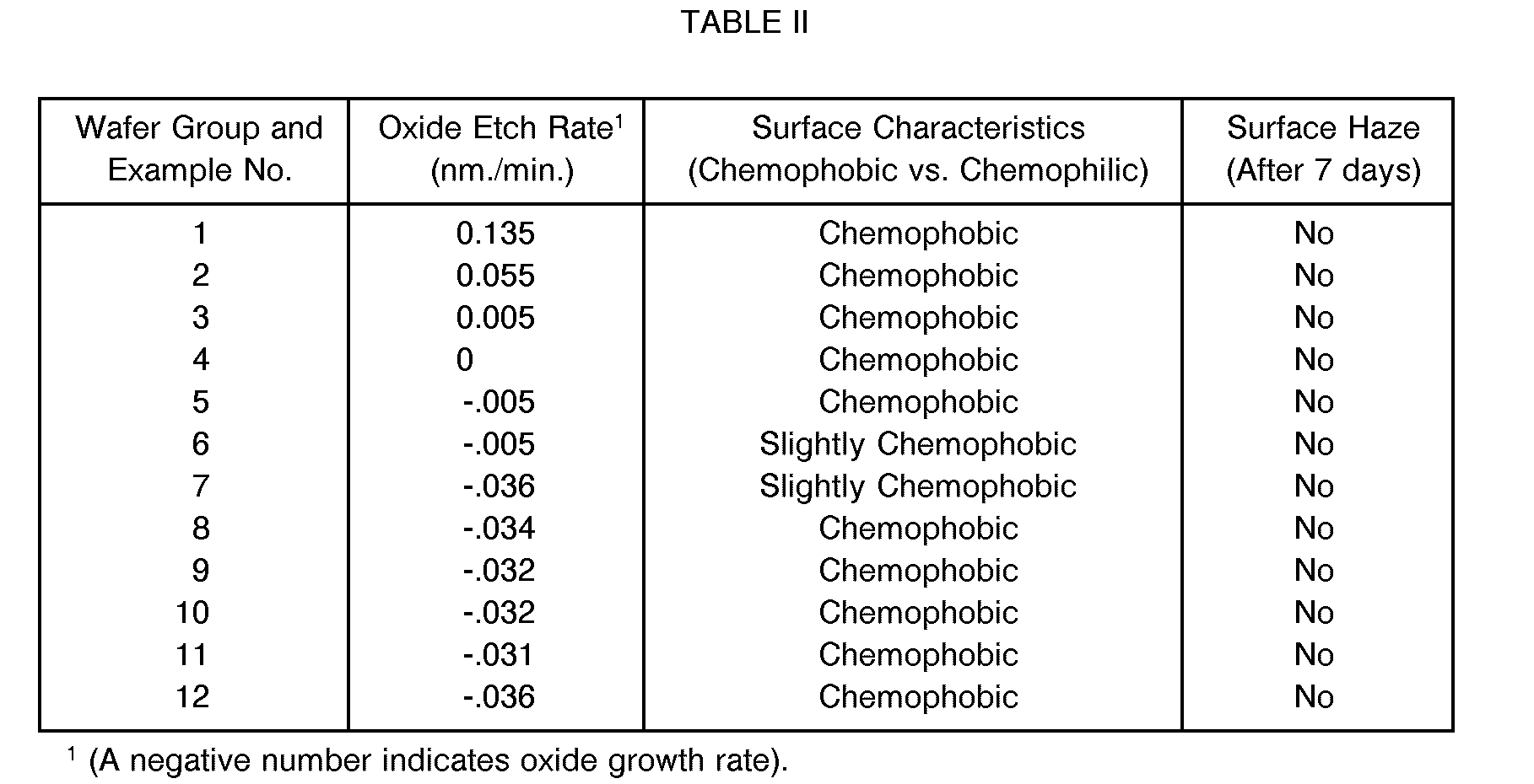
- Oxide coated silicon wafers (Examples 1-6) or bare silicon monitor wafers (Examples 7-12) were contacted with solutions, containing sulfuric acid, hydrogen peroxide and varying amounts of hydrofluoric acid, as outlined in TABLE I below.
- the procedure involved first immersing the wafers in the solutions at 100°C for 10 minutes. After that, the wafers were rinsed with deionized water at 45°C for 5 minutes. This was followed by another rinse, again with deionized water, but at a temperature of 22°C for 5 minutes. The wafers were then spun dry for 4 minutes in hot flowing air. In each case, it was found that the oxide etch rate was less than 0.2 nm/min., and a hydrophobic surface was established, with no noticeable surface haze after 7 days. The results of these tests are summarized in TABLE II below.
- Example 13 the procedure of Example 1 was followed, except that the wafers were bare silicon monitor wafers, and after the wafers were spun dry, a 400 nm thick layer of polysilicon was deposited by standard CVD techniques.
- the solution contained sulfuric acid, hydrogen peroxide and hydrofluoric acid, while in Comparative Examples A and B, the solutions contained sulfuric acid and hydrogen peroxide, but no hydrofluoric acid was added.
- the compositions of the solutions are outlined in TABLE III below.
- Example 14 the procedure of Example 1 was followed, except that the wafers were bare silicon monitor wafers, and after the wafers were spun dry, a 400 nm thick layer of polysilicon was deposited by standard CVD techniques.
- the solution contained sulfuric acid, hydrogen peroxide and hydrofluoric acid, while in Comparative Examples C and D, the solutions contained sulfuric acid and hydrogen peroxide, but no hydrofluoric acid was added.
- the compositions of the solutions are outlined in TABLE V below.
Abstract
A substantial reduction in the foreign particulate matter contamination on surfaces, such as the surfaces of semiconductor wafers, is achieved by treating the surfaces with a solution comprising a strong acid and a very small amount of a fluorine-containing compound. A preferred method employs a solution containing sulfuric acid, hydrogen peroxide and a very small amount of hydrofluoric acid, which is effective in reducing foreign particulate matter contamination, without significant etching, of the surface being treated.
Description
- This invention relates to the cleaning of surfaces, and, more particularly, to an improved method of reducing foreign particulate matter on surfaces of semiconductor wafers.
- In the manufacture of semiconductor devices, cleaning steps are performed before or after various steps to remove foreign contaminants or impurities from the surfaces of semiconductor wafers. For example, wafers are commonly polished with abrasive slurries to produce smooth, polished surfaces; after polishing, it is necessary to remove the slurry and other surface contaminants from the wafers. Removal of foreign particulate matter, such as metallics and organic contaminants, is also required prior to high temperature processing steps, such as diffusion, thermal oxidation and epitaxial growth; otherwise, these impurities can adversely affect surface stability, reliability, electrical performance and production yield of devices. Cleaning steps are also commonly carried out after stripping photoresist materials from the surfaces of wafers and following etching steps.
- Various techniques are used to clean foreign particulate matter from the surfaces of semiconductor wafers, such as chemical removal, centrifugation, air-stream or water jet cleaning, mechanical scrubbing and so forth. One commonly used chemical cleaning solution contains sulfuric acid and hydrogen peroxide (see, for example, Kern, W., "Hydrogen Peroxide Solutions For Silicon Wafer Cleaning", RCA Engineer, 28-4 (Jul./Aug. 1983), pp. 99-105), but that solution is somewhat limited in its foreign particulate matter removal effectiveness. Other methods employing various cleaning solutions are exemplified by the disclosures in the following: US-A-4 261 791, US-A-4 711 256 and US-A-4 828 751.
- Now, an improved method has been discovered for reducing foreign particulate matter on a surface, particularly a surface of a semiconductor wafer. In accordance with the invention, the surface to be treated is contacted with a solution comprising a strong acid and a very small amount of a fluorine-containing compound, which is effective in reducing foreign particulate matter contamination, without significant etching, of the surface. In a preferred method, there is employed a solution which further contains an oxidizing agent, such as hydrogen peroxide, and in which the fluorine-containing compound is hydrofluoric acid.
- In the practice of the invention, a substantial reduction, e.g. an order of magnitude or greater, in the foreign particulate matter concentration on the surface being treated has been achieved.
- It should be noted that various etching solutions are known which contain hydrofluoric acid, such as those disclosed in GB-A-989 025 and US-A-4 100 014. See also US-A-2 809 103; US-A-4 220 706, US-A-4 681 657 and US-A-4 705 760. Surprisingly, however, in view of these disclosures, it has now been found, that a substantial improvement in reducing foreign particulate matter concentration can be effected without significant etching of the surface being treated. The reduction occurs as a result of removing foreign particulate matter from the surface and repelling further contamination of the surface from the solution itself.
- As discussed above, the solution employed according to the invention, comprises a strong acid and a very small amount of a fluorine-containing compound. Any suitable strong acid can be employed, such as sulfuric acid, nitric acid and trifluoracetic acid, although sulfuric acid is preferred. A particularly preferred fluorine-containing compound is hydrofluoric acid.
- In carrying out the method, a very small amount of the fluorine-containing compound is employed. This amount is effective in reducing foreign particulate matter contamination of the surface being treated, but without significant etching of the surface. Without being bound by theory, it is believed that this is accomplished by establishing a chemophobic surface upon contacting the surface with the solution, in contrast with a chemophilic surface.
- Generally speaking, when a wafer surface is contacted with a conventional cleaning solution, a chemophilic surface is formed, with a residual film of the solution remaining on the surface. Foreign particulate matter from the solution is essentially trapped by the residual film on the surface being cleaned. These particulate contaminants once on the surface resist removal with cleaning solutions ordinarily employed by those skilled in the art. It is believed, however, that the method of the invention provides a chemophobic condition on the surface, where no observable residual film of the solution remains, although tiny droplets may still be present. With this condition, the solution and particulate contaminants are allowed to drain, thus producing a haze-free surface.
- It is important to note, however, that although the fluorine-containing compound is employed in an amount which is sufficient to establish a chemophobic surface, it does not cause etching of the surface to a significant extent. In general, the amount is such that the surface being treated is etched at a rate of less than about 2 nm/min., preferably less than about 0.5 nm/min., and most preferably less than about 0.2 nm/min.
- In general, the exact amount of the fluorine-containing compound that is employed will depend upon the nature of the compound, the temperature of the solution, the contacting time, etc. However, for hydrofluoric acid, the amount will usually range up to about 2.5 x 10⁻³ percent by weight, and more preferably up to about 2 x 10⁻⁴ percent by weight, based on the weight of the solution.
- Various other ingredients may be added to the solution. For example, a suitable oxidizing agent, such as hydrogen peroxide or nitric acid, may be added to further enhance the cleaning rate of the solution, with hydrogen peroxide being preferred. The amount of oxidizing agent employed may vary widely, but it typically ranges from about 5 to about 25 percent, based on the weight of the strong acid in the solution. Other ingredients may be added, depending on the nature of the surface being treated, as well as the nature of the particulate matter. For example, phosphoric acid may be added if particles of silicon nitride are being removed from the surface, as well as standard ingredients such as surfactants.
- In carrying out the method of the invention, the wafers are preferably immersed in the solution. Generally, this is performed at a temperature ranging from ambient to about 150°C, and preferably from about 90° to about 115°C, and for a period of time ranging from about a few seconds to about 10 minutes. The actual temperature and time will vary, however, depending on a number of factors, such as the exact formulation of the solution, the nature of the surface being treated and of the particulate matter being removed, and so forth, as will be apparent to those skilled in the art.
- Generally, the wafers are then rinsed, preferably with deionized water. Typically, this is performed in two steps, first with hot deionized water, such as at a temperature ranging from about 30° to about 90°C, preferably from about 40° to about 50°C, for about 1 to about 10 minutes, followed by a final rinse, at a temperature ranging from about 20°C to about 25°C for about 1 to about 10 minutes. Then, the wafers are usually subjected to a drying step, such as in a centrifuge.
- In addition, it should be noted that besides treating silicon-containing surfaces, such as silicon and silicon oxide, the method of the invention can be effectively used in treating a wide variety of surfaces of other substrates, such as oxides, metals, glasses, etc.
- The following examples are provided to illustrate the invention.
- Oxide coated silicon wafers (Examples 1-6) or bare silicon monitor wafers (Examples 7-12) were contacted with solutions, containing sulfuric acid, hydrogen peroxide and varying amounts of hydrofluoric acid, as outlined in TABLE I below. The procedure involved first immersing the wafers in the solutions at 100°C for 10 minutes. After that, the wafers were rinsed with deionized water at 45°C for 5 minutes. This was followed by another rinse, again with deionized water, but at a temperature of 22°C for 5 minutes. The wafers were then spun dry for 4 minutes in hot flowing air. In each case, it was found that the oxide etch rate was less than 0.2 nm/min., and a hydrophobic surface was established, with no noticeable surface haze after 7 days. The results of these tests are summarized in TABLE II below.

- In each of these examples, the procedure of Example 1 was followed, except that the wafers were bare silicon monitor wafers, and after the wafers were spun dry, a 400 nm thick layer of polysilicon was deposited by standard CVD techniques. In Example 13, the solution contained sulfuric acid, hydrogen peroxide and hydrofluoric acid, while in Comparative Examples A and B, the solutions contained sulfuric acid and hydrogen peroxide, but no hydrofluoric acid was added. The compositions of the solutions are outlined in TABLE III below.
- Particle counts were then determined, by employing a TENCOR Model 4000 or Model 5500 measurement tool (commercially available from Tencor Instruments, Mountain View, California). The resulting particle counts are summarized in TABLE IV below. It should be noted that the numerical result indicates the number of particles on the wafer having a size of 0.7 or 1.2 µ, respectively, or larger, measured in cross-sectional area. As shown in TABLE IV, the use of the solution of Example 13 showed a substantial reduction in foreign particulate matter concentration, as compared with the use of the standard H2 S04/H2 02 cleaning solution. In addition, the wafer treated with the solution in Example 13 did not show a noticeable haze after 90 days, while the wafers treated with the solutions in Comparative Examples A and B did show a noticeable haze after only 2 days.


- In each of these examples, the procedure of Example 1 was followed, except that the wafers were bare silicon monitor wafers, and after the wafers were spun dry, a 400 nm thick layer of polysilicon was deposited by standard CVD techniques. In Examples 14 and 15, the solution contained sulfuric acid, hydrogen peroxide and hydrofluoric acid, while in Comparative Examples C and D, the solutions contained sulfuric acid and hydrogen peroxide, but no hydrofluoric acid was added. The compositions of the solutions are outlined in TABLE V below.
- Particle counts were then determined, by employing a TENCOR Model 4000 or Model 5500 measurement tool (commercially available from Tencor Instruments, Mountain View, California). The resulting particle counts are summarized in TABLE VI below. It should be noted that the numerical result indicates the number of particles on the wafer having a size of 0.7 or 1.2 µ, respectively, or larger, measured in cross-sectional area. As shown in TABLE VI, the use of the solutions of Examples 14 and 15 showed a substantial reduction in foreign particulate matter concentration, as compared with the use of the standard H2 S04/H2 02 cleaning solution. In addition, the wafers treated with the solutions in Examples 14 and 15 did not show a noticeable haze after 90 days, while the wafers treated with the solutions in Comparative Examples C and D did show a noticeable haze after only 2 days.


Claims (10)
1. A method of treating a surface, which comprises contacting said surface with a solution comprising a strong acid and a very small amount of a fluorine-containing compound, which is effective in reducing foreign particulate matter contamination, without significant etching, of said surface.
2. The method of claim 1, wherein said amount of said fluorine-containing compound is sufficient to establish a chemophobic surface, without significant etching of said surface being treated.
3. The method of claim 1 or 2, wherein said fluorine-containing compound comprises hydrofluoric acid.
4. The method of any of the preceding claims 1 to 3, wherein said solution contains hydrofluoric acid in an amount of up to about 2.5 x 10⁻³ percent by weight and preferably in an amount of up to about 2 x 10⁻⁴ percent by weight.
5. The method of any of the preceding claims 1 to 4, wherein said strong acid is selected from the group consisting of sulfuric acid, nitric acid and trifluoroacetic acid.
6. The method of any of the preceding claims 1 to 5, wherein said surface is etched at a rate of less than about 0.5 nm/min and preferably at a rate of less than about 0.2 nm/min.
7. The method of any of the preceding claims 1 to 6, wherein said surface is contacted with said solution for a period of time ranging from about a few seconds to about 10 minutes, and wherein said solution is maintained at a temperature ranging from about 90° to about 115°C.
8. The method of any of the preceding claims 1 to 7, wherein said solution further comprises an oxidizing agent.
9. The method of claim 8, wherein said oxidizing agent comprises hydrogen peroxide.
10. The method of any of the preceding claims 1 to 9, wherein said surface is the surface of a semiconductor wafer.
Applications Claiming Priority (2)
| Application Number | Priority Date | Filing Date | Title |
|---|---|---|---|
| US58822890A | 1990-09-26 | 1990-09-26 | |
| US588228 | 1990-09-26 |
Publications (1)
| Publication Number | Publication Date |
|---|---|
| EP0477504A1 true EP0477504A1 (en) | 1992-04-01 |
Family
ID=24353005
Family Applications (1)
| Application Number | Title | Priority Date | Filing Date |
|---|---|---|---|
| EP91112984A Withdrawn EP0477504A1 (en) | 1990-09-26 | 1991-08-02 | Reduction of foreign particulate matter on semiconductor wafers |
Country Status (3)
| Country | Link |
|---|---|
| US (1) | US5294570A (en) |
| EP (1) | EP0477504A1 (en) |
| JP (1) | JP2787788B2 (en) |
Cited By (12)
| Publication number | Priority date | Publication date | Assignee | Title |
|---|---|---|---|---|
| EP0501492A2 (en) * | 1991-02-27 | 1992-09-02 | OKMETIC Oyj | Method for cleaning semiconductor products |
| EP0536747A2 (en) * | 1991-10-11 | 1993-04-14 | Air Products And Chemicals, Inc. | Halogenated carboxylic acid cleaning agents for fabricating integrated circuits and a process for using the same |
| EP0618612A2 (en) * | 1993-03-23 | 1994-10-05 | Matsushita Electric Industrial Co., Ltd. | Method of cleaning semiconductor device and equipment for cleaning semiconductor device |
| WO1994027314A1 (en) * | 1993-05-13 | 1994-11-24 | Interuniversitair Microelektronica Centrum | Method for semiconductor processing using mixtures of hf and carboxylic acid |
| EP0649168A2 (en) * | 1993-10-19 | 1995-04-19 | Nippon Steel Corporation | A cleaning solution and its use for cleaning silicon semiconductors and silicon oxides |
| EP0777265A3 (en) * | 1995-11-29 | 1998-12-23 | Kabushiki Kaisha Toshiba | Method and device for dissolving surface layer of semiconductor substrate |
| US5861064A (en) * | 1997-03-17 | 1999-01-19 | Fsi Int Inc | Process for enhanced photoresist removal in conjunction with various methods and chemistries |
| EP0918081A1 (en) * | 1997-11-21 | 1999-05-26 | International Business Machines Corporation | Etching composition and use |
| WO2004001834A1 (en) * | 2002-06-22 | 2003-12-31 | Merck Patent Gmbh | Composition for removing sidewall residues |
| WO2004076605A1 (en) * | 2003-02-25 | 2004-09-10 | Applied Materials, Inc. | Dilute sulfuric peroxide at point-of-use |
| DE19829863B4 (en) * | 1997-10-29 | 2006-06-29 | Mitsubishi Denki K.K. | Method for producing a semiconductor device |
| EP1884280A1 (en) * | 2006-08-03 | 2008-02-06 | Tokyo Electron Limited | Chemical-liquid mixing method and apparatus for the cleaning of substrates such as semiconductor wafers |
Families Citing this family (42)
| Publication number | Priority date | Publication date | Assignee | Title |
|---|---|---|---|---|
| JP3277404B2 (en) * | 1993-03-31 | 2002-04-22 | ソニー株式会社 | Substrate cleaning method and substrate cleaning apparatus |
| WO1995004372A1 (en) * | 1993-07-30 | 1995-02-09 | Semitool, Inc. | Methods for processing semiconductors to reduce surface particles |
| US5632866A (en) * | 1994-01-12 | 1997-05-27 | Fsi International, Inc. | Point-of-use recycling of wafer cleaning substances |
| JP2762230B2 (en) * | 1994-03-25 | 1998-06-04 | 信越半導体株式会社 | Storage method of silicon wafer |
| US5597443A (en) * | 1994-08-31 | 1997-01-28 | Texas Instruments Incorporated | Method and system for chemical mechanical polishing of semiconductor wafer |
| US5486266A (en) * | 1994-09-01 | 1996-01-23 | Taiwan Semiconductor Manuf. Company | Method for improving the adhesion of a deposited metal layer |
| EP1046433B1 (en) * | 1995-10-13 | 2004-01-02 | Lam Research Corporation | Method for removing contaminants by brushing |
| EP0797243A3 (en) * | 1996-03-07 | 1999-06-16 | Texas Instruments Incorporated | Etching process for dielectric layers in semiconductor devices |
| WO1997036209A1 (en) * | 1996-03-22 | 1997-10-02 | Merck Patent Gmbh | Solutions and processes for removal of sidewall residue after dry-etching________________________________________________________ |
| KR100528266B1 (en) * | 1996-03-22 | 2006-03-09 | 바스프 악티엔게젤샤프트 | Solution for removing residual wall residue after dry etching |
| US6273959B1 (en) | 1996-07-08 | 2001-08-14 | Matsushita Electric Industrial Co., Ltd. | Method of cleaning semiconductor device |
| US5817182A (en) * | 1997-03-07 | 1998-10-06 | Texas Instruments Incorporated | Hydrofluoric etch quenching via a colder rinse process |
| US20030209514A1 (en) * | 1997-04-04 | 2003-11-13 | Infineon Technologies North America Corp. | Etching composition and use thereof with feedback control of HF in BEOL clean |
| US6240933B1 (en) | 1997-05-09 | 2001-06-05 | Semitool, Inc. | Methods for cleaning semiconductor surfaces |
| US6482269B1 (en) * | 1997-05-29 | 2002-11-19 | Memc Electronic Materials, Inc. | Process for the removal of copper and other metallic impurities from silicon |
| US6200896B1 (en) | 1998-01-22 | 2001-03-13 | Cypress Semiconductor Corporation | Employing an acidic liquid and an abrasive surface to polish a semiconductor topography |
| US5858861A (en) * | 1998-05-15 | 1999-01-12 | Taiwan Semiconductor Manufacturing Company, Ltd. | Reducing nitride residue by changing the nitride film surface property |
| US6604086B1 (en) | 1998-07-20 | 2003-08-05 | Usa Technologies, Inc. | Electronic commerce terminal connected to a vending machine operable as a telephone |
| US6763336B1 (en) | 1998-07-20 | 2004-07-13 | Usa Technologies, Inc. | Method of transacting an electronic mail, an electronic commerce, and an electronic business transaction by an electronic commerce terminal using a wirelessly networked plurality of portable digital devices |
| US6609102B2 (en) | 1998-07-20 | 2003-08-19 | Usa Technologies, Inc. | Universal interactive advertizing and payment system for public access electronic commerce and business related products and services |
| US6615183B1 (en) | 1998-07-20 | 2003-09-02 | Usa Technologies, Inc. | Method of warehousing user data entered at an electronic commerce terminal |
| US6383723B1 (en) * | 1998-08-28 | 2002-05-07 | Micron Technology, Inc. | Method to clean substrate and improve photoresist profile |
| US5972124A (en) * | 1998-08-31 | 1999-10-26 | Advanced Micro Devices, Inc. | Method for cleaning a surface of a dielectric material |
| US6232231B1 (en) | 1998-08-31 | 2001-05-15 | Cypress Semiconductor Corporation | Planarized semiconductor interconnect topography and method for polishing a metal layer to form interconnect |
| US6162565A (en) | 1998-10-23 | 2000-12-19 | International Business Machines Corporation | Dilute acid rinse after develop for chrome etch |
| US6173720B1 (en) | 1998-12-02 | 2001-01-16 | International Business Machines Corporation | Process for treating a semiconductor substrate |
| US6248704B1 (en) | 1999-05-03 | 2001-06-19 | Ekc Technology, Inc. | Compositions for cleaning organic and plasma etched residues for semiconductors devices |
| US6794229B2 (en) | 2000-04-28 | 2004-09-21 | Semiconductor Energy Laboratory Co., Ltd. | Manufacturing method for semiconductor device |
| TW527443B (en) * | 2000-07-28 | 2003-04-11 | Infineon Technologies Corp | Etching composition and use thereof with feedback control of HF in BEOL clean |
| US6951221B2 (en) * | 2000-09-22 | 2005-10-04 | Dainippon Screen Mfg. Co., Ltd. | Substrate processing apparatus |
| US7805338B2 (en) * | 2001-03-26 | 2010-09-28 | Usa Technologies, Inc. | Method of constructing a digital content play list for transmission and presentation on a public access electronic terminal |
| US6969684B1 (en) | 2001-04-30 | 2005-11-29 | Cypress Semiconductor Corp. | Method of making a planarized semiconductor structure |
| US20030104680A1 (en) * | 2001-11-13 | 2003-06-05 | Memc Electronic Materials, Inc. | Process for the removal of copper from polished boron-doped silicon wafers |
| US6656852B2 (en) | 2001-12-06 | 2003-12-02 | Texas Instruments Incorporated | Method for the selective removal of high-k dielectrics |
| US6828678B1 (en) | 2002-03-29 | 2004-12-07 | Silicon Magnetic Systems | Semiconductor topography with a fill material arranged within a plurality of valleys associated with the surface roughness of the metal layer |
| US7718009B2 (en) | 2004-08-30 | 2010-05-18 | Applied Materials, Inc. | Cleaning submicron structures on a semiconductor wafer surface |
| JP2008270824A (en) * | 2008-05-09 | 2008-11-06 | Renesas Technology Corp | Method for manufacturing semiconductor device |
| US20100180939A1 (en) * | 2009-01-22 | 2010-07-22 | Sharma Pramod K | Heat treatable magnesium fluoride inclusive coatings, coated articles including heat treatable magnesium fluoride inclusive coatings, and methods of making the same |
| JP5066152B2 (en) * | 2009-09-25 | 2012-11-07 | 株式会社東芝 | Cleaning system |
| US20110274766A1 (en) | 2010-05-05 | 2011-11-10 | Allen Randall R | Synergy of Strong Acids and Peroxy Compounds |
| US8668777B2 (en) | 2010-12-22 | 2014-03-11 | Lam Research Ag | Process for treating a semiconductor wafer |
| JP6493839B2 (en) * | 2015-03-24 | 2019-04-03 | 株式会社Screenホールディングス | Substrate processing method and substrate processing apparatus |
Citations (2)
| Publication number | Priority date | Publication date | Assignee | Title |
|---|---|---|---|---|
| US4220706A (en) * | 1978-05-10 | 1980-09-02 | Rca Corporation | Etchant solution containing HF-HnO3 -H2 SO4 -H2 O2 |
| US4261791A (en) * | 1979-09-25 | 1981-04-14 | Rca Corporation | Two step method of cleaning silicon wafers |
Family Cites Families (13)
| Publication number | Priority date | Publication date | Assignee | Title |
|---|---|---|---|---|
| US2809103A (en) * | 1953-11-10 | 1957-10-08 | Sylvania Electric Prod | Fabrication of semiconductor elements |
| NL266733A (en) * | 1961-07-05 | |||
| JPS49107476A (en) * | 1973-02-15 | 1974-10-12 | ||
| DE2638302A1 (en) * | 1976-08-25 | 1978-03-02 | Wacker Chemitronic | DETERGENT FOR III / V SEMICONDUCTORS |
| US4711256A (en) * | 1985-04-19 | 1987-12-08 | Robert Kaiser | Method and apparatus for removal of small particles from a surface |
| US4681657A (en) * | 1985-10-31 | 1987-07-21 | International Business Machines Corporation | Preferential chemical etch for doped silicon |
| US4705760A (en) * | 1986-01-16 | 1987-11-10 | Rca Corporation | Preparation of a surface for deposition of a passinating layer |
| JPS63244624A (en) * | 1987-03-30 | 1988-10-12 | Nec Corp | Treatment of silicon substrate |
| US4828751A (en) * | 1987-08-28 | 1989-05-09 | Pcr, Inc. | Solvent composition for cleaning silicon wafers |
| JPH0752728B2 (en) * | 1987-09-18 | 1995-06-05 | 富士通株式会社 | Semiconductor cleaning method |
| JPH01265521A (en) * | 1988-04-15 | 1989-10-23 | Fujitsu Ltd | Cleaning of semiconductor substrate |
| US5181985A (en) * | 1988-06-01 | 1993-01-26 | Wacker-Chemitronic Gesellschaft Fur Elektronik-Grundstoffe Mbh | Process for the wet-chemical surface treatment of semiconductor wafers |
| JPH01316937A (en) * | 1988-06-15 | 1989-12-21 | Fujitsu Ltd | Cleaning of semiconductor substrate |
-
1991
- 1991-07-05 JP JP3164755A patent/JP2787788B2/en not_active Expired - Lifetime
- 1991-08-02 EP EP91112984A patent/EP0477504A1/en not_active Withdrawn
-
1992
- 1992-01-29 US US07/827,846 patent/US5294570A/en not_active Expired - Fee Related
Patent Citations (2)
| Publication number | Priority date | Publication date | Assignee | Title |
|---|---|---|---|---|
| US4220706A (en) * | 1978-05-10 | 1980-09-02 | Rca Corporation | Etchant solution containing HF-HnO3 -H2 SO4 -H2 O2 |
| US4261791A (en) * | 1979-09-25 | 1981-04-14 | Rca Corporation | Two step method of cleaning silicon wafers |
Non-Patent Citations (3)
| Title |
|---|
| International Electon Devices Meeting 1988, 11-14 December, San Francisco December 1988, pages 726 - 729; A. OHSAWA ET AL: "Improvements of trench capacitor characteristics by pre-oxidation surface cleaning with a HNO3-HF-H2O solution" * |
| JOURNAL OF THE ELECTROCHEMICAL SOCIETY. vol. 136, no. 1, January 1989, MANCHESTER, NEW HAMP pages 175 - 182; G. J. VALCO ET AL: "Plasma deposited silicon nitride for indium phosphide encapsulation" * |
| JOURNAL OF THE ELECTROCHEMICAL SOCIETY. vol. 136, no. 11, November 1989, MANCHESTER, NEW HAMP pages 3459 - 3462; T. SHIBATA ET AL: "Si surface cleaning and epitaxial growth of GaAs on Si by electron cyclotron resonance plasma-excited M-B-E at low temperatures" * |
Cited By (23)
| Publication number | Priority date | Publication date | Assignee | Title |
|---|---|---|---|---|
| EP0501492A2 (en) * | 1991-02-27 | 1992-09-02 | OKMETIC Oyj | Method for cleaning semiconductor products |
| EP0501492A3 (en) * | 1991-02-27 | 1993-03-10 | Okmetic Oy | Method for cleaning semiconductor products |
| EP0536747A2 (en) * | 1991-10-11 | 1993-04-14 | Air Products And Chemicals, Inc. | Halogenated carboxylic acid cleaning agents for fabricating integrated circuits and a process for using the same |
| EP0536747A3 (en) * | 1991-10-11 | 1993-05-26 | Air Products And Chemicals, Inc. | Halogenated carboxylic acid cleaning agents for fabricating integrated circuits and a process for using the same |
| EP0618612A2 (en) * | 1993-03-23 | 1994-10-05 | Matsushita Electric Industrial Co., Ltd. | Method of cleaning semiconductor device and equipment for cleaning semiconductor device |
| EP0618612A3 (en) * | 1993-03-23 | 1995-01-18 | Matsushita Electric Ind Co Ltd | Method of cleaning semiconductor device and equipment for cleaning semiconductor device. |
| WO1994027314A1 (en) * | 1993-05-13 | 1994-11-24 | Interuniversitair Microelektronica Centrum | Method for semiconductor processing using mixtures of hf and carboxylic acid |
| EP0649168A2 (en) * | 1993-10-19 | 1995-04-19 | Nippon Steel Corporation | A cleaning solution and its use for cleaning silicon semiconductors and silicon oxides |
| EP0649168A3 (en) * | 1993-10-19 | 1995-08-16 | Nippon Steel Corp | A cleaning solution and its use for cleaning silicon semiconductors and silicon oxides. |
| US5560857A (en) * | 1993-10-19 | 1996-10-01 | Nippon Steel Corporation | Solution for cleaning silicon semiconductors and silicon oxides |
| EP0777265A3 (en) * | 1995-11-29 | 1998-12-23 | Kabushiki Kaisha Toshiba | Method and device for dissolving surface layer of semiconductor substrate |
| US5861064A (en) * | 1997-03-17 | 1999-01-19 | Fsi Int Inc | Process for enhanced photoresist removal in conjunction with various methods and chemistries |
| DE19829863B4 (en) * | 1997-10-29 | 2006-06-29 | Mitsubishi Denki K.K. | Method for producing a semiconductor device |
| EP0918081A1 (en) * | 1997-11-21 | 1999-05-26 | International Business Machines Corporation | Etching composition and use |
| WO2004001834A1 (en) * | 2002-06-22 | 2003-12-31 | Merck Patent Gmbh | Composition for removing sidewall residues |
| CN100375250C (en) * | 2002-06-22 | 2008-03-12 | 巴斯福股份公司 | Composition for removing sidewall residues |
| US7417016B2 (en) | 2002-06-22 | 2008-08-26 | Basf Se | Composition for the removing of sidewall residues |
| US7531492B2 (en) | 2002-06-22 | 2009-05-12 | Basf Se | Composition for the removal of sidewall residues |
| WO2004076605A1 (en) * | 2003-02-25 | 2004-09-10 | Applied Materials, Inc. | Dilute sulfuric peroxide at point-of-use |
| EP1884280A1 (en) * | 2006-08-03 | 2008-02-06 | Tokyo Electron Limited | Chemical-liquid mixing method and apparatus for the cleaning of substrates such as semiconductor wafers |
| US9099502B2 (en) | 2006-08-03 | 2015-08-04 | Tokyo Electron Limited | Chemical-liquid mixing method and chemical-liquid mixing apparatus |
| US9339775B2 (en) | 2006-08-03 | 2016-05-17 | Tokyo Electron Limited | Chemical-liquid mixing method and chemical-liquid mixing apparatus |
| US9415356B1 (en) | 2006-08-03 | 2016-08-16 | Tokyo Electron Limited | Chemical-liquid mixing method and chemical-liquid mixing apparatus |
Also Published As
| Publication number | Publication date |
|---|---|
| JPH04234118A (en) | 1992-08-21 |
| JP2787788B2 (en) | 1998-08-20 |
| US5294570A (en) | 1994-03-15 |
Similar Documents
| Publication | Publication Date | Title |
|---|---|---|
| US5294570A (en) | Reduction of foreign particulate matter on semiconductor wafers | |
| US5679171A (en) | Method of cleaning substrate | |
| KR100220926B1 (en) | A cleaning method for hydrophobic silicon wafers | |
| JP3046208B2 (en) | Cleaning liquid for silicon wafer and silicon oxide | |
| WO1995004372A1 (en) | Methods for processing semiconductors to reduce surface particles | |
| US5782984A (en) | Method for cleaning an integrated circuit device using an aqueous cleaning composition | |
| JPH06295898A (en) | Selective removal of organometallic compound, residue of organosilicic compound and damaged/oxide | |
| EP0805484A1 (en) | Method of cleaning substrates | |
| WO2004076605B1 (en) | Dilute sulfuric peroxide at point-of-use | |
| EP0708480A1 (en) | Method of cleaning semiconductor wafers | |
| JP2841627B2 (en) | Semiconductor wafer cleaning method | |
| EP0926714A1 (en) | Silicon wafer storage water and silicon wafer storage method | |
| JP3528534B2 (en) | Cleaning method of silicon wafer | |
| JP3076202B2 (en) | Method of depositing polysilicon film for EG | |
| US6541391B2 (en) | Methods of cleaning surfaces of copper-containing materials, and methods of forming openings to copper-containing substrates | |
| US6955995B2 (en) | Methods of cleaning surfaces of copper-containing materials, and methods of forming openings to copper-containing substrates | |
| JPH0786220A (en) | Method of cleaning semiconductor wafer | |
| JPH10183185A (en) | Cleansing liquid, its formulation and production, cleansing, and production of semiconductor substrate | |
| EP0762488A2 (en) | Cleaning solution for cleaning semiconductor device and cleaning method using the same | |
| US20020175143A1 (en) | Processes for polishing wafers | |
| JPH0831781A (en) | Washing chemicals | |
| JP3040067B2 (en) | Method for cleaning substrate having semiconductor layer | |
| JPH06163496A (en) | Liquid for cleaning silicon wafer, and cleaning method | |
| US5972802A (en) | Prevention of edge stain in silicon wafers by ozone dipping | |
| JP2688293B2 (en) | Wafer surface cleaning method |
Legal Events
| Date | Code | Title | Description |
|---|---|---|---|
| PUAI | Public reference made under article 153(3) epc to a published international application that has entered the european phase |
Free format text: ORIGINAL CODE: 0009012 |
|
| AK | Designated contracting states |
Kind code of ref document: A1 Designated state(s): DE FR GB |
|
| STAA | Information on the status of an ep patent application or granted ep patent |
Free format text: STATUS: THE APPLICATION IS DEEMED TO BE WITHDRAWN |
|
| 18D | Application deemed to be withdrawn |
Effective date: 19921002 |