EP0477502B1 - Electronic circuit - Google Patents
Electronic circuit Download PDFInfo
- Publication number
- EP0477502B1 EP0477502B1 EP91112902A EP91112902A EP0477502B1 EP 0477502 B1 EP0477502 B1 EP 0477502B1 EP 91112902 A EP91112902 A EP 91112902A EP 91112902 A EP91112902 A EP 91112902A EP 0477502 B1 EP0477502 B1 EP 0477502B1
- Authority
- EP
- European Patent Office
- Prior art keywords
- electronic switch
- electrical
- control circuit
- bus bar
- circuit
- Prior art date
- Legal status (The legal status is an assumption and is not a legal conclusion. Google has not performed a legal analysis and makes no representation as to the accuracy of the status listed.)
- Expired - Lifetime
Links
Images

Classifications
-
- H—ELECTRICITY
- H01—ELECTRIC ELEMENTS
- H01M—PROCESSES OR MEANS, e.g. BATTERIES, FOR THE DIRECT CONVERSION OF CHEMICAL ENERGY INTO ELECTRICAL ENERGY
- H01M10/00—Secondary cells; Manufacture thereof
- H01M10/04—Construction or manufacture in general
- H01M10/0413—Large-sized flat cells or batteries for motive or stationary systems with plate-like electrodes
-
- H—ELECTRICITY
- H01—ELECTRIC ELEMENTS
- H01M—PROCESSES OR MEANS, e.g. BATTERIES, FOR THE DIRECT CONVERSION OF CHEMICAL ENERGY INTO ELECTRICAL ENERGY
- H01M10/00—Secondary cells; Manufacture thereof
- H01M10/06—Lead-acid accumulators
- H01M10/12—Construction or manufacture
- H01M10/122—Multimode batteries
-
- H—ELECTRICITY
- H01—ELECTRIC ELEMENTS
- H01M—PROCESSES OR MEANS, e.g. BATTERIES, FOR THE DIRECT CONVERSION OF CHEMICAL ENERGY INTO ELECTRICAL ENERGY
- H01M10/00—Secondary cells; Manufacture thereof
- H01M10/42—Methods or arrangements for servicing or maintenance of secondary cells or secondary half-cells
-
- H—ELECTRICITY
- H10—SEMICONDUCTOR DEVICES; ELECTRIC SOLID-STATE DEVICES NOT OTHERWISE PROVIDED FOR
- H10W—GENERIC PACKAGES, INTERCONNECTIONS, CONNECTORS OR OTHER CONSTRUCTIONAL DETAILS OF DEVICES COVERED BY CLASS H10
- H10W70/00—Package substrates; Interposers; Redistribution layers [RDL]
- H10W70/20—Conductive package substrates serving as an interconnection, e.g. metal plates
-
- H—ELECTRICITY
- H10—SEMICONDUCTOR DEVICES; ELECTRIC SOLID-STATE DEVICES NOT OTHERWISE PROVIDED FOR
- H10W—GENERIC PACKAGES, INTERCONNECTIONS, CONNECTORS OR OTHER CONSTRUCTIONAL DETAILS OF DEVICES COVERED BY CLASS H10
- H10W90/00—Package configurations
-
- H—ELECTRICITY
- H01—ELECTRIC ELEMENTS
- H01M—PROCESSES OR MEANS, e.g. BATTERIES, FOR THE DIRECT CONVERSION OF CHEMICAL ENERGY INTO ELECTRICAL ENERGY
- H01M10/00—Secondary cells; Manufacture thereof
- H01M10/04—Construction or manufacture in general
- H01M10/0445—Multimode batteries, e.g. containing auxiliary cells or electrodes switchable in parallel or series connections
-
- H—ELECTRICITY
- H10—SEMICONDUCTOR DEVICES; ELECTRIC SOLID-STATE DEVICES NOT OTHERWISE PROVIDED FOR
- H10W—GENERIC PACKAGES, INTERCONNECTIONS, CONNECTORS OR OTHER CONSTRUCTIONAL DETAILS OF DEVICES COVERED BY CLASS H10
- H10W72/00—Interconnections or connectors in packages
- H10W72/50—Bond wires
- H10W72/541—Dispositions of bond wires
- H10W72/5445—Dispositions of bond wires being orthogonal to a side surface of the chip, e.g. parallel arrangements
-
- H—ELECTRICITY
- H10—SEMICONDUCTOR DEVICES; ELECTRIC SOLID-STATE DEVICES NOT OTHERWISE PROVIDED FOR
- H10W—GENERIC PACKAGES, INTERCONNECTIONS, CONNECTORS OR OTHER CONSTRUCTIONAL DETAILS OF DEVICES COVERED BY CLASS H10
- H10W72/00—Interconnections or connectors in packages
- H10W72/50—Bond wires
- H10W72/541—Dispositions of bond wires
- H10W72/547—Dispositions of multiple bond wires
- H10W72/5473—Dispositions of multiple bond wires multiple bond wires connected to a common bond pad
-
- H—ELECTRICITY
- H10—SEMICONDUCTOR DEVICES; ELECTRIC SOLID-STATE DEVICES NOT OTHERWISE PROVIDED FOR
- H10W—GENERIC PACKAGES, INTERCONNECTIONS, CONNECTORS OR OTHER CONSTRUCTIONAL DETAILS OF DEVICES COVERED BY CLASS H10
- H10W72/00—Interconnections or connectors in packages
- H10W72/50—Bond wires
- H10W72/551—Materials of bond wires
- H10W72/552—Materials of bond wires comprising metals or metalloids, e.g. silver
- H10W72/5524—Materials of bond wires comprising metals or metalloids, e.g. silver comprising aluminium [Al]
-
- H—ELECTRICITY
- H10—SEMICONDUCTOR DEVICES; ELECTRIC SOLID-STATE DEVICES NOT OTHERWISE PROVIDED FOR
- H10W—GENERIC PACKAGES, INTERCONNECTIONS, CONNECTORS OR OTHER CONSTRUCTIONAL DETAILS OF DEVICES COVERED BY CLASS H10
- H10W72/00—Interconnections or connectors in packages
- H10W72/90—Bond pads, in general
- H10W72/931—Shapes of bond pads
- H10W72/932—Plan-view shape, i.e. in top view
-
- H—ELECTRICITY
- H10—SEMICONDUCTOR DEVICES; ELECTRIC SOLID-STATE DEVICES NOT OTHERWISE PROVIDED FOR
- H10W—GENERIC PACKAGES, INTERCONNECTIONS, CONNECTORS OR OTHER CONSTRUCTIONAL DETAILS OF DEVICES COVERED BY CLASS H10
- H10W90/00—Package configurations
- H10W90/701—Package configurations characterised by the relative positions of pads or connectors relative to package parts
- H10W90/751—Package configurations characterised by the relative positions of pads or connectors relative to package parts of bond wires
- H10W90/754—Package configurations characterised by the relative positions of pads or connectors relative to package parts of bond wires between a chip and a stacked insulating package substrate, interposer or RDL
-
- Y—GENERAL TAGGING OF NEW TECHNOLOGICAL DEVELOPMENTS; GENERAL TAGGING OF CROSS-SECTIONAL TECHNOLOGIES SPANNING OVER SEVERAL SECTIONS OF THE IPC; TECHNICAL SUBJECTS COVERED BY FORMER USPC CROSS-REFERENCE ART COLLECTIONS [XRACs] AND DIGESTS
- Y02—TECHNOLOGIES OR APPLICATIONS FOR MITIGATION OR ADAPTATION AGAINST CLIMATE CHANGE
- Y02E—REDUCTION OF GREENHOUSE GAS [GHG] EMISSIONS, RELATED TO ENERGY GENERATION, TRANSMISSION OR DISTRIBUTION
- Y02E60/00—Enabling technologies; Technologies with a potential or indirect contribution to GHG emissions mitigation
- Y02E60/10—Energy storage using batteries
-
- Y—GENERAL TAGGING OF NEW TECHNOLOGICAL DEVELOPMENTS; GENERAL TAGGING OF CROSS-SECTIONAL TECHNOLOGIES SPANNING OVER SEVERAL SECTIONS OF THE IPC; TECHNICAL SUBJECTS COVERED BY FORMER USPC CROSS-REFERENCE ART COLLECTIONS [XRACs] AND DIGESTS
- Y02—TECHNOLOGIES OR APPLICATIONS FOR MITIGATION OR ADAPTATION AGAINST CLIMATE CHANGE
- Y02P—CLIMATE CHANGE MITIGATION TECHNOLOGIES IN THE PRODUCTION OR PROCESSING OF GOODS
- Y02P70/00—Climate change mitigation technologies in the production process for final industrial or consumer products
- Y02P70/50—Manufacturing or production processes characterised by the final manufactured product
-
- Y—GENERAL TAGGING OF NEW TECHNOLOGICAL DEVELOPMENTS; GENERAL TAGGING OF CROSS-SECTIONAL TECHNOLOGIES SPANNING OVER SEVERAL SECTIONS OF THE IPC; TECHNICAL SUBJECTS COVERED BY FORMER USPC CROSS-REFERENCE ART COLLECTIONS [XRACs] AND DIGESTS
- Y10—TECHNICAL SUBJECTS COVERED BY FORMER USPC
- Y10T—TECHNICAL SUBJECTS COVERED BY FORMER US CLASSIFICATION
- Y10T29/00—Metal working
- Y10T29/49—Method of mechanical manufacture
- Y10T29/49002—Electrical device making
- Y10T29/49117—Conductor or circuit manufacturing
- Y10T29/49169—Assembling electrical component directly to terminal or elongated conductor
Definitions
- This invention relates to an electronic circuit device and particularly to an electronic power switching circuit which includes a heatsink.
- Power hybrid circuits commonly include silicon power switching devices, such as MOSFETs, mounted on electrically insulating ceramic members disposed on a metallic heatsink, such as copper.
- silicon power switching devices such as MOSFETs
- electrically insulating ceramic members disposed on a metallic heatsink, such as copper.
- the sandwich of silicon, ceramic and copper are joined into a sandwich by soldering, after which the electrical connections are made in any suitable manner, such as by wire bonding, which comprises ultrasonically welding aluminum wire to the silicon device and to a current-carrying electrode, for example.
- wire bonding which comprises ultrasonically welding aluminum wire to the silicon device and to a current-carrying electrode, for example.
- the joining of heat spreaders, ceramic insulators and silicon devices place the various electric terminals at different elevations, thereby requiring relatively long wire bonds which adversely affects performance and reliability.
- prior art heatsinks were fabricated by soldering or braising various sized blocks and plates to a base member to achieve uniform wire bond lengths,
- One application for power hybrid circuits of the type described is in a dual storage battery for automotive and similar uses.
- batteries include a primary cell unit which is used for normal operation and an auxiliary or reserve cell unit which is normally on standby. Should the primary unit become discharged, the auxiliary unit is switched into the vehicle's electrical circuity. This permits the vehicle to be started so that the primary unit can be recharged, after which the primary unit is switched into the circuit and the auxiliary unit returned to its reserve status.
- This application requires that the electronic switch devices carry momentarily high currents, such as, for example, in the order of several hundred amps or more. As a result, a substantial heatsink is required.
- a bus bar is directly connected with the control circuit and extends substantially vertical with respect to the main surface plane of said member. As the heights of the electronic switch and the control circuit are different to one another, relatively long wire bonds are required for the electrical conductor means connecting the electronic switch with the control circuit and the control circuit with the member.
- IBM T.D.B. 19(9), pages 3346 and 3347 discloses a power module with high power dissipation mounting a plurality of diodes or power transistors in a package in the form of an LSI circuit.
- This circuit is mounted on a metallized ceramic substrate by conventional techniques.
- the power transistors or diodes are connected to the circuit on the metallized by wire substrate bonds.
- the power transistors are back-bonded to a plate which acts as a heatsink. Said plate, in turn, can be mounted on a large heatsink.
- FIGURE 1 shows a lead acid storage battery 10 for any well-known purpose, such as, for example, automotive or marine use.
- Battery 10 has a first pair of terminals 11 and 12 mounted on the outer battery casing 13 and in circuit with the primary battery cells 14 (not shown) and a second pair of terminals 15 and 16 mounted within the casing 13 and in circuit with the auxiliary battery cells 17 (not shown).
- the primary battery cells 14 are normally in circuit with the apparatus being powered. Should the primary cells 14 become discharged, the auxiliary cells 17 are switched into the circuit for emergency power requirements.
- the electronic circuit devices for performing this switching operation and other control functions are mounted on a body 20 in accordance with the preferred embodiment of the invention which acts as a conductor and heatsink.
- the body 20 is suitably mounted in a suitable recess 21 formed in casing 13.
- the specific configuration of the member 20 will be dictated by its application, its electrical and thermal requirements, the configuration of the apparatus on which it is mounted, and the number, arrangement and type of electrical devices which it supports. Accordingly, the specific shape of the member 20 is only one example of the invention, it being understood that the invention encompasses other shapes as well.
- the heatsink and conductor 20 of the illustrated example is shown in FIGURES 2 and 3 to comprise a shaped body formed of a conductive material, such as copper.
- the body 20 is a unitary member formed in any suitable manner.
- the body 20 is formed by extruding an elongate copper member through an appropriately shaped die. The body 20 is then cut from the extruded member to a length which depends upon parameters such as current flow, ambient temperature, power dissipation, duty cycle and the like.
- the shape of the body 20 must be such as to accommodate the electrical devices being supported and cooled.
- heatsinks having different thermal requirements can be fabricated from a single extrusion. For example, merely by cutting the member to a greater or lesser length will control the amount of heat which can safely be dissipated.
- the intricately shaped members can be economically formed without mechanical or electrical transition joints.
- the member 20 has upper and lower surfaces 24 and 25, sides 26 and 27 and ends 29 and 30.
- a longitudinal channel 34 is formed in the upper surface 24 and intermediate the sides 26 and 27.
- the member 20 may be nickel-plated to facilitate soldering and wire bonding, thereby aiding in the manufacturing process.
- FIGURES 2 and 3 include various circuit components mounted on the member 20. It will be appreciated that the particular circuit components and their arrangement on member 20 are for purposes of illustration only, and that an infinite arrangement of such parts is possible. Also, as indicated above, the specific configuration of member 20 is dictated not only by its application, but also by the circuity which it supports. Therefore, it should be understood that the invention is not limited to the specifically illustrated embodiment, but only by the scope of the appended claims. With the foregoing in mind, the specific circuit configuration shown in the drawings will now be discussed.
- a plurality of power MOSFETs 42 are mounted on and are in direct thermal contact with the strip portion 38 of body 20.
- Control circuitry 44 for the MOSFETs 42 is formed on a substrate applied to a ceramic strip 46 mounted on the groove 24.
- the ceramic strip 46 provides support for and electrically insulates the control circuit 44 from the electrically conductive body 20.
- a bus bar 48 extends for substantially the length of the step 36 and is mounted on a second electrically insulating ceramic strip 50 supported by step 36.
- Wire bonds 56 connect the gate of each MOSFET 42 to a different one of the wire pads 57 which form a part of the control circuit 44.
- groups of wire bonds 59 couple the source of each MOSFET to an adjacent terminal 52. It is an important feature of the invention that the elevation and the location of the surfaces defined by the groove 24, the step 36 and the strip 38 are such that the terminations of the wire bonds are all at the same height and relatively close so that the wire bonds can be relatively short. Since the control circuit 44 and ceramic strip 46, the MOSFET 42 and the conductor 48 and ceramic strip 50 have different relative thicknesses, the surfaces defined by groove 24, strip 38 and step 36 are all at different relative heights on member 20 whereby the elevation of the respective terminals are at about the same elevation.
- each MOSFET 42 is in electrical contact with the body 20, which carries the relatively large currents being switched.
- each MOSFET 42 is in thermal contact with the body 20 for absorption and dissipation of heat generated during the switching and current-carrying operations.
- FIGURES 2 and 3 includes an integrated circuit 60 which provides MOSFET gate signals upon the receipt of command signals from an outside source (not shown) and a thermal sensor 62 coupled by wire bond 63 to the control circuit 44.
- wire bonds 64 and 65 may also be provided for connecting the control circuit 44 to the body 20 and to the terminal 67 mounted on bus bar 48.
- one of the battery terminals is connected to the bus bar 48 by conductor 68 and that the corresponding terminal of the auxiliary cells is connected by conductor 70 to terminal 72 on the body 20.
- the switching device is between the negative battery terminals 12 and 15, respectively, although switching could also be affected between the positive terminals 11 and 16, as well, in which event the negative terminals would be directly connected.
- the MOSFETs 42 are off and the negative auxiliary terminal 15 is disconnected from the negative battery terminal 12.
- the auxiliary cells 17 are disconnected from the vehicle's electrical system even though the positive primary battery terminal 11 is connected to the positive auxiliary battery terminal 16.
- terminal 15 is connected to terminal 12 thereby placing the auxiliary battery cells 17 in parallel with the primary battery cells 14.
- terminals 15 and 16 and the conductors 68 and 70 are located within the battery casing 13.
- FIGURE 5 shows a variation of the member 22' and includes a groove 24' for receiving the control circuit, a step 36' for receiving a bus bar and the strip 38' for receiving the MOSFETs.
- Other variations are also possible without deviating from the spirit of the invention.
- the method of manufacture according to the invention is not only less costly but also eliminates interfaces of relatively higher thermal and electrical resistance which reduce the effectiveness of the body as a conductor and heatsink.
- FIGURE 4 shows a further embodiment of the invention to include not only the switching circuit devices such as MOSFETs 142 for performing the battery switching operation discussed above, but also, there are a plurality of additional MOSFETs 143.
- the MOSFETs 142 are connected to the control circuit 144 and to the bus bar 148.
- the additional MOSFETs 143 are connected to the control circuit 144 and to terminal pads 149 which, in turn, are connected to other electrical devices being controlled.
- the terminal pads 149 may be connected to circuits controlling lighting, windshield wipers, door locks, window controls, etc.
- each of the terminal pads 149 are electrically isolated one from the other and from the member 120, while all of the switching circuit devices 142 are connected to bus bar 148.
- FIGURE 4 illustrates that merely by increasing the length of the heatsink and conductor member 120, additional circuit elements can be accommodated.
Landscapes
- Engineering & Computer Science (AREA)
- Manufacturing & Machinery (AREA)
- Chemical & Material Sciences (AREA)
- Chemical Kinetics & Catalysis (AREA)
- Electrochemistry (AREA)
- General Chemical & Material Sciences (AREA)
- Battery Mounting, Suspending (AREA)
- Fuses (AREA)
- Secondary Cells (AREA)
Description
- This invention relates to an electronic circuit device and particularly to an electronic power switching circuit which includes a heatsink.
- Power hybrid circuits commonly include silicon power switching devices, such as MOSFETs, mounted on electrically insulating ceramic members disposed on a metallic heatsink, such as copper. The sandwich of silicon, ceramic and copper are joined into a sandwich by soldering, after which the electrical connections are made in any suitable manner, such as by wire bonding, which comprises ultrasonically welding aluminum wire to the silicon device and to a current-carrying electrode, for example. The joining of heat spreaders, ceramic insulators and silicon devices place the various electric terminals at different elevations, thereby requiring relatively long wire bonds which adversely affects performance and reliability. To avoid these adverse effects, prior art heatsinks were fabricated by soldering or braising various sized blocks and plates to a base member to achieve uniform wire bond lengths, to vary the mass of the article and to support the required silicon devices.
- One application for power hybrid circuits of the type described is in a dual storage battery for automotive and similar uses. Such batteries include a primary cell unit which is used for normal operation and an auxiliary or reserve cell unit which is normally on standby. Should the primary unit become discharged, the auxiliary unit is switched into the vehicle's electrical circuity. This permits the vehicle to be started so that the primary unit can be recharged, after which the primary unit is switched into the circuit and the auxiliary unit returned to its reserve status. This application requires that the electronic switch devices carry momentarily high currents, such as, for example, in the order of several hundred amps or more. As a result, a substantial heatsink is required.
- In a prior art (US-A-4,314,270) electronic device comprising an elongate metallic member composed of a thermally and electrically conductive material, the electronic switch is mounted directly or via a copper plate on said member in electrical and thermal contact therewith. Electrical conductor means connect said electronic switch with the semiconductor control circuit in order to electrically connect the collector and gate electrodes of the electronic switch with the control circuit. The control circuit is electrically connected via a further electrical conductor means with said member in order to ground a potential point of the control circuit.
- A bus bar is directly connected with the control circuit and extends substantially vertical with respect to the main surface plane of said member. As the heights of the electronic switch and the control circuit are different to one another, relatively long wire bonds are required for the electrical conductor means connecting the electronic switch with the control circuit and the control circuit with the member.
- IBM T.D.B. 19(9), pages 3346 and 3347, discloses a power module with high power dissipation mounting a plurality of diodes or power transistors in a package in the form of an LSI circuit. This circuit is mounted on a metallized ceramic substrate by conventional techniques. The power transistors or diodes are connected to the circuit on the metallized by wire substrate bonds. The power transistors are back-bonded to a plate which acts as a heatsink. Said plate, in turn, can be mounted on a large heatsink.
- It is the object of the invention to provide a device and a method of manufacturing same in which adjustment of the thermal mass, the arrangement and mounting of silicon devices and thermal and electrical isolation is facilitated.
- This object is solved by the features as claimed in claims 1 and 5.
-
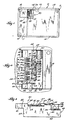
- FIGURE 1 is a top plan view of an automotive battery with which the electronic circuit device according to the invention may be employed;
- FIGURE 2 is a top plan view of the electronic circuit device according to the preferred embodiment of the invention;
- FIGURE 3 is a side elevational view of the electronic circuit device shown in FIGURE 2;
- FIGURE 4 is a top view of an alternate embodiment of the invention, and
- FIGURE 5 is a perspective view of an alternate embodiment of the invention.
- FIGURE 1 shows a lead acid storage battery 10 for any well-known purpose, such as, for example, automotive or marine use. Battery 10 has a first pair of
terminals 11 and 12 mounted on theouter battery casing 13 and in circuit with the primary battery cells 14 (not shown) and a second pair of terminals 15 and 16 mounted within thecasing 13 and in circuit with the auxiliary battery cells 17 (not shown). - As those skilled in the art will appreciate, the
primary battery cells 14 are normally in circuit with the apparatus being powered. Should theprimary cells 14 become discharged, the auxiliary cells 17 are switched into the circuit for emergency power requirements. The electronic circuit devices for performing this switching operation and other control functions are mounted on abody 20 in accordance with the preferred embodiment of the invention which acts as a conductor and heatsink. Thebody 20 is suitably mounted in a suitable recess 21 formed incasing 13. - It will be appreciated by those skilled in the art that the specific configuration of the
member 20 will be dictated by its application, its electrical and thermal requirements, the configuration of the apparatus on which it is mounted, and the number, arrangement and type of electrical devices which it supports. Accordingly, the specific shape of themember 20 is only one example of the invention, it being understood that the invention encompasses other shapes as well. - The heatsink and
conductor 20 of the illustrated example is shown in FIGURES 2 and 3 to comprise a shaped body formed of a conductive material, such as copper. Preferably, thebody 20 is a unitary member formed in any suitable manner. In the preferred embodiment of the invention, thebody 20 is formed by extruding an elongate copper member through an appropriately shaped die. Thebody 20 is then cut from the extruded member to a length which depends upon parameters such as current flow, ambient temperature, power dissipation, duty cycle and the like. In addition, the shape of thebody 20 must be such as to accommodate the electrical devices being supported and cooled. It can be seen that by fabricatingbody 20 by an extrusion process, heatsinks having different thermal requirements can be fabricated from a single extrusion. For example, merely by cutting the member to a greater or lesser length will control the amount of heat which can safely be dissipated. In addition, by employing extrusions, the intricately shaped members can be economically formed without mechanical or electrical transition joints. In addition, it is possible to form longitudinal grooves 23 in the surface ofmember 22 which facilitates soldering. - In the illustrated example, the
member 20 has upper andlower surfaces sides 26 and 27 and ends 29 and 30. Alongitudinal channel 34 is formed in theupper surface 24 and intermediate thesides 26 and 27. At theside 26, there is an area of reduced thickness which defines astep 36 which is below the level of thechannel 34. Between thestep 36 and thechannel 34 there is anelongate strip 38. At the opposite side 27 of themember 22, there is arecess 40 formed in the lower surface to facilitate mounting on the electrical device with which themember 20 is to be used, and which in the illustrated example, is the lead acid storage battery 10. Themember 20 may be nickel-plated to facilitate soldering and wire bonding, thereby aiding in the manufacturing process. - The illustrated embodiment shown in FIGURES 2 and 3 include various circuit components mounted on the
member 20. It will be appreciated that the particular circuit components and their arrangement onmember 20 are for purposes of illustration only, and that an infinite arrangement of such parts is possible. Also, as indicated above, the specific configuration ofmember 20 is dictated not only by its application, but also by the circuity which it supports. Therefore, it should be understood that the invention is not limited to the specifically illustrated embodiment, but only by the scope of the appended claims. With the foregoing in mind, the specific circuit configuration shown in the drawings will now be discussed. - In the example illustrated in FIGURES 2 and 3, a plurality of
power MOSFETs 42 are mounted on and are in direct thermal contact with thestrip portion 38 ofbody 20.Control circuitry 44 for theMOSFETs 42 is formed on a substrate applied to aceramic strip 46 mounted on thegroove 24. Theceramic strip 46 provides support for and electrically insulates thecontrol circuit 44 from the electricallyconductive body 20. Abus bar 48 extends for substantially the length of thestep 36 and is mounted on a second electrically insulating ceramic strip 50 supported bystep 36. In addition, there is aterminal 52 mounted on thebus bar 48 and opposite eachMOSFET 42 and afurther terminal 67 is formed on the bus bar and is adapted to be coupled to thecontrol circuit 44. -
Wire bonds 56 connect the gate of eachMOSFET 42 to a different one of the wire pads 57 which form a part of thecontrol circuit 44. In addition, groups of wire bonds 59 couple the source of each MOSFET to anadjacent terminal 52. It is an important feature of the invention that the elevation and the location of the surfaces defined by thegroove 24, thestep 36 and thestrip 38 are such that the terminations of the wire bonds are all at the same height and relatively close so that the wire bonds can be relatively short. Since thecontrol circuit 44 andceramic strip 46, theMOSFET 42 and theconductor 48 and ceramic strip 50 have different relative thicknesses, the surfaces defined bygroove 24,strip 38 and step 36 are all at different relative heights onmember 20 whereby the elevation of the respective terminals are at about the same elevation. - The drain of each
MOSFET 42 is in electrical contact with thebody 20, which carries the relatively large currents being switched. In addition, eachMOSFET 42 is in thermal contact with thebody 20 for absorption and dissipation of heat generated during the switching and current-carrying operations. - Other circuit components shown in FIGURES 2 and 3 includes an
integrated circuit 60 which provides MOSFET gate signals upon the receipt of command signals from an outside source (not shown) and athermal sensor 62 coupled by wire bond 63 to thecontrol circuit 44. Inaddition wire bonds 64 and 65 may also be provided for connecting thecontrol circuit 44 to thebody 20 and to the terminal 67 mounted onbus bar 48. - Referring again to FIGURE 1, it can be seen that one of the battery terminals is connected to the
bus bar 48 byconductor 68 and that the corresponding terminal of the auxiliary cells is connected by conductor 70 to terminal 72 on thebody 20. In the illustrated embodiment, the switching device is between thenegative battery terminals 12 and 15, respectively, although switching could also be affected between the positive terminals 11 and 16, as well, in which event the negative terminals would be directly connected. When the battery 10 is in normal operation, theMOSFETs 42 are off and the negative auxiliary terminal 15 is disconnected from thenegative battery terminal 12. As a result, the auxiliary cells 17 are disconnected from the vehicle's electrical system even though the positive primary battery terminal 11 is connected to the positive auxiliary battery terminal 16. When theMOSFETs 42 receive a gate signal and thereby become conductive, terminal 15 is connected to terminal 12 thereby placing the auxiliary battery cells 17 in parallel with theprimary battery cells 14. Those skilled in the art will appreciate that the terminals 15 and 16 and theconductors 68 and 70 are located within thebattery casing 13. - FIGURE 5 shows a variation of the member 22' and includes a groove 24' for receiving the control circuit, a step 36' for receiving a bus bar and the strip 38' for receiving the MOSFETs. Other variations are also possible without deviating from the spirit of the invention.
- It can be seen that because the
member 20 is formed from an extrusion and not from individual components which are joined by braising or soldering, the method of manufacture according to the invention is not only less costly but also eliminates interfaces of relatively higher thermal and electrical resistance which reduce the effectiveness of the body as a conductor and heatsink. - FIGURE 4 shows a further embodiment of the invention to include not only the switching circuit devices such as
MOSFETs 142 for performing the battery switching operation discussed above, but also, there are a plurality ofadditional MOSFETs 143. TheMOSFETs 142 are connected to thecontrol circuit 144 and to thebus bar 148. Theadditional MOSFETs 143 are connected to thecontrol circuit 144 and toterminal pads 149 which, in turn, are connected to other electrical devices being controlled. For example, if the invention is employed in an automotive application, theterminal pads 149 may be connected to circuits controlling lighting, windshield wipers, door locks, window controls, etc. In this example, each of theterminal pads 149 are electrically isolated one from the other and from themember 120, while all of theswitching circuit devices 142 are connected tobus bar 148. FIGURE 4 illustrates that merely by increasing the length of the heatsink andconductor member 120, additional circuit elements can be accommodated.
Claims (5)
- Electronic circuit device comprising an elongate metallic member (20,22,120) composed of a thermally and electrically conductive material, said member comprises a unitary mass defining a heatsink and being free of mechanical or electrical transition joints and includes first, second and third support surfaces, each located at a different relative elevation,at least one electronic switch (42, 142) mounted on said second support surface of said member (20,22',120) and in electrical and thermal contact therewith, a control circuit (44,144) mounted on said first support surface and a bus bar (48,148) mounted on said third support surface of said member and adjacent said electronic switch,a thermal and electrical barrier means (50) between said bus bar and said third support surface,a first electrical conductor means (56) connecting said control circuit to said electronic switch, said first electrical conductor means having terminals on opposite ends thereof,second electrical conductor means (59) connecting said electronic switch to said bus bar, said second electrical conductor means having terminals on opposite ends thereof,said member (20,22',120) acting as a heatsink for said electronic switch (42,142) and as a conductor for the current being switched thereby, whereinthe thickness of said control circuit (44,144), said electronic switch (42,142) and said bus bar (48,148) and the relative elevations of said first, second and third support surfaces being such that the terminals of said conductor means (56,59) are at the same elevation.
- Device set forth in claim 1 wherein there are a plurality of electronic switches (42,142) mounted on said second support surface, a first plurality of electrical conductor means (56) connecting said control circuit (44,144) to respective ones of said electronic switches (42,142) and a second plurality of electrical conductor means (59) connecting respective ones of said electronic switches to said bus bar (48,148) in a parallel circuit relation.
- Device set forth in claim 1 or 2 wherein there is a second electrical and heat barrier means (46) between said first support surface of said member (20,22',120) and said control circuit (44,144).
- Device set forth in one of the foregoing claims combined with a storage battery (10) having primary cells (14) and auxiliary cells (17),first and second terminal means (11,12) in circuit with the primary cells, and third and fourth terminal means (15,16) in circuit with the auxiliary cells, whereinsaid at least one electronic switch (42,142) is in circuit between said second and third terminal means (12,15) and operative to place said primary and auxiliary cells in a parallel circuit relation.
- A method of manufacturing an electronic circuit device comprising the steps of:extruding an elongate shaped member (20,22',120) formed of a metallic material having high thermal and electrical conductivity,severing a first predetermined length of said extruded member to provide a unitary member which defines a conductor and heatsink, is free of mechanical and electrical transition joints, and includes first,second and third support surfaces, each located at a different relative elevation;mounting at least one electronic switch (42,142) in thermal and electrical contact on said second support surface of said member,mounting a control circuit (44,144) on said first support surface and a bus bar (48,148) on said third support surface and adjacent said electronic switch (42,142), and electrically interconnecting said electronic switch with said control circuit and electrically interconnecting said electronic switch with said bus bar by first and second conductor means (56,59) said first and second conductor means each having terminals on opposite ends thereof, and electrically insulating said control circuit and said bus bar from said member, whereinthe thickness of said control circuit (44,144), said electronic switch (42,142) and said bus bar (48,148) and the relative elevations of said first, second and third support surfaces being such that the terminals of said conductor means (56,59) are at the same elevation.
Applications Claiming Priority (2)
| Application Number | Priority Date | Filing Date | Title |
|---|---|---|---|
| US574296 | 1990-08-28 | ||
| US07/574,296 US5153449A (en) | 1990-08-28 | 1990-08-28 | Heatsink bus for electronic switch |
Publications (2)
| Publication Number | Publication Date |
|---|---|
| EP0477502A1 EP0477502A1 (en) | 1992-04-01 |
| EP0477502B1 true EP0477502B1 (en) | 1997-03-05 |
Family
ID=24295507
Family Applications (1)
| Application Number | Title | Priority Date | Filing Date |
|---|---|---|---|
| EP91112902A Expired - Lifetime EP0477502B1 (en) | 1990-08-28 | 1991-07-31 | Electronic circuit |
Country Status (4)
| Country | Link |
|---|---|
| US (1) | US5153449A (en) |
| EP (1) | EP0477502B1 (en) |
| CA (1) | CA2047767A1 (en) |
| DE (1) | DE69124896T2 (en) |
Families Citing this family (22)
| Publication number | Priority date | Publication date | Assignee | Title |
|---|---|---|---|---|
| US5549984A (en) * | 1994-07-25 | 1996-08-27 | Globe-Union Inc. | Control and indicator circuit for a dual battery system |
| US5581443A (en) * | 1994-09-14 | 1996-12-03 | Kabushiki Kaisha Toshiba | Structure for cooling a circuit module having a circuit board and a heat-generating IC chip mounted on the board, and portable electronic apparatus incorporating the structure |
| US5784256A (en) * | 1994-09-14 | 1998-07-21 | Kabushiki Kaisha Toshiba | Portable computer having a circuit board including a heat-generating IC chip and a metal frame supporting the circuit board |
| US6295201B1 (en) * | 1998-08-04 | 2001-09-25 | Stratos Lightwave, Inc. | Bus bar having embedded switching device |
| US6508595B1 (en) * | 2000-05-11 | 2003-01-21 | International Business Machines Corporation | Assembly of opto-electronic module with improved heat sink |
| JP2001327044A (en) * | 2000-05-16 | 2001-11-22 | Auto Network Gijutsu Kenkyusho:Kk | Power distributor for vehicles |
| US6587346B1 (en) | 2002-01-31 | 2003-07-01 | Visteon Global Technologies, Inc. | Combination electrical power distribution and heat dissipating device |
| US7589500B2 (en) | 2002-11-22 | 2009-09-15 | Milwaukee Electric Tool Corporation | Method and system for battery protection |
| US7157882B2 (en) * | 2002-11-22 | 2007-01-02 | Milwaukee Electric Tool Corporation | Method and system for battery protection employing a selectively-actuated switch |
| US8471532B2 (en) | 2002-11-22 | 2013-06-25 | Milwaukee Electric Tool Corporation | Battery pack |
| US7270910B2 (en) * | 2003-10-03 | 2007-09-18 | Black & Decker Inc. | Thermal management systems for battery packs |
| US8068346B2 (en) * | 2004-05-04 | 2011-11-29 | Hamilton Sundstrand Corporation | Circuit board with high density power semiconductors |
| KR100936262B1 (en) * | 2005-10-21 | 2010-01-12 | 주식회사 엘지화학 | A bus bar for electrical connection with a novel structure and a battery module including the same |
| DE102007014120A1 (en) * | 2007-03-23 | 2008-09-25 | Ferm Bv | Power Pack |
| DE102007062167A1 (en) * | 2007-12-21 | 2009-06-25 | Robert Bosch Gmbh | power circuit |
| DE102008010837A1 (en) * | 2008-02-23 | 2009-08-27 | Daimler Ag | Battery with a arranged in a battery housing heat conducting plate for tempering the battery |
| US7812589B2 (en) * | 2008-08-28 | 2010-10-12 | Qualitau, Inc. | Modified current source (MCS) with seamless range switching |
| DE102009029476B4 (en) * | 2009-09-15 | 2012-11-08 | Lisa Dräxlmaier GmbH | Electronic device for switching currents and manufacturing method for the same |
| DE102013204675A1 (en) * | 2013-03-18 | 2014-10-02 | Robert Bosch Gmbh | Battery cell for a battery and method for producing a battery cell |
| USD745383S1 (en) * | 2014-09-16 | 2015-12-15 | Kelly Peters | Door lock stop device |
| US10052713B2 (en) * | 2015-08-20 | 2018-08-21 | Ultex Corporation | Bonding method and bonded structure |
| FR3060845B1 (en) * | 2016-12-19 | 2019-05-24 | Institut Vedecom | ELECTRONIC POWER CIRCUITS EQUIPPED WITH BAR BUSES FORMING THERMAL DISSIPATORS AND INTEGRATION METHOD |
Family Cites Families (13)
| Publication number | Priority date | Publication date | Assignee | Title |
|---|---|---|---|---|
| US3029301A (en) * | 1959-08-18 | 1962-04-10 | Pierce W Strider | Combination of 6 volt and 12 volt battery |
| DE2530157A1 (en) * | 1975-07-05 | 1977-02-03 | Bosch Gmbh Robert | ELECTRONIC CONTROL UNIT |
| US4314270A (en) * | 1977-12-02 | 1982-02-02 | Mitsubishi Denki Kabushiki Kaisha | Hybrid thick film integrated circuit heat dissipating and grounding assembly |
| US4360766A (en) * | 1978-09-19 | 1982-11-23 | Bogardus Jr Carl R | Multi-battery power supply for DC motors |
| DE2903102A1 (en) * | 1979-01-27 | 1980-07-31 | Dahlberg Reinhard | Electronic component with point contact structure - comprising two discs or plates of metal, ferromagnetic, superconductive or semiconductor material |
| EP0064856B1 (en) * | 1981-05-12 | 1986-12-30 | LUCAS INDUSTRIES public limited company | A multi-phase bridge arrangement |
| US4700273A (en) * | 1986-06-03 | 1987-10-13 | Kaufman Lance R | Circuit assembly with semiconductor expansion matched thermal path |
| FR2620296B1 (en) * | 1987-09-03 | 1990-01-19 | Bendix Electronics Sa | ELECTRONIC CIRCUIT BOX |
| US4905123A (en) * | 1987-10-08 | 1990-02-27 | Navistar International Transportation Corp. | Heat sink bus assembly |
| JPH064595Y2 (en) * | 1988-02-24 | 1994-02-02 | 日本電気株式会社 | Hybrid IC |
| US5039335A (en) * | 1988-10-21 | 1991-08-13 | Texas Instruments Incorporated | Composite material for a circuit system and method of making |
| US4901201A (en) * | 1988-10-25 | 1990-02-13 | Sundstrand Corporation | Plate fin/chic heat exchanger |
| BR9007436A (en) * | 1989-06-12 | 1992-04-28 | Globe Union Inc | DOUBLE SWITCHED BATTERY SYSTEM |
-
1990
- 1990-08-28 US US07/574,296 patent/US5153449A/en not_active Expired - Fee Related
-
1991
- 1991-07-24 CA CA002047767A patent/CA2047767A1/en not_active Abandoned
- 1991-07-31 EP EP91112902A patent/EP0477502B1/en not_active Expired - Lifetime
- 1991-07-31 DE DE69124896T patent/DE69124896T2/en not_active Expired - Fee Related
Also Published As
| Publication number | Publication date |
|---|---|
| US5153449A (en) | 1992-10-06 |
| EP0477502A1 (en) | 1992-04-01 |
| DE69124896D1 (en) | 1997-04-10 |
| CA2047767A1 (en) | 1992-03-01 |
| DE69124896T2 (en) | 1997-06-12 |
Similar Documents
| Publication | Publication Date | Title |
|---|---|---|
| US5153449A (en) | Heatsink bus for electronic switch | |
| US7545033B2 (en) | Low cost power semiconductor module without substrate | |
| EP0927433B1 (en) | Semiconductor device assemblies and circuits | |
| EP0962975B1 (en) | Power MOSFET package with directly connected leads | |
| US7149088B2 (en) | Half-bridge power module with insert molded heatsinks | |
| US9306020B2 (en) | Power module and method of manufacturing the power module | |
| US8188601B2 (en) | Semiconductor subassemblies with interconnects and methods for manufacturing the same | |
| US6479327B2 (en) | Semiconductor device and method for manufacturing the same | |
| JP2896126B2 (en) | Semiconductor devices and surface mount packages | |
| US6166464A (en) | Power module | |
| US9035453B2 (en) | Semiconductor device | |
| US7859079B2 (en) | Power semiconductor device | |
| US20080029906A1 (en) | Semiconductor switching module and method | |
| US20010045777A1 (en) | Power distributor for vehicle | |
| JP2006086438A (en) | Semiconductor module bus bar structure | |
| EP0418891B1 (en) | Moulded plastic power semiconductor device | |
| CN118137782A (en) | Power module for converter with improved signal pin field shielding | |
| US6281579B1 (en) | Insert-molded leadframe to optimize interface between powertrain and driver board | |
| US20220399259A1 (en) | Power Semiconductor Module | |
| US5324890A (en) | Direct bond copper-output footprint | |
| US20240194576A1 (en) | Power module for a vehicle | |
| CN218996706U (en) | Copper strip bonding type power module packaging structure for epoxy plastic package vehicle | |
| JP2002314037A (en) | Power semiconductor module | |
| CN222507615U (en) | Power chip packaging structure and printed circuit board assembly | |
| GB2642972A (en) | A power module |
Legal Events
| Date | Code | Title | Description |
|---|---|---|---|
| PUAI | Public reference made under article 153(3) epc to a published international application that has entered the european phase |
Free format text: ORIGINAL CODE: 0009012 |
|
| AK | Designated contracting states |
Kind code of ref document: A1 Designated state(s): CH DE FR GB IT LI SE |
|
| 17P | Request for examination filed |
Effective date: 19920827 |
|
| 17Q | First examination report despatched |
Effective date: 19941123 |
|
| GRAG | Despatch of communication of intention to grant |
Free format text: ORIGINAL CODE: EPIDOS AGRA |
|
| GRAH | Despatch of communication of intention to grant a patent |
Free format text: ORIGINAL CODE: EPIDOS IGRA |
|
| GRAH | Despatch of communication of intention to grant a patent |
Free format text: ORIGINAL CODE: EPIDOS IGRA |
|
| GRAA | (expected) grant |
Free format text: ORIGINAL CODE: 0009210 |
|
| ITF | It: translation for a ep patent filed | ||
| AK | Designated contracting states |
Kind code of ref document: B1 Designated state(s): CH DE FR GB IT LI SE |
|
| REG | Reference to a national code |
Ref country code: CH Ref legal event code: NV Representative=s name: PATENTANWALTSBUERO JEAN HUNZIKER Ref country code: CH Ref legal event code: EP |
|
| REF | Corresponds to: |
Ref document number: 69124896 Country of ref document: DE Date of ref document: 19970410 |
|
| ET | Fr: translation filed | ||
| PGFP | Annual fee paid to national office [announced via postgrant information from national office to epo] |
Ref country code: GB Payment date: 19970710 Year of fee payment: 7 |
|
| PGFP | Annual fee paid to national office [announced via postgrant information from national office to epo] |
Ref country code: FR Payment date: 19970716 Year of fee payment: 7 |
|
| PGFP | Annual fee paid to national office [announced via postgrant information from national office to epo] |
Ref country code: SE Payment date: 19970723 Year of fee payment: 7 |
|
| PGFP | Annual fee paid to national office [announced via postgrant information from national office to epo] |
Ref country code: CH Payment date: 19970820 Year of fee payment: 7 |
|
| PGFP | Annual fee paid to national office [announced via postgrant information from national office to epo] |
Ref country code: DE Payment date: 19970829 Year of fee payment: 7 |
|
| PLBE | No opposition filed within time limit |
Free format text: ORIGINAL CODE: 0009261 |
|
| STAA | Information on the status of an ep patent application or granted ep patent |
Free format text: STATUS: NO OPPOSITION FILED WITHIN TIME LIMIT |
|
| 26N | No opposition filed | ||
| PG25 | Lapsed in a contracting state [announced via postgrant information from national office to epo] |
Ref country code: LI Free format text: LAPSE BECAUSE OF NON-PAYMENT OF DUE FEES Effective date: 19980731 Ref country code: GB Free format text: LAPSE BECAUSE OF NON-PAYMENT OF DUE FEES Effective date: 19980731 Ref country code: CH Free format text: LAPSE BECAUSE OF NON-PAYMENT OF DUE FEES Effective date: 19980731 |
|
| PG25 | Lapsed in a contracting state [announced via postgrant information from national office to epo] |
Ref country code: SE Free format text: LAPSE BECAUSE OF NON-PAYMENT OF DUE FEES Effective date: 19980801 |
|
| REG | Reference to a national code |
Ref country code: CH Ref legal event code: PL |
|
| GBPC | Gb: european patent ceased through non-payment of renewal fee |
Effective date: 19980731 |
|
| PG25 | Lapsed in a contracting state [announced via postgrant information from national office to epo] |
Ref country code: FR Free format text: LAPSE BECAUSE OF NON-PAYMENT OF DUE FEES Effective date: 19990331 |
|
| PG25 | Lapsed in a contracting state [announced via postgrant information from national office to epo] |
Ref country code: DE Free format text: LAPSE BECAUSE OF NON-PAYMENT OF DUE FEES Effective date: 19990501 |
|
| EUG | Se: european patent has lapsed |
Ref document number: 91112902.1 |
|
| REG | Reference to a national code |
Ref country code: FR Ref legal event code: ST |
|
| PG25 | Lapsed in a contracting state [announced via postgrant information from national office to epo] |
Ref country code: IT Free format text: LAPSE BECAUSE OF NON-PAYMENT OF DUE FEES;WARNING: LAPSES OF ITALIAN PATENTS WITH EFFECTIVE DATE BEFORE 2007 MAY HAVE OCCURRED AT ANY TIME BEFORE 2007. THE CORRECT EFFECTIVE DATE MAY BE DIFFERENT FROM THE ONE RECORDED. Effective date: 20050731 |