EP0474487A2 - Method and device for optically detecting position of an article - Google Patents
Method and device for optically detecting position of an article Download PDFInfo
- Publication number
- EP0474487A2 EP0474487A2 EP91308120A EP91308120A EP0474487A2 EP 0474487 A2 EP0474487 A2 EP 0474487A2 EP 91308120 A EP91308120 A EP 91308120A EP 91308120 A EP91308120 A EP 91308120A EP 0474487 A2 EP0474487 A2 EP 0474487A2
- Authority
- EP
- European Patent Office
- Prior art keywords
- radiation beam
- substrate
- wafer
- mask
- light
- Prior art date
- Legal status (The legal status is an assumption and is not a legal conclusion. Google has not performed a legal analysis and makes no representation as to the accuracy of the status listed.)
- Granted
Links
Images

Classifications
-
- G—PHYSICS
- G03—PHOTOGRAPHY; CINEMATOGRAPHY; ANALOGOUS TECHNIQUES USING WAVES OTHER THAN OPTICAL WAVES; ELECTROGRAPHY; HOLOGRAPHY
- G03F—PHOTOMECHANICAL PRODUCTION OF TEXTURED OR PATTERNED SURFACES, e.g. FOR PRINTING, FOR PROCESSING OF SEMICONDUCTOR DEVICES; MATERIALS THEREFOR; ORIGINALS THEREFOR; APPARATUS SPECIALLY ADAPTED THEREFOR
- G03F9/00—Registration or positioning of originals, masks, frames, photographic sheets or textured or patterned surfaces, e.g. automatically
- G03F9/70—Registration or positioning of originals, masks, frames, photographic sheets or textured or patterned surfaces, e.g. automatically for microlithography
- G03F9/7088—Alignment mark detection, e.g. TTR, TTL, off-axis detection, array detector, video detection
-
- G—PHYSICS
- G03—PHOTOGRAPHY; CINEMATOGRAPHY; ANALOGOUS TECHNIQUES USING WAVES OTHER THAN OPTICAL WAVES; ELECTROGRAPHY; HOLOGRAPHY
- G03F—PHOTOMECHANICAL PRODUCTION OF TEXTURED OR PATTERNED SURFACES, e.g. FOR PRINTING, FOR PROCESSING OF SEMICONDUCTOR DEVICES; MATERIALS THEREFOR; ORIGINALS THEREFOR; APPARATUS SPECIALLY ADAPTED THEREFOR
- G03F9/00—Registration or positioning of originals, masks, frames, photographic sheets or textured or patterned surfaces, e.g. automatically
- G03F9/70—Registration or positioning of originals, masks, frames, photographic sheets or textured or patterned surfaces, e.g. automatically for microlithography
- G03F9/7049—Technique, e.g. interferometric
Definitions
- This invention relates to a method and device for optically detecting the position of an article very precisely. More particularly, the invention is concerned with a position detecting method and device suitably applicable to a semiconductor device manufacturing exposure apparatus, for example, for bringing a mask or a reticle and a wafer into a predetermined positional relationship before lithographically transferring a fine electronic circuit pattern of the mask or reticle onto the wafer.
- the relative alignment of a mask and a wafer and the setting of interval therebetween are important factors in respect to ensuring improved performance.
- alignment and interval setting systems employed in recent exposure apparatuses submicron alignment and interval setting accuracies or more strict accuracies are required in consideration of the demand for higher degree of integration of each semiconductor device.
- the interval of a mask and a wafer is measured by using an interval measuring device and, after interval control to set a predetermined interval, the mask-to-wafer alignment is effected.
- features called "alignment patterns" are provided on a mask and a wafer and, by utilizing positional information obtainable from these patterns, the mask and wafer are aligned.
- the manner of executing the alignment as an example there is a method wherein the amount of relative deviation of these alignment patterns is detected on the basis of image processing.
- Another method is proposed in U.S. Patent No. 4,037,969 or Japanese Laid-Open Patent Application, Laid-Open No. Sho 56-157033, wherein so-called zone plates are used as alignment patterns upon which light is projected and wherein the positions of light spots formed on a predetermined plane by lights from the illuminated zone plates are detected.
- an alignment method utilizing a zone plate is relatively insensitive to any defect of an alignment pattern and therefore assures relatively high alignment accuracies, as compared with an alignment method simply using a traditional alignment pattern.
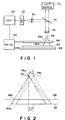
- Figure 1 is a schematic view of a known type alignment system utilizing zone plates.
- a parallel light emanating from a light source 72 passes through a half mirror 74 and is focused at a point 78 by a condensing lens 76. Thereafter, the light illuminates a mask alignment pattern 68a on a mask 68 and an alignment pattern 60a on a wafer 60 which is placed on a support table 62.
- Each of these alignment patterns 68a and 60a is provided by a reflection type zone plate and functions to form a spot of focused light on a plane perpendicular to an optical axis which contains the point 78. The amount of relative deviation of the positions of these light spots formed on that plane is detected, by directing the focused beams to a detection plane 82 by means of the condensing lens 76 and another lens 80.
- a control circuit 84 actuates a driving circuit 64 to relatively align the mask 68 and the wafer 60.
- Figure 2 illustrates an imaging relationship of lights from the mask alignment pattern 68a and the wafer alignment pattern 60a shown in Figure 1.
- a portion of the light divergently advancing from the point 78 is reflectively diffracted by the mask alignment pattern 68a and forms a spot 78a of focused light at or adjacent to the point 78, the spot representing the mask position.
- Another portion of the light passes through the mask 68 in the form of a zero-th order transmission light and is projected upon the wafer alignment pattern 60a on the wafer 60 surface with its wavefront being unchanged.
- the incident light is reflectively diffracted by the wafer alignment pattern 60a and then passes again through the mask 68 in the form of a zero-th order transmission light, and finally is focused in the neighborhood of the point 78 to form a spot 78b of focused light, representing the wafer position.
- the mask 68 functions merely as a transparent member.
- the position of the spot 78b formed by the wafer alignment pattern 60a in the described manner represents a deviation ⁇ , in the plane perpendicular to the optical axis containing the point 78, of an amount corresponding to the amount of deviation ⁇ of the wafer 60 with respect to the mask 68, in a direction (lateral direction) along the mask or wafer surface.
- Figure 3 is a schematic view of an interval measuring device such as proposed in Japanese Laid-Open Patent Application, Laid-Open no. 61-111402, wherein a mask (first object) M and a wafer (second object) W are disposed opposed to each other and, by means of a lens L1, light is focused at a point Ps which is between the mask M and the wafer W.
- the light from the lens L1 is reflected by the mask M surface and the wafer W surface, respectively and, through another lens L2, the reflected lights are projected on points Pw and Pm on a screen S surface, respectively.
- the interval between the mask M and the wafer W is detected by detecting the spacing between the convergent points Pw and Pm of the lights projected on the screen S surface.
- a coherent beam such as a laser beam is used to attain enhanced sensitivity.
- the inventors of the subject application have found specific inconveniences involved in these arrangement. Namely, as a consequence of use of a coherent beam, a speckle pattern (speckle noise) is produced by interference of scattered beams from the mask or wafer surface, and such speckle pattern is projected on the detection plane or a screen surface. Due to the superposition of such a speckle pattern on the light spot converged on the screen or detection plane, the intensity distribution of the light spot is disturbed which prevents accurate detection of the position of the light spot. This results in an error and in a degraded precision for the detection of a positional deviation or an interval of the mask and the wafer.
- a position detecting method wherein a radiation beam is projected to a pattern formed on a substrate and having an optical power at least with respect to a first direction, whereby the radiation beam is converged on a predetermined plane, and wherein the position of the substrate with respect to the first direction is determined on the basis of the position of the radiation beam upon the predetermined plane, the improvements residing in the steps of: relatively shifting the radiation beam and the substrate relative to each other in a second direction substantially orthogonal to the first direction, to thereby produce plural intensity distributions on the predetermined plane with the radiation beam; and determining the position of the substrate with respect to the first direction by using the produced intensity distributions.
- a height detecting method wherein a radiation beam is obliquely projected to a reflection surface of a substrate, whereby the radiation beam is reflected to a predetermined plane, and wherein the level of the reflection surface of the substrate is determined on the basis of the position of the radiation beam upon the predetermined plane, the improvements residing in the steps of: relatively shifting the radiation beam and the substrate relative to each other in a direction substantially orthogonal a plane of incidence of the radiation beam, to thereby produce plural intensity distributions on the predetermined plane with the radiation beam; and determining the level of the reflection surface of the substrate by using the produced intensity distributions.
- the position or level of a substrate may be determined in the present invention on the basis of (1) a gravity center position or a peak position of an intensity distribution to be defined by superposition of plural intensity distributions, or (2) gravity center positions or peak positions of plural intensity distributions, respectively.
- a CCD sensor means may be used to accumulate electric charges for the superposition of intensity distributions.
- An improved semiconductor device manufacturing method can be provided by the detection and correction of a positional deviation of a wafer with respect to a predetermined position, in accordance with an aspect of the present invention.
- an improved exposure apparatus can be provided by using a mechanism for detecting and correcting a positional deviation of a wafer with respect to a predetermined position, in accordance with an aspect of the present invention.
- Figures 1 and 2 are schematic views of a position detecting system of known type, using zone plates.
- Figure 3 is a schematic view of an interval measuring system of known type.
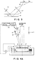
- Figure 4A is a schematic side sectional view of a main portion of an exposure apparatus into which a position detecting system according to a first embodiment of the present invention is incorporated.
- Figure 4B is an extended view of an optical arrangement of the position detecting system of the Figure 4A embodiment.
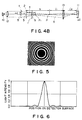
- Figure 5 is an enlarged top plan view of an alignment mark pattern used in the Figure 4A embodiment.
- Figures 6 and 7 are graphs each showing an intensity distribution of alignment light incident on a detector surface of Figure 4A.
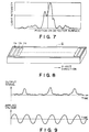
- Figure 8 is a perspective view schematically showing the detector of Figure 4A.
- Figure 9 is a timing chart, showing the relationship between an applied voltage to a driving means of the first embodiment and an output signal from the detector.
- Figures 10A, 10B and 10C are schematic views, respectively, showing a second embodiment of the present invention.
- Figures 11A and 11B are schematic views, respectively, showing a third embodiment of the present invention.
- Figure 12 is a schematic view for explaining relative shift of a light spot of alignment light and an alignment mark.
- Figure 13 is a block diagram, showing a modified form of the third embodiment of the present invention.
- Figures 4A and 4B show a position detecting system according to a first embodiment of the present invention, wherein Figure 4A is a sectional view of a main portion of an exposure apparatus into which the position detecting system of this embodiment is incorporated. In the case shown in Figure 4B, any positional deviation in respect to an X-axis direction is to be detected.
- the invention is applied to a semiconductor device manufacturing exposure apparatus of proximity type.
- Denoted at 1 is a mask (first object) having an electronic circuit pattern formed thereon, and denoted at 2 is a wafer (second object) onto which the circuit pattern of the mask is to be transferred with the use of an exposure beam.
- Denoted at 5 is an alignment mark formed on the mask 1 surface
- denoted at 3 is an alignment mark formed on the wafer 2 surface.
- Each of these alignment marks 5 and 3 is provided by a grating lens or a Fresnel zone plate, for example, having an optical power at least with respect to the positional deviation detecting direction (X-axis direction in this example) and having a one-dimensional or two-dimensional lens function.
- a relative positional deviation of the mask 1 and the wafer 2 with respect to the X-axis direction can be detected by using the light subjected to the wavefront transformation through the alignment marks 5 and 3.
- Figure 5 shows an example of mark pattern of the alignment mark 3 or 5 where a zone plate is used therefor.
- Denoted at 10 is a laser light source such as a semiconductor laser, which emits coherent light of good directivity.
- Light projecting lens 12 receives the laser light from the laser source 10 and transforms it into a parallel light which is then projected onto the alignment mark 5 on the mask 1 surface.
- Detector 11 comprises a CCD line sensor, for example.
- Light receiving lens 13 receives the light from the mask 1 surface and directs the same to the detector 11.
- the wafer 2 is placed on a wafer stage 13 which is driven by a stage driving means 18. By this stage driving means 18, the wafer stage 17 can be oscillated in Z-axis and/or Y-axis direction in this example, with short stroke, to be described later.
- Reference character E denotes the exposure range through which the exposure beam passes.
- the laser light from the laser source 10 is transformed by the light projecting lens 11 into a parallel light which is then incident on the alignment mark 5 on the mask 1 surface. Then, the light is subjected to the wavefront transformation (i.e. transmissive diffraction) through the alignment mark 5 and is inputted to the alignment mark 3 on the wafer 2 surface. Then, a portion of the light influenced by the optical function (i.e. reflective diffraction) of the alignment mark 3, goes through the mask 1 without being affected by the diffracting function of the alignment mark of the mask 1, and it is collected by the light receiving lens 13 and is incident on the light receiving surface of the detector 11 as "alignment light".
- the wavefront transformation i.e. transmissive diffraction
- the optical function i.e. reflective diffraction
- Figure 6 shows the intensity distribution of such an alignment light incident on the detector 11 surface.
- the alignment light incident on the detector 11 surface is photoelectrically converted into a signal of a waveform such as shown in Figure 3, which is outputted from the detector 11.
- the output signal from the detector 11 is analog-to-digital converted through an analog-to-digital converter (A/D converter) 19 into a digital signal which is applied to a computing means 20.
- the computing means 20 calculates the position of incidence (gravity center position) of the alignment light on the detector 11 and, from the detected position, it determines a relative positional deviation of the mask 1 and the wafer 2 in the X-axis direction (along the X-Y plane).
- the term "center of gravity of light” means such a point that, when on the light receiving surface of the detector a position vector of each point on that surface is multiplied by the light intensity of that point and the thus obtained products are integrated over the entire section, the integrated value has a "zero vector”.
- a peak point of light intensity may be used as a representative point.
- the light causing the speckle noise has a spot diameter approximately equal to that of the alignment light, when the same is superposed on the alignment light on the detector 11 surface, it can not be separated spatially or separated with respect to the spatial frequency, from the alignment light.
- At the time of detection of positional deviation at least one of the mask 1 and the wafer 2 is oscillatingly shifted by small amount relative to the incident beam (alignment light) in a non-sensitive direction (non-detecting direction), so as to attain spatial averaging of speckle noises (speckle patterns) produced by the relatively shifting scattered light and superposed on the alignment light.
- the wafer may be oscillatingly shifted by using the wafer driving means 18, in a direction (Z-axis direction) along which the wafer is opposed to the mask, and within a range of 1000 - 2000 angstroms.
- the detector 11 may comprise a number of light receiving elements (11a, 11b, 11c, ...) which are arrayed along the positional deviation detecting direction (X direction).
- the wafer 2 may be oscillated in a non-sensitive direction (i.e. Z direction in this example) so as not to affect against the positional deviation detection. Substantially the same advantageous effect is attainable by oscillating the wafer in the Y direction.
- the relative oscillation of the mask and/or the wafer dose not cause a change in the gravity center position of the alignment light with respect to the positional deviation detecting direction (X direction).
- X direction positional deviation detecting direction
- Figure 9 is a timing chart showing the relationship between the output signal from the detector and the electric voltage applied to the wafer driving means 18, where a piezoelectric device is used as the driving means 18 to oscillate the wafer stage 17 in the Y direction while a CCD sensor is used as the detector.
- a bimorph element may be used in the present invention as the wafer driving means 18, with substantially the same advantageous effects.
- the present invention is applicable also to a case where an error or deviation of the interval between the mask and the wafer, from a preset reference interval, is to be detected.
- Figure 10A is a schematic view of an optical arrangement of an embodiment of the present invention to be incorporated into a semiconductor device manufacturing exposure apparatus of proximity type, for measuring the interval between a mask and a wafer.
- Figures 10B and 10C are schematic views, respectively, each showing optical paths in a portion of Figure 10A.
- FIGs 10A - 10C only a mask, a wafer, optical systems and light receiving means are illustrated. Actually, however, the mask and the wafer are placed in an exposure apparatus such as shown in Figure 4A, and also the optical systems and the light receiving means are accommodated in such exposure apparatus.
- an output of the light receiving means is applied to a computing means such as at 20 in Figure 4A, and a driving means such as at 18 drives a wafer stage such as at 17 so as to oscillatingly shift the wafer in a Y direction, in this example, which is perpendicular to the plane of incidence (X-Z plane) of an input light obliquely incident on the wafer.
- denoted at 72 is a mask (first object); and denoted at 73 is a wafer (second object).
- the mask 72 and the wafer 73 are disposed opposed to each other, initially with a spacing d0.
- Denoted at 74 and 75 are first and second physical optic elements (alignment marks) each being formed on a scribe line on the mask 72 surface and each being provided by a diffraction grating, a zone plate or a Fresnel lens, for example.
- Light receiving means 78 comprises a line sensor or a PSD (position sensitive detector), for example, and it serves to detect the gravity center position of an incident light.
- Signal processing circuit 79 serves to process a signal from the light receiving means 78 to determine the gravity center position of the light incident on the detector 78 surface and also to calculate the interval between the mask 72 and the wafer 73 in the manner to be described later.
- Optical probe 80 includes the light receiving means 78 and, if necessary, the signal processing circuit 79, and it is relatively movable relative to the mask 72 or the wafer 73.
- Diffraction light of a predetermined order or orders, emanating from the first Fresnel zone plate 74 at an angle ⁇ 1, is reflected at a point B on the wafer 73 surface (at point C as the wafer 73 is at a position P2).
- reference numeral 31 denotes the reflection light from the wafer 73 as the same is at a reference position P1 close to the mask 72
- reference numeral 32 denotes the reflection light from the wafer as the same is at the position P2 displaced from the position P1 by a distance dG.
- the wafer 73 has no alignment mark but a reflective surface thereof is used.
- the reflection light from the wafer 73 is incident on a point D on a second Fresnel zone plate 75 on the mask (first object) 72 (or on a point E as the wafer 72 is at the position P2).
- the second Fresnel zone plate 75 has such optical function that, in response to the position of incidence of the input light thereon, the angle of emission of the diffraction light emanating therefrom changes.
- the detecting means 78 may comprise a CCD sensor, producing an output signal corresponding to an intensity distribution of a received light.
- the output signal from the detecting means is processed to determine the gravity center position of the light intensity distribution of the input light 61 (light 62 as the wafer 73 is at the position P2) incident on the light receiving means 78 surface, and from this, the interval between the mask 72 and the wafer 73 is determined by calculations. Then, the wafer stage 17 is moved upwardly or downwardly to adjust the interval of the mask and the wafer.
- Each of the first and second Fresnel zone plates 74 and 75 provided on the mask 72 has a preset pitch, and the angle ( ⁇ 1 or ⁇ 2) of diffraction of the light, of predetermined diffraction order or orders, incident on that zone plate is also preset.
- the interval d0 of the mask and the wafer as the wafer is at the position P1 may be set by using a separate measuring means.
- the driving means 18 oscillates the wafer 73 with a short stroke in a non-sensitive direction (i.e. Y direction), to the interval error detecting direction (Z direction).
- a non-sensitive direction i.e. Y direction
- the interval error detecting direction Z direction
- an input light beam is held fixed while, on the other hand, at least one of the mask and the wafer is oscillated in a non-sensitive direction, not affecting the position detection.
- a light source such as a laser having good coherency is used.
- further improvement of the detection precision is assured. Therefore, the present invention in these aspects assures a position detecting system by which a relative positional deviation of a mask and a wafer or a change in the interval therebetween can be detected very precisely.
- FIGS 11A and 11B show a third embodiment of the present invention. Since this embodiment has optical paths like those of the embodiment described with reference to Figure 4B, description of the present embodiment will be made also with reference to Figure 4B.
- the invention is applied to a semiconductor device manufacturing exposure apparatus of proximity exposure type.
- Denoted at 1 is a mask (first object) having an electronic circuit pattern formed thereon, and denoted at 2 is a wafer (second object).
- Denoted at 5 is an alignment mark formed on the mask 1 surface, and denoted at 3 is an alignment mark formed on the wafer 2 surface.
- Each of these alignment marks 5 and 3 is provided by a grating lens or a Fresnel zone plate, for example, having a one-dimensional or two-dimensional lens function, like the alignment marks of the mask and the wafer as described with reference to Figures 4A and 4B.
- a relative positional deviation of the mask 1 and the wafer 2 along the X-Y plane can be detected by using the light subjected to the wavefront transformation through the alignment marks 5 and 3.
- the alignment mark 3 or 5 may have a mark pattern such as shown in Figure 5 where a zone plate is used therefor.
- Denoted at 10 is a laser light source such as a semiconductor laser, which is driven by a driver 110 and which emits coherent light of good directivity.
- Collimator lens 12 receives the laser light from the laser source 10 and transforms it into a parallel light which is then projected onto a galvano mirror GM. This mirror can be oscillated with a short stroke to oscillatingly reflect a received light, whereby the alignment mark 5 on the mask 1 can be oscillatingly scanned with this light in a direction (Y direction in this example) perpendicular to the alignment direction (X direction in this example).
- Detector 11 comprises a CCD line sensor, for example.
- Light receiving lens 13 receives the light from the mask 1 surface and directs the same to the detector 11.
- the wafer 2 is placed on a wafer stage 17 which is driven by a stage driving means 18 and an actuator 22 such as a motor.
- the mirror GM is pivotally oscillated by small amount by driving means 21, about a rotational shaft which extends in parallel to the alignment direction (X direction) and which passes through the point of reflection on the mirror GM surface of the center beam of the light passed through the collimator lens 12.
- driving means 21 which extends in parallel to the alignment direction (X direction) and which passes through the point of reflection on the mirror GM surface of the center beam of the light passed through the collimator lens 12.
- the laser light from the laser source 10 is transformed by the collimator lens 11 into a parallel light which is then incident on mirror GM. Then, by the oscillation of the mirror GM, the alignment mark 5 of the mask 1 is scanned with the light from the mirror GM. Then, the light subjected to the wavefront transformation (i.e. transmissive diffraction) through the alignment mark 5 is inputted to the alignment mark 3 on the wafer 2 surface. Then, a portion of the light influenced by the wavefront transformation action (i.e. reflective diffraction) of the alignment mark 3, goes through the mask 1 without being affected by the diffracting function of the alignment mark of the mask 1, and it is collected by the light receiving lens 13 and is incident on the light receiving surface of the detector 11 as "alignnce light".
- the wavefront transformation i.e. transmissive diffraction
- Such an alignment light incident on the detector 11 surface has an intensity distribution such as shown in Figure 6.
- the alignment light incident on the detector 11 surface is then photoelectrically converted into a signal of a waveform such as shown in Figure 6, which is outputted from the detector 11.
- the output signal from the detector 11 is analog-to-digital converted through an analog-to-digital converter (A/D converter) 19 into a digital signal which is applied to a computing means 20.
- the computing means 20 processes the digital signal and calculates the position of incidence (gravity center position) of the alignment light on the detector 11 and, from the detected position, it determines a relative positional deviation of the mask 1 and the wafer 2 in the X-axis direction (along the X-Y plane).
- the stage driving means 18 moves the wafer stage 17 through the actuator 22, so as to align the mask 1 and the wafer 2 with each other.
- DH Denoted at DH in Figure 11B is a detection head in which the laser light source 10, the mirror GM and the detector 11 of Figure 11A are accommodated.
- the term "center of gravity of light” means such a point that, when on the light receiving surface of the detector a position vector of each point on that surface is multiplied by the light intensity of that point and the thus obtained products are integrated over the entire section, the integrated value has a "zero vector”.
- a peak point of light intensity may be used as a representative point.
- the light spot as formed by the alignment light 91 ( Figure 12) is oscillated by small amount to oscillatingly scan the alignment mark in a non-sensitive direction (Y direction in this example), so as to attain spatial averaging of speckle noises (speckle patterns) produced by the scattered light and superposed on the alignment light.
- the oscillation may be in a direction (Y-axis direction) perpendicular to the alignment direction (X-axis direction) and within a range of 1000 - 2000 angstroms.
- the detector 11 may comprise a number of light receiving elements (11a, 11b, 11c, ...) which are arrayed along the positional deviation detecting direction (X direction).
- the spot of the alignment light 91 may be oscillated in a non-sensitive direction (i.e. Y direction in this example).
- the amplitude of oscillation of the alignment light in this embodiment is determined by the diameter of the light in a direction perpendicular to the alignment direction, and this oscillation period is determined by the signal (charge) accumulation time period of the detecting means 11.
- each alignment mark has a size of several tens to several hundreds microns so that it can be provided on a scribe line which is defined to allow separation of chips printed in a matrix manner on one wafer.
- the diameter of the alignment light in a direction perpendicular to the alignment direction
- it is large enough to cover the alignment mark as a whole and, additionally, to assure that all the alignment mark area is continuously irradiated by the alignment light.
- it is not too large to assure that a sufficient light intensity of a level to be detected on the detecting means 11, is obtained. This is also with the case of the Figure 4A/4B embodiment or the Figure 10 embodiment.
- the amplitude of the small oscillation may preferably be several hundreds microns (maximum) and the oscillation period may be equal to a multiple, by an even number, of the accumulation time period of the detecting means.
- the alignment light is relatively oscillated by small amount relative to the mask and the wafer, in a direction (Y direction in this example) not affecting the position detection and, with this oscillation of the alignment light, the light intensity distribution of the speckle noise is averaged. Since the oscillation is in a direction perpendicular to and, thus, not affecting the position detection, it does not cause degradation of the detection precision. Therefore, high precision alignment is assured.
- an acousto-opticelement may be used as shown in Figure 13, with substantially the same advantageous effects.
- laser light source 13 is driven and controlled by a driving means 105, and the laser light from the source 13 is transformed by a collimator lens 102 into a parallel light which in turn is incident on an acousto-optic element 103.
- Driving means 104 controls the oscillation frequency to be applied to the acousto-optic element 103, and it controls the light (diffraction light) emanating from the element 103 by forming a phase grating within the element 103.
- the alignment light is oscillated on the surface of a mask or a wafer in a direction not affecting the position detection.
- the present invention assures a position detecting system by which any positional deviation of the mask and the wafer can be detected very precisely. Also, it is possible to reduce speckle noise without enlargement in structure of the device.
- an alignment beam and an article to be examined are relatively oscillated by small amount, within a charge accumulation time period of a light intensity detecting sensor such as CCD to thereby reduce the effect of speckle noise.
- the present invention is not limited to this form.
- the alignment beam and the article may be relatively oscillated with a period slower than the charge accumulation time period of the sensor and, from each of signals obtainable at certain time intervals, a corresponding quantity of positional deviation or a corresponding quantity of spacing (between the mask and the wafer) may be detected. Then, the obtained quantities of the positional deviation or the spacing may be averaged to determine the actual positional deviation or the actual spacing. Since in this example the speed of relative motion of the alignment beam and the article being examined in a direction not affecting the position detection, may be slow, it is not always necessary to use a piezoelectric device for the oscillation.
- the wafer 2 is oscillatingly moved
- the mask may be oscillated in place thereof.
- both of the mask and the wafer may be oscillated.
- an article to be examined may be oscillatingly moved while on the other hand an inspecting beam may be scanningly oscillated.
- the present invention is not limited to an exposure apparatus of proximity type, but is applicable also to a projection type exposure apparatus, en electron beam pattern drawing apparatus or a laser beam pattern drawing apparatus.
Landscapes
- Physics & Mathematics (AREA)
- General Physics & Mathematics (AREA)
- Engineering & Computer Science (AREA)
- Multimedia (AREA)
- Exposure And Positioning Against Photoresist Photosensitive Materials (AREA)
- Exposure Of Semiconductors, Excluding Electron Or Ion Beam Exposure (AREA)
Abstract

Description
- This invention relates to a method and device for optically detecting the position of an article very precisely. More particularly, the invention is concerned with a position detecting method and device suitably applicable to a semiconductor device manufacturing exposure apparatus, for example, for bringing a mask or a reticle and a wafer into a predetermined positional relationship before lithographically transferring a fine electronic circuit pattern of the mask or reticle onto the wafer.
- In exposure apparatuses for use in the manufacture of semiconductor devices, the relative alignment of a mask and a wafer and the setting of interval therebetween are important factors in respect to ensuring improved performance. Particularly, as for alignment and interval setting systems employed in recent exposure apparatuses, submicron alignment and interval setting accuracies or more strict accuracies are required in consideration of the demand for higher degree of integration of each semiconductor device.
- To this end, usually, the interval of a mask and a wafer is measured by using an interval measuring device and, after interval control to set a predetermined interval, the mask-to-wafer alignment is effected. In many types of alignment systems, features called "alignment patterns" are provided on a mask and a wafer and, by utilizing positional information obtainable from these patterns, the mask and wafer are aligned. As for the manner of executing the alignment, as an example there is a method wherein the amount of relative deviation of these alignment patterns is detected on the basis of image processing. Another method is proposed in U.S. Patent No. 4,037,969 or Japanese Laid-Open Patent Application, Laid-Open No. Sho 56-157033, wherein so-called zone plates are used as alignment patterns upon which light is projected and wherein the positions of light spots formed on a predetermined plane by lights from the illuminated zone plates are detected.
- Generally, an alignment method utilizing a zone plate is relatively insensitive to any defect of an alignment pattern and therefore assures relatively high alignment accuracies, as compared with an alignment method simply using a traditional alignment pattern.
- Figure 1 is a schematic view of a known type alignment system utilizing zone plates.
- In Figure 1, a parallel light emanating from a
light source 72 passes through ahalf mirror 74 and is focused at apoint 78 by acondensing lens 76. Thereafter, the light illuminates amask alignment pattern 68a on amask 68 and analignment pattern 60a on awafer 60 which is placed on a support table 62. Each of thesealignment patterns point 78. The amount of relative deviation of the positions of these light spots formed on that plane is detected, by directing the focused beams to adetection plane 82 by means of thecondensing lens 76 and anotherlens 80. - In accordance with an output signal from the
detector 82, acontrol circuit 84 actuates adriving circuit 64 to relatively align themask 68 and thewafer 60. - Figure 2 illustrates an imaging relationship of lights from the
mask alignment pattern 68a and thewafer alignment pattern 60a shown in Figure 1. - In Figure 2, a portion of the light divergently advancing from the
point 78 is reflectively diffracted by themask alignment pattern 68a and forms aspot 78a of focused light at or adjacent to thepoint 78, the spot representing the mask position. Another portion of the light passes through themask 68 in the form of a zero-th order transmission light and is projected upon thewafer alignment pattern 60a on thewafer 60 surface with its wavefront being unchanged. The incident light is reflectively diffracted by thewafer alignment pattern 60a and then passes again through themask 68 in the form of a zero-th order transmission light, and finally is focused in the neighborhood of thepoint 78 to form aspot 78b of focused light, representing the wafer position. In the illustrated example, when the light diffracted by thewafer 60 forms a spot, themask 68 functions merely as a transparent member. - The position of the
spot 78b formed by thewafer alignment pattern 60a in the described manner represents a deviation Δσ, in the plane perpendicular to the optical axis containing thepoint 78, of an amount corresponding to the amount of deviation Δσ of thewafer 60 with respect to themask 68, in a direction (lateral direction) along the mask or wafer surface. - Figure 3 is a schematic view of an interval measuring device such as proposed in Japanese Laid-Open Patent Application, Laid-Open no. 61-111402, wherein a mask (first object) M and a wafer (second object) W are disposed opposed to each other and, by means of a lens L1, light is focused at a point Ps which is between the mask M and the wafer W.
- Here, the light from the lens L1 is reflected by the mask M surface and the wafer W surface, respectively and, through another lens L2, the reflected lights are projected on points Pw and Pm on a screen S surface, respectively. The interval between the mask M and the wafer W is detected by detecting the spacing between the convergent points Pw and Pm of the lights projected on the screen S surface.
- In the above-described arrangements, usually a coherent beam such as a laser beam is used to attain enhanced sensitivity. The inventors of the subject application have found specific inconveniences involved in these arrangement. Namely, as a consequence of use of a coherent beam, a speckle pattern (speckle noise) is produced by interference of scattered beams from the mask or wafer surface, and such speckle pattern is projected on the detection plane or a screen surface. Due to the superposition of such a speckle pattern on the light spot converged on the screen or detection plane, the intensity distribution of the light spot is disturbed which prevents accurate detection of the position of the light spot. This results in an error and in a degraded precision for the detection of a positional deviation or an interval of the mask and the wafer.
- It is accordingly a primary object of the present invention to provide an improved method or device for detecting the position or level (height) of an article very precisely.
- It is another object of the present invention to provide an improved alignment and exposure method or apparatus for manufacture of semiconductor devices which uses such a position detecting method and device.
- In accordance with a first aspect of the present invention, there is probided a position detecting method wherein a radiation beam is projected to a pattern formed on a substrate and having an optical power at least with respect to a first direction, whereby the radiation beam is converged on a predetermined plane, and wherein the position of the substrate with respect to the first direction is determined on the basis of the position of the radiation beam upon the predetermined plane, the improvements residing in the steps of: relatively shifting the radiation beam and the substrate relative to each other in a second direction substantially orthogonal to the first direction, to thereby produce plural intensity distributions on the predetermined plane with the radiation beam; and determining the position of the substrate with respect to the first direction by using the produced intensity distributions.
- In accordance with a second aspect of the present invention, there is provided a height detecting method wherein a radiation beam is obliquely projected to a reflection surface of a substrate, whereby the radiation beam is reflected to a predetermined plane, and wherein the level of the reflection surface of the substrate is determined on the basis of the position of the radiation beam upon the predetermined plane, the improvements residing in the steps of: relatively shifting the radiation beam and the substrate relative to each other in a direction substantially orthogonal a plane of incidence of the radiation beam, to thereby produce plural intensity distributions on the predetermined plane with the radiation beam; and determining the level of the reflection surface of the substrate by using the produced intensity distributions.
- The position or level of a substrate may be determined in the present invention on the basis of (1) a gravity center position or a peak position of an intensity distribution to be defined by superposition of plural intensity distributions, or (2) gravity center positions or peak positions of plural intensity distributions, respectively. When the method (1) is to be used, preferably a CCD sensor means may be used to accumulate electric charges for the superposition of intensity distributions.
- An improved semiconductor device manufacturing method can be provided by the detection and correction of a positional deviation of a wafer with respect to a predetermined position, in accordance with an aspect of the present invention.
- Also, an improved exposure apparatus can be provided by using a mechanism for detecting and correcting a positional deviation of a wafer with respect to a predetermined position, in accordance with an aspect of the present invention.
- These and other objects, features and advantages of the present invention will become more apparent upon a consideration of the following description of the preferred embodiments of the present invention taken in conjunction with the accompanying drawings.
- Figures 1 and 2 are schematic views of a position detecting system of known type, using zone plates.
- Figure 3 is a schematic view of an interval measuring system of known type.
- Figure 4A is a schematic side sectional view of a main portion of an exposure apparatus into which a position detecting system according to a first embodiment of the present invention is incorporated.
- Figure 4B is an extended view of an optical arrangement of the position detecting system of the Figure 4A embodiment.
- Figure 5 is an enlarged top plan view of an alignment mark pattern used in the Figure 4A embodiment.
- Figures 6 and 7 are graphs each showing an intensity distribution of alignment light incident on a detector surface of Figure 4A.
- Figure 8 is a perspective view schematically showing the detector of Figure 4A.
- Figure 9 is a timing chart, showing the relationship between an applied voltage to a driving means of the first embodiment and an output signal from the detector.
- Figures 10A, 10B and 10C are schematic views, respectively, showing a second embodiment of the present invention.
- Figures 11A and 11B are schematic views, respectively, showing a third embodiment of the present invention.
- Figure 12 is a schematic view for explaining relative shift of a light spot of alignment light and an alignment mark.
- Figure 13 is a block diagram, showing a modified form of the third embodiment of the present invention.
- Figures 4A and 4B show a position detecting system according to a first embodiment of the present invention, wherein Figure 4A is a sectional view of a main portion of an exposure apparatus into which the position detecting system of this embodiment is incorporated. In the case shown in Figure 4B, any positional deviation in respect to an X-axis direction is to be detected. In this embodiment, the invention is applied to a semiconductor device manufacturing exposure apparatus of proximity type.
- Denoted at 1 is a mask (first object) having an electronic circuit pattern formed thereon, and denoted at 2 is a wafer (second object) onto which the circuit pattern of the mask is to be transferred with the use of an exposure beam. Through this exposure and transfer process, semiconductor devices can be manufactured from the wafer. Denoted at 5 is an alignment mark formed on the
mask 1 surface, and denoted at 3 is an alignment mark formed on thewafer 2 surface. Each of thesealignment marks - In this embodiment, a relative positional deviation of the
mask 1 and thewafer 2 with respect to the X-axis direction can be detected by using the light subjected to the wavefront transformation through thealignment marks alignment mark - Denoted at 10 is a laser light source such as a semiconductor laser, which emits coherent light of good directivity.
Light projecting lens 12 receives the laser light from thelaser source 10 and transforms it into a parallel light which is then projected onto thealignment mark 5 on themask 1 surface. Detector 11 comprises a CCD line sensor, for example.Light receiving lens 13 receives the light from themask 1 surface and directs the same to the detector 11. Thewafer 2 is placed on awafer stage 13 which is driven by a stage driving means 18. By this stage driving means 18, thewafer stage 17 can be oscillated in Z-axis and/or Y-axis direction in this example, with short stroke, to be described later. Reference character E denotes the exposure range through which the exposure beam passes. - In this embodiment, the laser light from the
laser source 10 is transformed by the light projecting lens 11 into a parallel light which is then incident on thealignment mark 5 on themask 1 surface. Then, the light is subjected to the wavefront transformation (i.e. transmissive diffraction) through thealignment mark 5 and is inputted to thealignment mark 3 on thewafer 2 surface. Then, a portion of the light influenced by the optical function (i.e. reflective diffraction) of thealignment mark 3, goes through themask 1 without being affected by the diffracting function of the alignment mark of themask 1, and it is collected by thelight receiving lens 13 and is incident on the light receiving surface of the detector 11 as "alignment light". - Figure 6 shows the intensity distribution of such an alignment light incident on the detector 11 surface. The alignment light incident on the detector 11 surface is photoelectrically converted into a signal of a waveform such as shown in Figure 3, which is outputted from the detector 11. The output signal from the detector 11 is analog-to-digital converted through an analog-to-digital converter (A/D converter) 19 into a digital signal which is applied to a computing means 20. In response, the computing means 20 calculates the position of incidence (gravity center position) of the alignment light on the detector 11 and, from the detected position, it determines a relative positional deviation of the
mask 1 and thewafer 2 in the X-axis direction (along the X-Y plane). - Assuming now that the
mask 1 and thewafer 2 have a relative deviation Δσ in the X direction as shown in Figure 4B, that the distance from thewafer 2 to the point P1 of light convergence as determined by the focal length of themask alignment mark 5 is a, that the distance to the point P2 of convergence of the light reflectively diffracted by thewafer alignment mark 3 and passing through themask alignment mark 5 is b, and that thelens 13 has a unit imaging magnification (= 1x), then on the detector 11 surface there occurs a displacement Δδ of the gravity center of the spot of converged alignment light S which can be expressed as follows:
- If a = 0.5 mm and b = 50 mm, then from equation (1) the positional deviation is magnified by 101x.
- Here, as seen from equation (1), there is a proportional relationship between the positional deviation Δσ and the displacement Δδ of the gravity center position. If the detecting means (11, 19, 20) has a resolution of 0.1 micron, then the resolution for the positional deviation Δσ is 0.001 micron.
- In this embodiment, the term "center of gravity of light" means such a point that, when on the light receiving surface of the detector a position vector of each point on that surface is multiplied by the light intensity of that point and the thus obtained products are integrated over the entire section, the integrated value has a "zero vector". As an alternative, a peak point of light intensity may be used as a representative point.
- Details of the principle of the positional deviation detection as described above and used in this embodiment of the present invention, are explained in Japanese Laid-Open Patent Application No. 01-233305 or No. 02-1506 filed in Japan in the name of the assignee of the subject application.
- Important features of this embodiment of the present invention will now be explained.
- Generally, if a laser beam is incident on a portion of the mask surface having a small surface irregularity or on an aluminum-coated portion of the wafer surface having a small surface irregularity (1000 angstroms or less), there occurs scattering of light which causes speckle noise to be superposed on the alignment light upon the detector 11 surface. The intensity of such speckle noise resulting from the scattered light is higher with larger coherency of a laser light source used, and the intensity distribution of the speckle noise changes in dependence upon the relative position of the wafer to the mask or the interval between the mask and the wafer. Unless there occurs a relative change in the
laser light source 10, in themask 1 or in thewafer 2, such noise light does not change and, thus, even the electrical averaging with time does not effectively avoid the noise light. - Further, since the light causing the speckle noise has a spot diameter approximately equal to that of the alignment light, when the same is superposed on the alignment light on the detector 11 surface, it can not be separated spatially or separated with respect to the spatial frequency, from the alignment light.
- This results in disturbance of the waveform of the output signal from the detector 11, such as shown in Figure 7, and in a shift of the gravity center position of the incident light on the detector 11 surface, causing an error in the detection of the positional deviation.
- Particular attentions have been paid to this in the present invention and, in this embodiment, at the time of detection of positional deviation, at least one of the
mask 1 and thewafer 2 is oscillatingly shifted by small amount relative to the incident beam (alignment light) in a non-sensitive direction (non-detecting direction), so as to attain spatial averaging of speckle noises (speckle patterns) produced by the relatively shifting scattered light and superposed on the alignment light. - As an example, the wafer may be oscillatingly shifted by using the wafer driving means 18, in a direction (Z-axis direction) along which the wafer is opposed to the mask, and within a range of 1000 - 2000 angstroms. As shown in Figure 8, the detector 11 may comprise a number of light receiving elements (11a, 11b, 11c, ...) which are arrayed along the positional deviation detecting direction (X direction). Thus, at the time of positional deviation detection, the
wafer 2 may be oscillated in a non-sensitive direction (i.e. Z direction in this example) so as not to affect against the positional deviation detection. Substantially the same advantageous effect is attainable by oscillating the wafer in the Y direction. - The relative oscillation of the mask and/or the wafer dose not cause a change in the gravity center position of the alignment light with respect to the positional deviation detecting direction (X direction). Thus, by averaging with time the output signals (waveforms) from the detector 11, it is possible to prevent unwanted shift of the gravity center position of the alignment light due to the speckle noise and to avoid an error in the positional deviation detection. On the basis of the positional deviation detected, it is possible to correctly align the mask and the wafer to remove their relative positional deviation.
- Figure 9 is a timing chart showing the relationship between the output signal from the detector and the electric voltage applied to the wafer driving means 18, where a piezoelectric device is used as the driving means 18 to oscillate the
wafer stage 17 in the Y direction while a CCD sensor is used as the detector. - It is seen from Figure 9 that the electric charges produced in response to the alignment light and the speckle noise during oscillation of the
stage 17 by the piezoelectric device, are accumulated by the CCD and the accumulated charges are outputted as a single output signal. This reduces the effect of the speckle noise (the intensity distribution of the speckle noise is averaged into an approximately flat distribution) and, therefore, it is possible to obtain a signal that correctly represents the relative position of the mask and the wafer. The charge accumulation time of the CCD (signal output timing) can be appropriately set by using a CCD driver. - A bimorph element may be used in the present invention as the wafer driving means 18, with substantially the same advantageous effects.
- While in the above-described embodiment the invention has been explained with reference to a case where a positional deviation of a mask and a wafer along the X-Y plane is detected and corrected, the present invention is applicable also to a case where an error or deviation of the interval between the mask and the wafer, from a preset reference interval, is to be detected.
- Figure 10A is a schematic view of an optical arrangement of an embodiment of the present invention to be incorporated into a semiconductor device manufacturing exposure apparatus of proximity type, for measuring the interval between a mask and a wafer. Figures 10B and 10C are schematic views, respectively, each showing optical paths in a portion of Figure 10A.
- In Figures 10A - 10C, only a mask, a wafer, optical systems and light receiving means are illustrated. Actually, however, the mask and the wafer are placed in an exposure apparatus such as shown in Figure 4A, and also the optical systems and the light receiving means are accommodated in such exposure apparatus. Thus, an output of the light receiving means is applied to a computing means such as at 20 in Figure 4A, and a driving means such as at 18 drives a wafer stage such as at 17 so as to oscillatingly shift the wafer in a Y direction, in this example, which is perpendicular to the plane of incidence (X-Z plane) of an input light obliquely incident on the wafer.
- In Figures 10A - 10C, denoted at 71 is a coherent light emanating from a coherent light source LD such as a He-Ne laser or a semiconductor laser, for example; denoted at 72 is a mask (first object); and denoted at 73 is a wafer (second object). The
mask 72 and thewafer 73 are disposed opposed to each other, initially with a spacing d0. Denoted at 74 and 75 are first and second physical optic elements (alignment marks) each being formed on a scribe line on themask 72 surface and each being provided by a diffraction grating, a zone plate or a Fresnel lens, for example. - Light receiving means 78 comprises a line sensor or a PSD (position sensitive detector), for example, and it serves to detect the gravity center position of an incident light.
Signal processing circuit 79 serves to process a signal from the light receiving means 78 to determine the gravity center position of the light incident on thedetector 78 surface and also to calculate the interval between themask 72 and thewafer 73 in the manner to be described later.Optical probe 80 includes the light receiving means 78 and, if necessary, thesignal processing circuit 79, and it is relatively movable relative to themask 72 or thewafer 73. - In this embodiment, the light (wavelength λ = 830 nm) 71 from a semiconductor laser LD is incident on a point A on a Fresnel zone plate (first physical optic element) 74 provided on the
mask 72, whereby the incident light is diffracted. Diffraction light of a predetermined order or orders, emanating from the firstFresnel zone plate 74 at an angle ϑ1, is reflected at a point B on thewafer 73 surface (at point C as thewafer 73 is at a position P2). In Figure 10A,reference numeral 31 denotes the reflection light from thewafer 73 as the same is at a reference position P1 close to themask 72, whilereference numeral 32 denotes the reflection light from the wafer as the same is at the position P2 displaced from the position P1 by a distance dG. In this embodiment, thewafer 73 has no alignment mark but a reflective surface thereof is used. - Then, the reflection light from the
wafer 73 is incident on a point D on a secondFresnel zone plate 75 on the mask (first object) 72 (or on a point E as thewafer 72 is at the position P2). The secondFresnel zone plate 75 has such optical function that, in response to the position of incidence of the input light thereon, the angle of emission of the diffraction light emanating therefrom changes. -
Diffraction light 61 of a predetermined order or orders emanating from the secondFresnel zone plate 75 at an angle ϑ2 (ordiffraction light 62 as thewafer 73 is at the position P2), is incident on the detecting means 78 surface. The detecting means 78 may comprise a CCD sensor, producing an output signal corresponding to an intensity distribution of a received light. - The output signal from the detecting means is processed to determine the gravity center position of the light intensity distribution of the input light 61 (
light 62 as thewafer 73 is at the position P2) incident on the light receiving means 78 surface, and from this, the interval between themask 72 and thewafer 73 is determined by calculations. Then, thewafer stage 17 is moved upwardly or downwardly to adjust the interval of the mask and the wafer. - Each of the first and second
Fresnel zone plates mask 72 has a preset pitch, and the angle (ϑ1 or ϑ2) of diffraction of the light, of predetermined diffraction order or orders, incident on that zone plate is also preset. - Assuming now that the second
Fresnel zone plate 75 has a focal length of fM2 (micron), while it may be either positive or negative, and that the distance from the secondFresnel zone plate 75 to a light evaluation plane equivalent to the detecting means 78 surface is ℓ, then displacement S of the gravity center position of the light on the light receiving means 78 surface, from the position as assumed when thewafer 73 is at its reference position P1, to be caused in response to the shift of thewafer 73 from the reference position P1 by a distance dG, is given by the following equation:
wafer 73 is at the reference position P1 can be detected beforehand. Thus, by detecting during actual interval measurement a displacement of the gravity center position from the reference point and by substituting the detected displacement S into equation (2), it is possible to determine the displacement dG of thewafer 73 from the position P1, in the direction of the interval. - The interval d0 of the mask and the wafer as the wafer is at the position P1 may be set by using a separate measuring means.
- In this embodiment, like the first embodiment, for avoiding the adverse effect of the noise light due to speckle scattered light, within the charge accumulation time of the light receiving means 78 the driving means 18 oscillates the
wafer 73 with a short stroke in a non-sensitive direction (i.e. Y direction), to the interval error detecting direction (Z direction). By using a signal thus obtained, high precision interval measurement is assured. - In the embodiments described hereinbefore, an input light beam is held fixed while, on the other hand, at least one of the mask and the wafer is oscillated in a non-sensitive direction, not affecting the position detection. This effectively avoids the adverse effect of speckle noise resulting from the light scatted by an irregular surface portion of the mask or the wafer, where a light source such as a laser having good coherency is used. Also, based on the averaging effect, further improvement of the detection precision is assured. Therefore, the present invention in these aspects assures a position detecting system by which a relative positional deviation of a mask and a wafer or a change in the interval therebetween can be detected very precisely.
- Figures 11A and 11B show a third embodiment of the present invention. Since this embodiment has optical paths like those of the embodiment described with reference to Figure 4B, description of the present embodiment will be made also with reference to Figure 4B.
- In the present embodiment, the invention is applied to a semiconductor device manufacturing exposure apparatus of proximity exposure type.
- Denoted at 1 is a mask (first object) having an electronic circuit pattern formed thereon, and denoted at 2 is a wafer (second object). Denoted at 5 is an alignment mark formed on the
mask 1 surface, and denoted at 3 is an alignment mark formed on thewafer 2 surface. Each of thesealignment marks - In this embodiment, like the Figure 4A/4B embodiment, a relative positional deviation of the
mask 1 and thewafer 2 along the X-Y plane can be detected by using the light subjected to the wavefront transformation through the alignment marks 5 and 3. Thus, thealignment mark - Denoted at 10 is a laser light source such as a semiconductor laser, which is driven by a
driver 110 and which emits coherent light of good directivity.Collimator lens 12 receives the laser light from thelaser source 10 and transforms it into a parallel light which is then projected onto a galvano mirror GM. This mirror can be oscillated with a short stroke to oscillatingly reflect a received light, whereby thealignment mark 5 on themask 1 can be oscillatingly scanned with this light in a direction (Y direction in this example) perpendicular to the alignment direction (X direction in this example). Detector 11 comprises a CCD line sensor, for example.Light receiving lens 13 receives the light from themask 1 surface and directs the same to the detector 11. Thewafer 2 is placed on awafer stage 17 which is driven by a stage driving means 18 and anactuator 22 such as a motor. - In this embodiment, the mirror GM is pivotally oscillated by small amount by driving
means 21, about a rotational shaft which extends in parallel to the alignment direction (X direction) and which passes through the point of reflection on the mirror GM surface of the center beam of the light passed through thecollimator lens 12. With the light from the mirror GM, a light spot is formed on themask 1 surface and, this light spot is scanningly oscillated at a predetermined amplitude and a predetermined period. - In this embodiment, the laser light from the
laser source 10 is transformed by the collimator lens 11 into a parallel light which is then incident on mirror GM. Then, by the oscillation of the mirror GM, thealignment mark 5 of themask 1 is scanned with the light from the mirror GM. Then, the light subjected to the wavefront transformation (i.e. transmissive diffraction) through thealignment mark 5 is inputted to thealignment mark 3 on thewafer 2 surface. Then, a portion of the light influenced by the wavefront transformation action (i.e. reflective diffraction) of thealignment mark 3, goes through themask 1 without being affected by the diffracting function of the alignment mark of themask 1, and it is collected by thelight receiving lens 13 and is incident on the light receiving surface of the detector 11 as "alignmment light". - Such an alignment light incident on the detector 11 surface has an intensity distribution such as shown in Figure 6. The alignment light incident on the detector 11 surface is then photoelectrically converted into a signal of a waveform such as shown in Figure 6, which is outputted from the detector 11. The output signal from the detector 11 is analog-to-digital converted through an analog-to-digital converter (A/D converter) 19 into a digital signal which is applied to a computing means 20. In response, the computing means 20 processes the digital signal and calculates the position of incidence (gravity center position) of the alignment light on the detector 11 and, from the detected position, it determines a relative positional deviation of the
mask 1 and thewafer 2 in the X-axis direction (along the X-Y plane). - In response to the signal from the computing means 20, the stage driving means 18 (Figure 11B) moves the
wafer stage 17 through theactuator 22, so as to align themask 1 and thewafer 2 with each other. This is also with the case of the Figure 4A/4B embodiment. Denoted at DH in Figure 11B is a detection head in which thelaser light source 10, the mirror GM and the detector 11 of Figure 11A are accommodated. - Assuming now that the
mask 1 and thewafer 2 have a relative deviation Δσ in the X direction as shown in Figure 4B, that the distance from thewafer 2 to the point P1 of light convergence as determined by the focal length of themask alignment mark 5 is a, that the distance to the point P2 of convergence of the light reflectively diffracted by thewafer alignment mark 3 and passing through themask alignment mark 5 is b, and that thelens 13 has a unit imaging magnification (= 1x), then on the detector 11 surface there occurs a displacement Δδ of the gravity center of the spot of converged alignment light S which can be expressed by equation (1) set forth hereinbefore. Thus, on the detector 11 surface, the positional deviation Δσ is magnified by "b/a + 1". - If a = 0.5 mm and b = 50 mm, then from equation (1) the positional deviation Δσ is magnified by 101x.
- Here, as seen from equation (1), there is a proportional relationship between the positional deviation Δσ and the displacement Δσ of the gravity center position. If the detecting means (11, 19, 20) has a resolution of 0.1 micron, then the resolution for the positional deviation Δσ is 0.001 micron.
- In this embodiment, the term "center of gravity of light" means such a point that, when on the light receiving surface of the detector a position vector of each point on that surface is multiplied by the light intensity of that point and the thus obtained products are integrated over the entire section, the integrated value has a "zero vector". As an alternative, a peak point of light intensity may be used as a representative point.
- Important features of this embodiment of the present invention will now be explained.
- Generally, if a laser beam is incident on a portion of the mask surface having a small surface irregularity or on an aluminum-coated portion of the wafer surface having a small surface irregularity (1000 angstroms or less), there occurs scattering of light which causes speckle noise to be superposed on the alignment light upon the detector 11 surface. The intensity of such speckle noise resulting from the scattered light is higher with larger coherency of a laser light source used, and the intensity distribution of the speckle noise changes in dependence upon the relative position of the wafer to the mask or the interval between the mask and the wafer.
- This results in disturbance of the waveform of the output signal from the detector 11, such as shown in Figure 7, and in an apparent shift of the gravity center position of the incident light on the detector 11 surface, causing an error in the detection of the positional deviation.
- Particular attentions have been paid to this in the present invention and, in this embodiment, at the time of detection of positional deviation and within a preset accumulation time period of the detecting means, the light spot as formed by the alignment light 91 (Figure 12) is oscillated by small amount to oscillatingly scan the alignment mark in a non-sensitive direction (Y direction in this example), so as to attain spatial averaging of speckle noises (speckle patterns) produced by the scattered light and superposed on the alignment light.
- As an example, the oscillation may be in a direction (Y-axis direction) perpendicular to the alignment direction (X-axis direction) and within a range of 1000 - 2000 angstroms.
- As shown in Figure 8, the detector 11 may comprise a number of light receiving elements (11a, 11b, 11c, ...) which are arrayed along the positional deviation detecting direction (X direction). Thus, at the time of positional deviation detection, the spot of the
alignment light 91 may be oscillated in a non-sensitive direction (i.e. Y direction in this example). - The amplitude of oscillation of the alignment light in this embodiment is determined by the diameter of the light in a direction perpendicular to the alignment direction, and this oscillation period is determined by the signal (charge) accumulation time period of the detecting means 11.
- Generally, each alignment mark has a size of several tens to several hundreds microns so that it can be provided on a scribe line which is defined to allow separation of chips printed in a matrix manner on one wafer. Thus, as regards the the diameter of the alignment light (in a direction perpendicular to the alignment direction), preferably it is large enough to cover the alignment mark as a whole and, additionally, to assure that all the alignment mark area is continuously irradiated by the alignment light. Simultaneously therewith, preferably it is not too large to assure that a sufficient light intensity of a level to be detected on the detecting means 11, is obtained. This is also with the case of the Figure 4A/4B embodiment or the Figure 10 embodiment.
- In the present embodiment and in the embodiments described with reference to Figures 4A, 4B, and 10, the amplitude of the small oscillation may preferably be several hundreds microns (maximum) and the oscillation period may be equal to a multiple, by an even number, of the accumulation time period of the detecting means.
- In this embodiment, as best seen in Figure 12, the alignment light is relatively oscillated by small amount relative to the mask and the wafer, in a direction (Y direction in this example) not affecting the position detection and, with this oscillation of the alignment light, the light intensity distribution of the speckle noise is averaged. Since the oscillation is in a direction perpendicular to and, thus, not affecting the position detection, it does not cause degradation of the detection precision. Therefore, high precision alignment is assured.
- Where a piezoelectric device is used as the driving means 21 for the mirror GM to oscillate the alignment light and where a CCD sensor is used as the detecting means 11, the relationship between the voltage to be applied to the piezoelectric device and the output signal from the detecting means is such as shown in Figure 9.
- While this embodiment uses a galvano mirror for oscillation of the alignment light, an acousto-opticelement (AO) may be used as shown in Figure 13, with substantially the same advantageous effects.
- In Figure 13,
laser light source 13 is driven and controlled by a driving means 105, and the laser light from thesource 13 is transformed by acollimator lens 102 into a parallel light which in turn is incident on an acousto-optic element 103. Driving means 104 controls the oscillation frequency to be applied to the acousto-optic element 103, and it controls the light (diffraction light) emanating from theelement 103 by forming a phase grating within theelement 103. - In this example, only light L1 of first order is used and, therefore, the other lights such as zero-th order light L0 and second order light L2 are intercepted by a blocking
plate 106. By periodically changing the oscillation frequency to be applied by the driving means 104 to the acousto-optic element 103, the first order light L1 emanating therefrom is oscillated by small amount. - In these embodiments of the present invention, the alignment light is oscillated on the surface of a mask or a wafer in a direction not affecting the position detection. This assuredly avoids the adverse effects of speckle noise resulting from scattered light from an irregular surface portion of a mask or a wafer in a case where a laser light having good coherency is used as a light source means. Owing to this and to the resultant averaging effect as described, the present invention assures a position detecting system by which any positional deviation of the mask and the wafer can be detected very precisely. Also, it is possible to reduce speckle noise without enlargement in structure of the device.
- In the embodiments of the present invention as described hereinbefore, an alignment beam and an article to be examined are relatively oscillated by small amount, within a charge accumulation time period of a light intensity detecting sensor such as CCD to thereby reduce the effect of speckle noise. However, the present invention is not limited to this form. As an example, the alignment beam and the article may be relatively oscillated with a period slower than the charge accumulation time period of the sensor and, from each of signals obtainable at certain time intervals, a corresponding quantity of positional deviation or a corresponding quantity of spacing (between the mask and the wafer) may be detected. Then, the obtained quantities of the positional deviation or the spacing may be averaged to determine the actual positional deviation or the actual spacing. Since in this example the speed of relative motion of the alignment beam and the article being examined in a direction not affecting the position detection, may be slow, it is not always necessary to use a piezoelectric device for the oscillation.
- Further, while in the Figure 4A/4B embodiment the
wafer 2 is oscillatingly moved, the mask may be oscillated in place thereof. Alternatively, both of the mask and the wafer may be oscillated. As a further alternative, an article to be examined may be oscillatingly moved while on the other hand an inspecting beam may be scanningly oscillated. - Also, clearly the present invention is applicable to a system such as shown in Figure 1, 2 or 3.
- Moreover, the present invention is not limited to an exposure apparatus of proximity type, but is applicable also to a projection type exposure apparatus, en electron beam pattern drawing apparatus or a laser beam pattern drawing apparatus.
- While the invention has been described with reference to the structures disclosed herein, it is not confined to the details set forth and this application is intended to cover such modifications or changes as may come within the purposes of the improvements or the scope of the following claims.
Claims (30)
- In a position detecting method wherein a radiation beam is projected to a pattern formed on a substrate and having an optical power at least with respect to a first direction, whereby the radiation beam is converged on a predetermined plane, and wherein the position of the substrate with respect to the first direction is determined on the basis of the position of the radiation beam upon the predetermined plane, the improvements residing in the steps of:
relatively shifting the radiation beam and the substrate relative to each other in a second direction substantially orthogonal to the first direction, to thereby produce plural intensity distributions on the predetermined plane with the radiation beam; and
determining the position of the substrate with respect to the first direction by using the produced intensity distributions. - A method according to Claim 1, wherein the radiation beam and the substrate are relatively oscillated in the second direction.
- A method according to Claim 2, wherein, for said relative shifting, the substrate is displaced in the second direction.
- A method according to Claim 2, wherein, for said relative shifting, the radiation beam is displaced in the second direction.
- A method according to Claim 2, wherein the second direction is substantially parallel to the surface of the substrate.
- A method according to Claim 2, wherein the second direction is substantially perpendicular to the surface of the substrate.
- A method according to Claim 1, wherein said position determination is based on a gravity center position of superposed intensity distributions.
- A method according to Claim 1, wherein said position determination is based on gravity center positions of the plural intensity distributions, respectively.
- In a height detecting method wherein a radiation beam is obliquely projected to a reflection surface of a substrate, whereby the radiation beam is reflected to a predetermined plane, and wherein the level of the reflection surface of the substrate is determined on the basis of the position of the radiation beam upon the predetermined plane, the improvements residing in the steps of:
relatively shifting the radiation beam and the substrate relative to each other in a direction substantially orthogonal a plane of incidence of the radiation beam, to thereby produce plural intensity distributions on the predetermined plane with the radiation beam; and
determining the level of the reflection surface of the substrate by using the produced intensity distributions. - A method according to Claim 9, wherein the radiation beam and the substrate are relatively oscillated in the second direction.
- A method according to Claim 10, wherein, for said relative shifting, the substrate is displaced in the second direction.
- A method according to Claim 10, wherein, for said relative shifting, the radiation beam is displaced in the second direction.
- A method according to Claim 9, wherein said level determination is based on a gravity center position of superposed intensity distributions.
- A method according to Claim 9, wherein said level determination is based on gravity center positions of the plural intensity distributions, respectively.
- In a semiconductor device manufacturing method wherein a radiation beam is projected to a pattern formed on a substrate and having an optical power at least with respect to a first direction, whereby the radiation beam is converged on a predetermined plane, wherein a positional deviation of the substrate with respect to the first direction is determined on the basis of the position of the radiation beam upon the predetermined plane, and wherein, after correction of the positional deviation, a circuit pattern is printed on the substrate for the semiconductor device manufacture, the improvements residing in the steps of:
relatively shifting the radiation beam and the substrate relative to each other in a second direction orthogonal to the first direction, to thereby produce plural intensity distributions on the predetermined plane with the radiation beam; and
determining the positional deviation of the substrate with respect to the first direction by using the produced intensity distributions. - A method according to Claim 15, wherein the radiation beam and the substrate are relatively oscillated in the second direction.
- A method according to Claim 16, wherein, for said relative shifting, the substrate is displaced in the second direction.
- A method according to Claim 16, wherein, for said relative shifting, the radiation beam is displaced in the second direction.
- A method according to Claim 16, wherein the second direction is substantially parallel to the surface of the substrate.
- A method according to Claim 16, wherein the second direction is substantially perpendicular to the surface of the substrate.
- A method according to Claim 15, wherein said position determination is based on a gravity center position of superposed intensity distributions.
- A method according to Claim 15, wherein said position determination is based on gravity center positions of the plural intensity distributions, respectively.
- In a semiconductor device manufacturing method wherein a radiation beam is obliquely projected to a surface of a substrate, whereby the radiation beam is reflected to a predetermined plane, wherein the level of the surface of the substrate is determined on the basis of the position of the radiation beam upon the predetermined plane, and wherein, after adjustment of the level of the surface of the substrate, a circuit pattern is printed on the substrate for the semiconductor device manufacture, the improvements residing in the steps of:
relatively shifting the radiation beam and the substrate relative to each other in a direction substantially orthogonal a plane of incidence of the radiation beam, to thereby produce plural intensity distributions on the predetermined plane with the radiation beam; and
determining the level of the surface of the substrate by using the produced intensity distributions. - A method according to Claim 23, wherein the radiation beam and the substrate are relatively oscillated in the second direction.
- A method according to Claim 24, wherein, for said relative shifting, the substrate is displaced in the second direction.
- A method according to Claim 24, wherein, for said relative shifting, the radiation beam is displaced in the second direction.
- A method according to Claim 23, wherein said level determination is based on a gravity center position of superposed intensity distributions.
- A method according to Claim 23, wherein said level determination is based on gravity center positions of the plural intensity distributions, respectively.
- An alignment and exposure apparatus, wherein a positional deviation between a mask and a wafer is determined by using an alignment pattern of the mask having an optical power with respect to a first direction and an alignment mark of the wafer having an optical power with respect to the first direction and wherein, after alignment of the mask and the wafer to correct the positional deviation therebetween, a circuit pattern formed on the mask is printed on the wafer, said apparatus comprising:
a first holder for holding the mask;
a second holder for holding the wafer;
projecting means for projecting a radiation beam to the alignment pattern and the alignment mark, whereby a signal beam is produced;
detecting means for detecting an intensity distribution formed on a predetermined plane by the signal beam;
shifting means for relatively shifting at least one of the alignment pattern and the alignment mark relatively to the radiation beam in a second direction substantially perpendicular to the first direction to thereby change the intensity distribution on said predetermined plane; and
determining means for determining the position of incidence of the signal beam on said predetermined plane by using different intensity distributions formed through the operation of said shifting means to determine a positional deviation between the mask and the wafer. - An exposure apparatus wherein an error in an interval between a mask and a wafer with respect to a predetermined interval is determined by using a mark of the mask having an optical power and, after correction of the error, a circuit pattern of the mask is printed on the wafer by exposure, said apparatus comprising:
a first holder for holding the mask;
a second holder for holding the wafer;
projecting means for projecting a radiation beam through the mask obliquely onto the surface of the wafer, wherein the radiation beam is reflected by the wafer surface and the reflected beam is deflected by the mark of the mask, whereby a signal beam is produced;
detecting means for detecting an intensity distribution formed on a predetermined plane by the signal beam;
shifting means for relatively shifting at least one of the mask and the wafer relatively to the radiation beam in a direction substantially perpendicular to a plane of incidence of the radiation beam to thereby change the intensity distribution on said predetermined plane; and
determining means for determining the position of incidence of the signal beam on said predetermined plane by using different intensity distributions formed through the operation of said shifting means to determine an error in the interval between the mask and the wafer.
Applications Claiming Priority (4)
| Application Number | Priority Date | Filing Date | Title |
|---|---|---|---|
| JP238186/90 | 1990-09-07 | ||
| JP2238186A JP2778231B2 (en) | 1990-09-07 | 1990-09-07 | Position detection device |
| JP2339908A JPH04207013A (en) | 1990-11-30 | 1990-11-30 | position detection device |
| JP339908/90 | 1990-11-30 |
Publications (3)
| Publication Number | Publication Date |
|---|---|
| EP0474487A2 true EP0474487A2 (en) | 1992-03-11 |
| EP0474487A3 EP0474487A3 (en) | 1993-06-09 |
| EP0474487B1 EP0474487B1 (en) | 1997-03-19 |
Family
ID=26533565
Family Applications (1)
| Application Number | Title | Priority Date | Filing Date |
|---|---|---|---|
| EP19910308120 Expired - Lifetime EP0474487B1 (en) | 1990-09-07 | 1991-09-04 | Method and device for optically detecting position of an article |
Country Status (2)
| Country | Link |
|---|---|
| EP (1) | EP0474487B1 (en) |
| DE (1) | DE69125231T2 (en) |
Cited By (1)
| Publication number | Priority date | Publication date | Assignee | Title |
|---|---|---|---|---|
| CN109465541A (en) * | 2017-09-06 | 2019-03-15 | 株式会社迪思科 | Height detection device and laser processing device |
Families Citing this family (1)
| Publication number | Priority date | Publication date | Assignee | Title |
|---|---|---|---|---|
| US9547231B2 (en) | 2013-06-12 | 2017-01-17 | Avago Technologies General Ip (Singapore) Pte. Ltd. | Device and method for making photomask assembly and photodetector device having light-collecting optical microstructure |
Family Cites Families (3)
| Publication number | Priority date | Publication date | Assignee | Title |
|---|---|---|---|---|
| US4037969A (en) * | 1976-04-02 | 1977-07-26 | Bell Telephone Laboratories, Incorporated | Zone plate alignment marks |
| JPS58193547A (en) * | 1982-05-07 | 1983-11-11 | Hitachi Ltd | Reduced projection exposing device |
| US4928008A (en) * | 1987-12-11 | 1990-05-22 | The Boeing Company | Variable light transmission filter and optical analog position sensor |
-
1991
- 1991-09-04 EP EP19910308120 patent/EP0474487B1/en not_active Expired - Lifetime
- 1991-09-04 DE DE1991625231 patent/DE69125231T2/en not_active Expired - Fee Related
Cited By (1)
| Publication number | Priority date | Publication date | Assignee | Title |
|---|---|---|---|---|
| CN109465541A (en) * | 2017-09-06 | 2019-03-15 | 株式会社迪思科 | Height detection device and laser processing device |
Also Published As
| Publication number | Publication date |
|---|---|
| EP0474487B1 (en) | 1997-03-19 |
| DE69125231T2 (en) | 1997-08-07 |
| EP0474487A3 (en) | 1993-06-09 |
| DE69125231D1 (en) | 1997-04-24 |
Similar Documents
| Publication | Publication Date | Title |
|---|---|---|
| US5148036A (en) | Multi-axis wafer position detecting system using a mark having optical power | |
| US5114236A (en) | Position detection method and apparatus | |
| EP0361933B1 (en) | Alignment system | |
| US5200800A (en) | Position detecting method and apparatus | |
| EP0409573B1 (en) | Method of detecting positional deviation | |
| US5162656A (en) | Position detecting device employing marks and oblique projection | |
| US4566795A (en) | Alignment apparatus | |
| US6320658B1 (en) | Apparatus and method for detecting the position of a surface to be examined, exposure apparatus equipped with the detecting apparatus and method of producing the exposure apparatus, and method of producing devices using the exposure apparatus | |
| US5361122A (en) | Autofocusing device and projection exposure apparatus with the same | |
| EP0494789B1 (en) | Alignment method | |
| EP0488798B1 (en) | Position detecting method | |
| US6198527B1 (en) | Projection exposure apparatus and exposure method | |
| US5160848A (en) | Device for detecting the relative position between opposed first and second objects | |
| EP0439322B1 (en) | Device and method for measuring the gap between two opposed objects | |
| JP3428705B2 (en) | Position detecting device and method of manufacturing semiconductor device using the same | |
| EP0474487B1 (en) | Method and device for optically detecting position of an article | |
| JP2513300B2 (en) | Position detection device | |
| JPH07240367A (en) | Projection exposure device | |
| JP2778231B2 (en) | Position detection device | |
| JP2546317B2 (en) | Alignment device | |
| JP2827250B2 (en) | Position detection device | |
| JP2623757B2 (en) | Positioning device | |
| JP2698388B2 (en) | Position detection device | |
| JP2513281B2 (en) | Alignment device | |
| JP2513282B2 (en) | Alignment device |
Legal Events
| Date | Code | Title | Description |
|---|---|---|---|
| PUAI | Public reference made under article 153(3) epc to a published international application that has entered the european phase |
Free format text: ORIGINAL CODE: 0009012 |
|
| AK | Designated contracting states |
Kind code of ref document: A2 Designated state(s): DE FR GB IT NL |
|
| PUAL | Search report despatched |
Free format text: ORIGINAL CODE: 0009013 |
|
| AK | Designated contracting states |
Kind code of ref document: A3 Designated state(s): DE FR GB IT NL |
|
| RHK1 | Main classification (correction) |
Ipc: H01J 37/20 |
|
| 17P | Request for examination filed |
Effective date: 19931022 |
|
| 17Q | First examination report despatched |
Effective date: 19941209 |
|
| GRAG | Despatch of communication of intention to grant |
Free format text: ORIGINAL CODE: EPIDOS AGRA |
|
| GRAH | Despatch of communication of intention to grant a patent |
Free format text: ORIGINAL CODE: EPIDOS IGRA |
|
| GRAH | Despatch of communication of intention to grant a patent |
Free format text: ORIGINAL CODE: EPIDOS IGRA |
|
| GRAA | (expected) grant |
Free format text: ORIGINAL CODE: 0009210 |
|
| AK | Designated contracting states |
Kind code of ref document: B1 Designated state(s): DE FR GB IT NL |
|
| PG25 | Lapsed in a contracting state [announced via postgrant information from national office to epo] |
Ref country code: IT Free format text: LAPSE BECAUSE OF FAILURE TO SUBMIT A TRANSLATION OF THE DESCRIPTION OR TO PAY THE FEE WITHIN THE PRE;WARNING: LAPSES OF ITALIAN PATENTS WITH EFFECTIVE DATE BEFORE 2007 MAY HAVE OCCURRED AT ANY TIME BEFORE 2007. THE CORRECT EFFECTIVE DATE MAY BE DIFFERENT FROM THE ONE RECORDED.SCRIBED TIME-LIMIT Effective date: 19970319 Ref country code: NL Free format text: LAPSE BECAUSE OF FAILURE TO SUBMIT A TRANSLATION OF THE DESCRIPTION OR TO PAY THE FEE WITHIN THE PRESCRIBED TIME-LIMIT Effective date: 19970319 Ref country code: FR Effective date: 19970319 |
|
| REF | Corresponds to: |
Ref document number: 69125231 Country of ref document: DE Date of ref document: 19970424 |
|
| NLV1 | Nl: lapsed or annulled due to failure to fulfill the requirements of art. 29p and 29m of the patents act | ||
| EN | Fr: translation not filed | ||
| PLBE | No opposition filed within time limit |
Free format text: ORIGINAL CODE: 0009261 |
|
| STAA | Information on the status of an ep patent application or granted ep patent |
Free format text: STATUS: NO OPPOSITION FILED WITHIN TIME LIMIT |
|
| 26N | No opposition filed | ||
| REG | Reference to a national code |
Ref country code: GB Ref legal event code: IF02 |
|
| PGFP | Annual fee paid to national office [announced via postgrant information from national office to epo] |
Ref country code: GB Payment date: 20040823 Year of fee payment: 14 |
|
| PGFP | Annual fee paid to national office [announced via postgrant information from national office to epo] |
Ref country code: DE Payment date: 20041124 Year of fee payment: 14 |
|
| PG25 | Lapsed in a contracting state [announced via postgrant information from national office to epo] |
Ref country code: GB Free format text: LAPSE BECAUSE OF NON-PAYMENT OF DUE FEES Effective date: 20050904 |
|
| PG25 | Lapsed in a contracting state [announced via postgrant information from national office to epo] |
Ref country code: DE Free format text: LAPSE BECAUSE OF NON-PAYMENT OF DUE FEES Effective date: 20060401 |
|
| GBPC | Gb: european patent ceased through non-payment of renewal fee |
Effective date: 20050904 |