EP0473360A2 - Semiconductor memory device - Google Patents
Semiconductor memory device Download PDFInfo
- Publication number
- EP0473360A2 EP0473360A2 EP91307719A EP91307719A EP0473360A2 EP 0473360 A2 EP0473360 A2 EP 0473360A2 EP 91307719 A EP91307719 A EP 91307719A EP 91307719 A EP91307719 A EP 91307719A EP 0473360 A2 EP0473360 A2 EP 0473360A2
- Authority
- EP
- European Patent Office
- Prior art keywords
- power source
- voltage
- state
- common node
- node
- Prior art date
- Legal status (The legal status is an assumption and is not a legal conclusion. Google has not performed a legal analysis and makes no representation as to the accuracy of the status listed.)
- Granted
Links
Images


Classifications
-
- G—PHYSICS
- G11—INFORMATION STORAGE
- G11C—STATIC STORES
- G11C11/00—Digital stores characterised by the use of particular electric or magnetic storage elements; Storage elements therefor
- G11C11/21—Digital stores characterised by the use of particular electric or magnetic storage elements; Storage elements therefor using electric elements
- G11C11/34—Digital stores characterised by the use of particular electric or magnetic storage elements; Storage elements therefor using electric elements using semiconductor devices
- G11C11/40—Digital stores characterised by the use of particular electric or magnetic storage elements; Storage elements therefor using electric elements using semiconductor devices using transistors
- G11C11/401—Digital stores characterised by the use of particular electric or magnetic storage elements; Storage elements therefor using electric elements using semiconductor devices using transistors forming cells needing refreshing or charge regeneration, i.e. dynamic cells
- G11C11/4063—Auxiliary circuits, e.g. for addressing, decoding, driving, writing, sensing or timing
- G11C11/407—Auxiliary circuits, e.g. for addressing, decoding, driving, writing, sensing or timing for memory cells of the field-effect type
- G11C11/4074—Power supply or voltage generation circuits, e.g. bias voltage generators, substrate voltage generators, back-up power, power control circuits
-
- G—PHYSICS
- G11—INFORMATION STORAGE
- G11C—STATIC STORES
- G11C11/00—Digital stores characterised by the use of particular electric or magnetic storage elements; Storage elements therefor
- G11C11/21—Digital stores characterised by the use of particular electric or magnetic storage elements; Storage elements therefor using electric elements
- G11C11/34—Digital stores characterised by the use of particular electric or magnetic storage elements; Storage elements therefor using electric elements using semiconductor devices
- G11C11/40—Digital stores characterised by the use of particular electric or magnetic storage elements; Storage elements therefor using electric elements using semiconductor devices using transistors
- G11C11/401—Digital stores characterised by the use of particular electric or magnetic storage elements; Storage elements therefor using electric elements using semiconductor devices using transistors forming cells needing refreshing or charge regeneration, i.e. dynamic cells
- G11C11/4063—Auxiliary circuits, e.g. for addressing, decoding, driving, writing, sensing or timing
- G11C11/407—Auxiliary circuits, e.g. for addressing, decoding, driving, writing, sensing or timing for memory cells of the field-effect type
-
- G—PHYSICS
- G11—INFORMATION STORAGE
- G11C—STATIC STORES
- G11C5/00—Details of stores covered by group G11C11/00
- G11C5/14—Power supply arrangements, e.g. power down, chip selection or deselection, layout of wirings or power grids, or multiple supply levels
- G11C5/147—Voltage reference generators, voltage or current regulators; Internally lowered supply levels; Compensation for voltage drops
Definitions
- the present invention relates to a semiconductor memory device such as a dynamic RAM (random access memory) or a static RAM, and more particularly to a method of controlling supply of power to the memory cell array.
- a semiconductor memory device such as a dynamic RAM (random access memory) or a static RAM
- the cell size of a semiconductor memory device e.g., a dynamic RAM of a large capacity
- the breakdown voltage of the transistor forming the cell array is low.
- the power source voltage V CC e.g., 5V
- V D internal (secondary or auxiliary) power source voltage
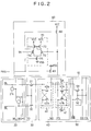
- FIG. 2 An example of such a dynamic RAM is shown in Fig. 2.
- Fig. 2 is a circuit diagram of the pertinent portion of the conventional semiconductor memory device.
- the semiconductor memory device is a dynamic RAM, comprising a memory cell array section 10, and a power source supply control section 60 for supplying a drive voltage to the memory cell array 10.
- the memory cell array section 10 comprises a data storage memory cell section 20, a transfer gate section 30 for transferring data of the memory cell section 20, a sense amplifier section 40 for sensing and amplifying a minute read voltage from the memory cell section 20, and a column decode section 60 for selecting the output of the sense amplifier section 40.
- a plurality of memory cells are disposed in a matrix arrangement, at intersections of a plurality of pairs of bit lines, such as BL, BL ⁇ , a plurality of word lines, such as WL i , WL i+1 .
- the memory cells 21 i , 21 i+1 and so on are formed of MOS transistors having a short gate length, so it is made to operate on an internal or auxiliary power source voltage V D (e.g., 3.3V) of a lower level than the main power source V CC (e.g., 5V).
- V D internal or auxiliary power source voltage
- V CC e.g., 5V
- the transfer gate section 30 is comprised of a plurality of pairs of n-channel MOS transistors (hereinafter referred to as NMOSTs) 31, 32 and so on, and which are turned on and off on the basis of a control signal TG to couple or isolate the pairs of bit lines BL, BL ⁇ , etc. and the pair of sense amplifier nodes SA, SA ⁇ , etc.
- the drains of the NMOSTs 31 and 32 are connected to the bit lines BL, BL ⁇ , and their sources are connected to the sense amplifier nodes SA, SA ⁇ , and their gates are commonly connected to receive the control signal TG.
- the sense amplifier section 40 is comprised of a plurality of p-channel sense amplifiers 41 and so on, and n-channel sense amplifiers 42 and so on, connected to the respective pairs of bit lines BL, BL ⁇ .
- the p-channel sense amplifiers 41 are comprised of two p-channel MOS transistors (hereinafter referred to as PMOSTs) 41a and 41b.
- the PMOST 41a has its drain connected to the sense amplifier node SA, its source connected to sense amplifier drive common node PS, and its gate connected to the sense amplifier node SA ⁇ .
- the PMOST 41b has its drain connected to the sense amplifier node SA ⁇ , its source connected to the common node PS, and its gate connected to the sense amplifier node SA.
- the n-channel sense amplifiers 42 are comprised of two n-channel MOSTs 42a and 42b.
- the NMOST 42a has its drain connected to the sense amplifier node SA, its source connected to sense amplifier drive common node NS, and its gate connected to the sense amplifier node SA ⁇ .
- the PMOST 42b has its drain connected to the sense amplifier node SA ⁇ , its source connected to the common node NS, and its gate connected to the sense amplifier node SA.
- the column decode section 50 comprises a plurality of pairs of NMOSTs 51, 52 for connecting and disconnecting the pairs of the sense amplifier nodes SA, SA ⁇ and so on, and the pairs of data lines DB, DB ⁇ and so on, and their gates are controlled by the column decoder output signal CL.
- the power source supply control section 60 comprises a current mirror amplifier 70 serving as a comparing and amplifying means, and PMOST 80 and NMOST 81 serving as a power source supply means.
- the current mirror amplifler 70 is activated by a control signal PAS, and compares and amplifies the voltage on the p-channel sense amplifier drive common node PS and a reference voltage V R of the same level as the auxiliary power source voltage V D . It is comprised of two PMOSTs 71 and 72, and three NMOST 73, 74 and 75.
- the PMOST 80 serving as the power supply means has its drain and source respectively connected to the main power source voltage V CC and the common node PS, and its gate connected to the output of the amplifier 70.
- the NMOST 81 has its drain and source connected to the ground potential V SS and the n-channel sense amplifier drive common node NS, and its gate connected to receive the control signal PAS.
- the read operation in which the memory cell 21 i is selected is as follows:
- the word line WL i is raised to the High level, V D +Vt+ ⁇ (Vt: threshold voltage of NMOST; and ⁇ : a certain predetermined margin), and data is read from the memory cell 21 i to the bit line BL.
- the common node PS reaches the V D level and the output of the amplifier 70 rises to the High level, and the PMOST 80 is turned off, and supply of electric charge from the main power source voltage V CC to the p-channel sense amplifier 41 is terminated.
- RC value parasitic capacitance
- the column decoder output signal CL is raised, and the NMOST 51 and 52 are turned on, and the read data is transferred to the pair of data lines DB, DB ⁇ .
- the control signal TG is raised to the level of V D +Vt+ ⁇ .
- the potential on the bit lines BL, BL ⁇ become equal to the potentials on the sense amplifier nodes SA, SA ⁇ .
- the data on the senseamplifier nodes SA and SA ⁇ are thereby rewritten in the memory cell 21 i .
- the word line is thereafter lowered.
- the device of the above-described configuration had the following drawbacks.
- An object of the present invention is to provide a semiconductor memory device in which the power consumption at the current mirror amplifier is reduced, and the time for completing the charging of the bit line is shortened.
- the invention provides a semiconductor memory device comprising: a main or first primary power source providing a first power source voltage (V CC ); an auxiliary or second power source providing a second power source voltage (V D ) lower than said first power source voltage (V CC ); a plurality of memory cells (21 i , 21 i+1 ) disposed at intersections of a plurality of bit lines (BL, BL ⁇ ) and a plurality of word lines (WL i , WL i+1 ) and operating on the second power source voltage (V D ); a plurality of sense amplifiers (41) activated by a voltage on a drive common node (NS) and sensing and amplifying the voltage on a corresponding one of the bit line; a comparing means (110) activated by said control signal (PAS) and comparing the voltage on the common node (PS) and said second power source voltage (V D ), the comparing means having an output which is in a first state when the voltage on the common node
- the latch means when the control signal rises to the High level, the latch means is turned from the first state to the second state, and the comparing means and the first power source supply means are thereby activated.
- the first power source supply means then supplies the drive voltage from the power source to the common node, to activate the sense amplifier.
- the sense amplifier then senses and amplifies the minute potential on the bit line.
- the potential on the common node is compared with the reference voltage by the comparing means, and when the potential on the common node is raised to the level of the second power source voltage, for example, and the latching means is returned from the second state to the first state. Then, the operation of the comparing means is terminated.
- the period for which the comparing means is activated is therefore shortened, and the power consumption is reduced.
- the semiconductor memory device may further be provided with a second power source supply means (131, 133) supplying the drive voltage to said common node (PS) in accordance with said control signal (PAS).
- a second power source supply means 131, 133 supplying the drive voltage to said common node (PS) in accordance with said control signal (PAS).
- the second power source supply means When the control signal goes High, the second power source supply means is activated to supply the drive voltage to the common node.
- the drive voltage is supplied continuously via the common node to the sense amplifier, so the time taken to complete the charging, for example, of the bit line is shortened, and the operation speed is further increased.
- the semiconductor memory may further be provided with a monitor means (150) receiving the voltage on the common node (PS) and detecting the voltage level on the bit line and applying the result of the detection to the comparing means (110).
- a monitor means 150 receiving the voltage on the common node (PS) and detecting the voltage level on the bit line and applying the result of the detection to the comparing means (110).
- the power source supply means supplies the drive voltage to the common node
- the potential on the common node is input to the monitor means.
- the monitor means monitors, on the basis of the voltage on the common node, the voltage level on the bit line.
- the result of monitoring lags behind the voltage rise, for example, on the common node.
- the lagging result of monitoring is compared with the reference voltage at the comparing means, so the operation for returning the latching means to the first state responsive to the output of the comparing means lags, and, as a result, the first power source supply means continues supplying the drive voltage for a longer period, and raises the common node above the second power source voltage.
- the charging and discharging of the of the bit line by the sense amplifier are made at a higher speed.
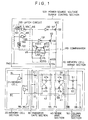
- Fig. 1 is a circuit diagram showing the pertinent portion of a semiconductor memory device of a first embodiment of the invention.
- Fig. 2 is a circuit diagram showing the pertinent portion of the semiconductor memory device in the prior art.
- Fig. 3 is a waveform diagram showing the operation of the circuit of Fig. 2.
- Fig. 4 is a circuit diagram showing a one-shot pulse generating circuit in Fig. 1.
- Fig. 5 is a waveform diagram showing the operation of the circuit of Fig. 1.
- Fig. 6 is a circuit diagram showing the pertinent portion of a second embodiment of the invention.
- Fig. 7 is a waveform diagram showing the operation of the circuit of Fig. 6.
- Fig. 1 is a circuit diagram of the pertinent portion of the semiconductor memory device of an embodiment of the invention. Elements common with the elements in the prior art of Fig. 2 are given identical reference marks.
- the semiconductor memory device is a dynamic RAM, and comprises a memory cell array section 10 identical to that of the prior art, and a power source voltage supply control section 100 which differs from that of the prior art.
- the power source voltage supply control section 100 supplies a drive voltage to the memory cell array 10, and is comprised of a comparator 110, which also has the function of amplification, a latch circuit 120, serving as a latching means, inverters 130 and 131 for inverting the signal, a PMOST 132 and an NMOST 134 serving as a main power source supply means, and a PMOST 133 serving as an auxiliary power source supply means.
- the NMOST 134 serves also as part of the auxiliary power source supply means.
- the comparator 110 is in the form of a current mirror amplifier which compares and amplifies the reference voltage V R (the same level as the auxiliary voltage V D ⁇ V CC ) and the voltage on the p-channel sense amplifier drive common node PS, and is comprised of PMOSTs 111 and 112, and NMOSTs 113, 114 and 115 connected as illustrated.
- the sources of the PMOSTs 111 and 112 are connected to the power source voltage V CC , and their gates are commonly connected to the drain node N1 of the PMOST 112.
- the source node N1 of the PMOST 112 is connected via the NMOST 113 to a node N3, and the gate of the NMOST 113 is connected to the common node PS.
- the drain node of the PMOST 113 is connected via the NMOST 114 to the node N3.
- the gate of the NMOST 114 is connected to the reference voltage V R .
- the node N3 is connected via the NMOST 115 to the ground potential V SS .
- the node N2 is connected to the latch circuit 120.
- the latch circuit 120 latches the rise of the High level, for example, of the control signal PAS.
- the latch circuit 120 can assume either of a first state and a second state, and is turned from the first state to the second state when the control signal PAS rises from the Low level to the High level, and is turned from the first state to the second state when the output of the comparator 110 at the node N2 rises.
- the latch circuit 120 is in the second state, its output, at a node N6, is High to activate the comparator 110 and turns on the PMOST 132.
- the latch circuit 120 is in the first state, its output, at the node N6, is Low to deactivate the comparator 110 and turn off the PMOST 132.
- the latch circuit 120 is comprised of one-shot pulse generator circuits 121 and 122, and NAND gates 124 and 125.
- the control signal PAS is connected via the one-shot pulse generator circuit 121 to the node N4, which is connected to one input of the NAND gate 124.
- the output of the NAND gate 124 is connected to the node N6, which is connected to one input of the NAND gate 125.
- the control signal PAS is connected to another input of the NAND gate 125.
- a third input of the NAND gate 125 is connected to a node N8, which is connected to the output of the one-shot pulse generator circuit 122, of which the input is connected to the node N2, later described.
- the output of the NAND gate 125 is connected to a node N5, which is connected to a second input of the NAND gate 124. In this way, the NAND gates 124 and 125 are crossed coupled.
- the node N6 is connected via the inverter 130 and the node N7 to the gate of the PMOST 132, and the source of the PMOST 132 is connected to the power source voltage V CC , and its drain is connected to the p-channel sense amplifier drive common node PS.
- the control signal PAS is connected via the inverter 131 to the gate of the PMOST 133, and the source of the PMOST 133 is connected to the auxiliary power source voltage V D , and its drain is connected to the common node PS.
- the control signal PAS is connected to the gate of the NMOST 134, and the source of the NMOST 134 is connected to the ground potential V SS , and its drain is connected to the n-channel sense amplifier drive common node NS.
- Fig. 4 is a circuit diagram showing an example of the one-shot pulse generator circuit 121 or 122 in Fig. 1.
- the one-shot pulse generator circuit 121 or 122 is a circuit for generating an inverted single pulse at the rising edge of the input signal, and is comprised of a cascaded inverters 140 to 142, and capacitors 143 to 145 connected between the outputs of the inverters 140 to 142 and the ground potential V SS , and a NAND gate 146 performing a logical NAND operation on the input signal and the output signal of the inverter 142.
- the word line WL i is raised to the High level, V D +Vt+ ⁇ (Vt: threshold voltage of NMOST; and ⁇ : a certain predetermined margin), and data is read from the memory cell 21 i to the bit line BL.
- the latch circuit 120 is turned from the first state to the second state responsive to the rise of the control signal PAS and is held in the second state.
- the rise of the node N6 is transferred through the inverter 130 and the node N7, and the PMOST 132 is turned on, and the NMOST 115 is turned on, and the comparator 110 is activated.
- the NMOST 115 As the NMOST 115 is turned on a current flows through the node N2, the NMOST 114, the node N3, and the NMOST 115 and to the ground V SS . As a result, the potential on the node N2 falls a little.
- the NMOST 134 As the NMOST 134 is turned on, the n-channel sense amplifier drive common node NS is pulled down to the ground level V SS . Furthermore, as the PMOST 132 is turned on, the p-channel sense amplifier drive node PS is raised toward the auxiliary power source voltage V D level. Then, the p-channel sense amplifier 41 and the n-channel sense amplifier 42 are activated, and because of their sensing and amplifying operation, one of the sense amplifier nodes, e.g., SA ⁇ , and one of the bit line, e.g., BL ⁇ , which are higher are charged and those which are lower, e.g., SA and BL, are discharged.
- SA ⁇ sense amplifier nodes
- the bit line e.g., BL ⁇
- the node N2 will be at the power source voltage V CC level. That is, when the common node PS reaches the V D level, the node N1 falls from the V CC level to the V SS level, and as a result, the output node N2 returns to the V CC level. Then, an inverted one-shot pules is generated on the output node N8 of the one-shot pulse generator circuit 122 in the latch circuit 120 generates, and this one-shot pulse is input to the NAND gate 125, with the result that the output node N6 of the NAND gate 124 falls from the High level to the Low level. In other words, the latch circuit 120 is returned from the second state to the first state.
- the fall of the node N6 is transferred via the inverter 130, and the PMOST 132 is turned off, and the supply of the electric charge from the power source voltage V CC to the p-channel sense amplifier 41 is terminated, and the NMOST 115 is turned off and the comparator 110 is deactivated. After this, the supply of the electric charge to the p-channel sense amplifier 42 is made only from the auxiliary power source voltage V D via the PMOST 133.
- the column decoder output signal CL is raised to the High level to turn on the NMOSTs 51 and 52, thereby to transfer the data from the pair of sense amplifier nodes SA and SA ⁇ to the pair of data lines DB and DB ⁇ .
- the control signal TG is raised from the V D level to the V D +Vt+ ⁇ level, and the potentials on the bit lines BL and BL ⁇ are made equal to the potentials on the sense amplifier nodes SA and SA ⁇ .
- the potentials on the sense amplifier nodes SA and SA ⁇ are thereby written via the bit lines into the memory cell 21 i .
- Fig. 6 is a circuit diagram showing the pertinent portion of the semiconductor memory device of a second embodiment of the invention. Elements identical to those in Fig. 1 are given identical or common reference marks.
- the power source voltage supply control section 100A of this semiconductor memory device differs from that of Fig. 1 in that, in place of the PMOST 133 and the inverter 131, a monitor circuit 150 serving as a monitor means is provided. In other respects, the configuration is identical to the power source voltage supply control section 100 of Fig. 1.
- the monitor circuit 150 is disposed between the p-channel sense amplifier drive common node PS and the input node N9 of the comparator 110, and has the functions of monitoring the voltage level of the higher one of the bit lines BL and BL ⁇ , and applying the result of the monitoring to the input node N9.
- the monitor circuit 150 comprises a NMOST 51 having the same characteristics as the NMOSTs 31 and 32 in the transfer gate section 30, and a bit line capacitor 152 formed of a MOS capacitor or the like.
- the drain and the source of the NMOST 151 are connected to the common node PS and the input node N9 of the comparator 110, and the gate of the NMOST 151 is connected to receive the control signal TG.
- the input node N9 is connected via the bit line capacitor 152 to the ground potential V SS .
- the word line WL i is raised to the High level, V D +Vt+ ⁇ , and as in the waveform of Fig. 5, the potential on the bit line BL and the sense amplifier node SA varies by the amount of the read signal from the precharge level (e.g., V D /2).
- the NMOST 134 is turned on, and the n-channel sense amplifier drive common node NS falls to V SS level.
- the rise of the output node N6 of the latch circuit 120 turns on the PMOST 132, and turns on the NMOST 115, to activate the comparator 110.
- the PMOST 132 is turned on, the p-channel sense amplifier drive common node PS is raised to V D by virtue of the main power source voltage V CC .
- the common node PS rises beyond the V D level toward the V CC level.
- the common node PS thereby exceeds the V D level, and, by the action of the monitor circuit 150, the input node N9 of the comparator 110 rises to the same level as the higher one of the bit lines, e.g., BL ⁇ , and until then, the output node N2 of the comparator 110 is kept lower than the V CC level.
- the latch circuit 120 continues to be in the second state, and its output node N6 is kept High, so the PMOST 132 is kept on, and the supply of electric charge to the p-channel sense amplifier 41 is continued. Accordingly, charging and discharging of the sense amplifier nodes SA and SA ⁇ and the bit lines BL and BL ⁇ are accomplished at a high speed.
- the decoder output signal CL rises, and the data is transferred to the pair of data lines DB and DB ⁇ .
- the control signal TG is raised to V D +Vt+ ⁇ .
- the level of the higher one of the bit lines rises again.
- the common node PS and the higher one of the sense amplifier nodes, e.g., SA ⁇ have been charged above the V D level
- the higher bit line BL ⁇ rapidly rises, and reaches the V D level at time t3.
- the input node N9 of the comparator 110 reaches the V D level, and, at this instance, the output node N2 of the comparator 110 returns to the V CC level, and the latch circuit 20 is returned from the second state to the first state, and the output node N6 falls to the Low level.
- a latch means is provided, so by the action of the latch means, the comparing and amplifying means is deactivated immediately upon completion of the bit line charging, and the current consumed at the comparing and amplifying means is reduced, and the power consumption is thereby reduced.
- An auxiliary power source supply means may additionally be provided.
- the auxiliary power source supply means continues the supply of the electric charge from the power source to the sense amplifier until the potential on the bit line reaches a predetermined level, so the charging of the bit line is accomplished with a high speed, and the high speed operation is thereby enabled.
- the return of the latch circuit from the second state to the first state responsive to the output of the comparing and amplifying means is retarded, and by means of the output of the latch means, the main power source supply means is kept on. Accordingly, the electric charge is kept supplied from the main power source to the sense amplifier until the potential on the bit line reaches a predetermined level, so the charging of the bit line is accomplished with a high speed, and the high-speed operation is possible.
Abstract
Description
- The present invention relates to a semiconductor memory device such as a dynamic RAM (random access memory) or a static RAM, and more particularly to a method of controlling supply of power to the memory cell array.
- A conventional technique in this field is disclosed in Technical Paper of the Institute of Electronics, Information and Communication Engineers of Japan, 89n[67] (1989-6-2), Koike, et al "55ns 16Mb DRAM with Built-in-Self-Test Function Using Micro-Program ROM", pp. 79-80.
- As described in this publication, the cell size of a semiconductor memory device, e.g., a dynamic RAM of a large capacity, is small, so the breakdown voltage of the transistor forming the cell array is low. To improve the reliabillty, the power source voltage VCC (e.g., 5V) needs to be lowered. Accordingly, use is made of a power source supply control section which produces, from the externally-supplied power source voltage (primary or main power source voltage) VCC an internal (secondary or auxiliary) power source voltage VD (e.g., 3.3V), which is then used for driving the memory cell array. An example of such a dynamic RAM is shown in Fig. 2.
- Fig. 2 is a circuit diagram of the pertinent portion of the conventional semiconductor memory device.
- The semiconductor memory device is a dynamic RAM, comprising a memory
cell array section 10, and a power sourcesupply control section 60 for supplying a drive voltage to thememory cell array 10. - The memory
cell array section 10 comprises a data storagememory cell section 20, atransfer gate section 30 for transferring data of thememory cell section 20, asense amplifier section 40 for sensing and amplifying a minute read voltage from thememory cell section 20, and acolumn decode section 60 for selecting the output of thesense amplifier section 40. - In the
memory cell section 20, a plurality of memory cells (only two of them, 21i, 21i+1, being illustrated) are disposed in a matrix arrangement, at intersections of a plurality of pairs of bit lines, such as BL,
- The
transfer gate section 30 is comprised of a plurality of pairs of n-channel MOS transistors (hereinafter referred to as NMOSTs) 31, 32 and so on, and which are turned on and off on the basis of a control signal TG to couple or isolate the pairs of bit lines BL,

NMOSTs 

- The
sense amplifier section 40 is comprised of a plurality of p-channel sense amplifiers 41 and so on, and n-channel sense amplifiers 42 and so on, connected to the respective pairs of bit lines BL,
- For instance, the p-
channel sense amplifiers 41 are comprised of two p-channel MOS transistors (hereinafter referred to as PMOSTs) 41a and 41b. The PMOST 41a has its drain connected to the sense amplifier node SA, its source connected to sense amplifier drive common node PS, and its gate connected to the sense amplifier node

- The n-
channel sense amplifiers 42 are comprised of two n-channel MOSTs 

- The
column decode section 50 comprises a plurality of pairs ofNMOSTs 

- The power source
supply control section 60 comprises acurrent mirror amplifier 70 serving as a comparing and amplifying means, and PMOST 80 and NMOST 81 serving as a power source supply means. - The
current mirror amplifler 70 is activated by a control signal PAS, and compares and amplifies the voltage on the p-channel sense amplifier drive common node PS and a reference voltage VR of the same level as the auxiliary power source voltage VD. It is comprised of two PMOSTs 71 and 72, and threeNMOST amplifier 70. The NMOST 81 has its drain and source connected to the ground potential VSS and the n-channel sense amplifier drive common node NS, and its gate connected to receive the control signal PAS. - The operation of the circuit shown in Fig. 2 is described with reference to Fig. 3.
- The read operation in which the memory cell 21i is selected is as follows:
- First, at time t0, the word line WLi is raised to the High level, VD+Vt+α (Vt: threshold voltage of NMOST; and α : a certain predetermined margin), and data is read from the memory cell 21i to the bit line BL. As a result, the potential on the bit line BL and the sense amplifier node SA varies by the amount of the read signal from the precharge level (e.g., VD/2).
- At time t1, the control signal PAS is raised to the High level (=VCC), and the
NMOST 81 is turned on, and the n-channel sense amplifier drive common node NS varies to the Low level (=VSS). At the same time, the NMOST 75 is turned on, and theamplifier 70 is activated, and by virtue of the Low level output of theamplifier 70, the PMOST 80 is turned on, and the p-channel sense amplifier drive common node PS is pulled up to the High level (=VD). As a result, by the sensing and amplifying action of the p-channel sense amplifier 41 and the n-channel sense amplifier 42, charging and discharging of the pair of the sense amplifier nodes SA,

- At time t2, the common node PS reaches the VD level and the output of the
amplifier 70 rises to the High level, and the PMOST 80 is turned off, and supply of electric charge from the main power source voltage VCC to the p-channel sense amplifier 41 is terminated. - The parasitic capacitance (=RC value) of the pair of bit lines BL,


channel sense amplifier 41 is intermittently supplied. - At time t3, after the potential difference between the pair of sense amplifier nodes SA,

NMOST 


- The device of the above-described configuration had the following drawbacks.
- (i) In the conventional device, the control signal PAS is raised to the High level at time t1, to activate the
current mirror amplifier 70, so that theamplifier 70 is kept activated. The power consumption at theamplifier 70 is therefore large. - (ii) The PMOST 80 is repetitively turned on and off during time t2 to t4, and electric charge is repetitively supplied from the main power source VCC to the p-
channel sense amplifier 41 so time required for completing charging of the bit line BL or
- An object of the present invention is to provide a semiconductor memory device in which the power consumption at the current mirror amplifier is reduced, and the time for completing the charging of the bit line is shortened.
- To solve the problems described above, the invention provides a semiconductor memory device comprising:
a main or first primary power source providing a first power source voltage (VCC);
an auxiliary or second power source providing a second power source voltage (VD) lower than said first power source voltage (VCC);
a plurality of memory cells (21i, 21i+1) disposed at intersections of a plurality of bit lines (BL,
a plurality of sense amplifiers (41) activated by a voltage on a drive common node (NS) and sensing and amplifying the voltage on a corresponding one of the bit line;
a comparing means (110) activated by said control signal (PAS) and comparing the voltage on the common node (PS) and said second power source voltage (VD), the comparing means having an output which is in a first state when the voltage on the common node (PS) is not higher than the reference voltage (VR) and which is in a second state when the voltage on the common node (PS) exceeds the reference voltage (VR); and
a first power source supply means (130, 132) controlled in accordance with the output of said comparing means (110) and supplying a drive voltage to said common node (PS) when said control signal (PAS) is active;
characterized by further comprising:
a latch means (120) selectively assuming a first state and a second state, receiving the control signal (PAS) and the output of said comparing means (110), turned from the first state to the second state when the control signal (PAS) is turned active, thereby to activate the comparing means (110) and the first power source supply means (130, 132), and turned from the second state to the first state when the output of said comparing means (110) is turned to from the first state to the said second state, said latching means deactivating the comparing means (110) when it is turned to the first state. - In the semiconductor memory device configured as described above, when the control signal rises to the High level, the latch means is turned from the first state to the second state, and the comparing means and the first power source supply means are thereby activated. The first power source supply means then supplies the drive voltage from the power source to the common node, to activate the sense amplifier. The sense amplifier then senses and amplifies the minute potential on the bit line. The potential on the common node is compared with the reference voltage by the comparing means, and when the potential on the common node is raised to the level of the second power source voltage, for example, and the latching means is returned from the second state to the first state. Then, the operation of the comparing means is terminated. The period for which the comparing means is activated is therefore shortened, and the power consumption is reduced.
- The semiconductor memory device may further be provided with a second power source supply means (131, 133) supplying the drive voltage to said common node (PS) in accordance with said control signal (PAS).
- When the control signal goes High, the second power source supply means is activated to supply the drive voltage to the common node. The drive voltage is supplied continuously via the common node to the sense amplifier, so the time taken to complete the charging, for example, of the bit line is shortened, and the operation speed is further increased.
- The semiconductor memory may further be provided with a monitor means (150) receiving the voltage on the common node (PS) and detecting the voltage level on the bit line and applying the result of the detection to the comparing means (110).
- When the power source supply means supplies the drive voltage to the common node, the potential on the common node is input to the monitor means. The monitor means monitors, on the basis of the voltage on the common node, the voltage level on the bit line. The result of monitoring lags behind the voltage rise, for example, on the common node. The lagging result of monitoring is compared with the reference voltage at the comparing means, so the operation for returning the latching means to the first state responsive to the output of the comparing means lags, and, as a result, the first power source supply means continues supplying the drive voltage for a longer period, and raises the common node above the second power source voltage. As a result, the charging and discharging of the of the bit line by the sense amplifier are made at a higher speed.
- Fig. 1 is a circuit diagram showing the pertinent portion of a semiconductor memory device of a first embodiment of the invention.
- Fig. 2 is a circuit diagram showing the pertinent portion of the semiconductor memory device in the prior art.
- Fig. 3 is a waveform diagram showing the operation of the circuit of Fig. 2.
- Fig. 4 is a circuit diagram showing a one-shot pulse generating circuit in Fig. 1.
- Fig. 5 is a waveform diagram showing the operation of the circuit of Fig. 1.
- Fig. 6 is a circuit diagram showing the pertinent portion of a second embodiment of the invention.
- Fig. 7 is a waveform diagram showing the operation of the circuit of Fig. 6.
- Fig. 1 is a circuit diagram of the pertinent portion of the semiconductor memory device of an embodiment of the invention. Elements common with the elements in the prior art of Fig. 2 are given identical reference marks.
- The semiconductor memory device is a dynamic RAM, and comprises a memory
cell array section 10 identical to that of the prior art, and a power source voltagesupply control section 100 which differs from that of the prior art. - The power source voltage
supply control section 100 supplies a drive voltage to thememory cell array 10, and is comprised of acomparator 110, which also has the function of amplification, alatch circuit 120, serving as a latching means,inverters NMOST 134 serving as a main power source supply means, and aPMOST 133 serving as an auxiliary power source supply means. TheNMOST 134 serves also as part of the auxiliary power source supply means. - The
comparator 110 is in the form of a current mirror amplifier which compares and amplifies the reference voltage VR (the same level as the auxiliary voltage VD<VCC) and the voltage on the p-channel sense amplifier drive common node PS, and is comprised ofPMOSTs NMOSTs - The sources of the
PMOSTs PMOST 112. The source node N1 of thePMOST 112 is connected via theNMOST 113 to a node N3, and the gate of theNMOST 113 is connected to the common node PS. The drain node of thePMOST 113 is connected via theNMOST 114 to the node N3. The gate of theNMOST 114 is connected to the reference voltage VR. The node N3 is connected via theNMOST 115 to the ground potential VSS. The node N2 is connected to thelatch circuit 120. - The
latch circuit 120 latches the rise of the High level, for example, of the control signal PAS. In other words, thelatch circuit 120 can assume either of a first state and a second state, and is turned from the first state to the second state when the control signal PAS rises from the Low level to the High level, and is turned from the first state to the second state when the output of thecomparator 110 at the node N2 rises. When thelatch circuit 120 is in the second state, its output, at a node N6, is High to activate thecomparator 110 and turns on the PMOST 132. When thelatch circuit 120 is in the first state, its output, at the node N6, is Low to deactivate thecomparator 110 and turn off the PMOST 132. - The
latch circuit 120 is comprised of one-shotpulse generator circuits NAND gates pulse generator circuit 121 to the node N4, which is connected to one input of theNAND gate 124. The output of theNAND gate 124 is connected to the node N6, which is connected to one input of theNAND gate 125. The control signal PAS is connected to another input of theNAND gate 125. A third input of theNAND gate 125 is connected to a node N8, which is connected to the output of the one-shotpulse generator circuit 122, of which the input is connected to the node N2, later described. The output of theNAND gate 125 is connected to a node N5, which is connected to a second input of theNAND gate 124. In this way, theNAND gates - The node N6 is connected via the
inverter 130 and the node N7 to the gate of the PMOST 132, and the source of the PMOST 132 is connected to the power source voltage VCC, and its drain is connected to the p-channel sense amplifier drive common node PS. The control signal PAS is connected via theinverter 131 to the gate of thePMOST 133, and the source of thePMOST 133 is connected to the auxiliary power source voltage VD, and its drain is connected to the common node PS. The control signal PAS is connected to the gate of theNMOST 134, and the source of theNMOST 134 is connected to the ground potential VSS, and its drain is connected to the n-channel sense amplifier drive common node NS. - Fig. 4 is a circuit diagram showing an example of the one-shot
pulse generator circuit - The one-shot
pulse generator circuit inverters 140 to 142, and capacitors 143 to 145 connected between the outputs of theinverters 140 to 142 and the ground potential VSS, and aNAND gate 146 performing a logical NAND operation on the input signal and the output signal of theinverter 142. - The operation of the circuit shown in Fig. 1 will now be described with reference to Fig. 5.
- The reading operation in the case when the memory cell 21i in Fig. 1 is selected will now be described.
- At time t0, the word line WLi is raised to the High level, VD+Vt+α (Vt: threshold voltage of NMOST; and α : a certain predetermined margin), and data is read from the memory cell 21i to the bit line BL. As a result, the potential on the bit line BL and the sense amplifier node SA varies by the amount of the read signal from the precharge level (VD/2).
- At time t1, the control signal PAS is raised to the High level (=VCC), then the
NMOST 134 is turned on and thePMOST 133 is turned on via theinverter 131. Furthermore, responsive to the rise of the control signal PAS, an inverted one-shot pulse is output from the one-shotpulse generator circuit 121 to the node N4. The fall of the node N4 is transferred through theNAND gates NAND gate 124 rises, and the output node N5 of theNAND gate 125 falls. The crossed-coupledNAND gates latch circuit 120 is turned from the first state to the second state responsive to the rise of the control signal PAS and is held in the second state. The rise of the node N6 is transferred through theinverter 130 and the node N7, and the PMOST 132 is turned on, and theNMOST 115 is turned on, and thecomparator 110 is activated. - As the
NMOST 115 is turned on a current flows through the node N2, theNMOST 114, the node N3, and theNMOST 115 and to the ground VSS. As a result, the potential on the node N2 falls a little. - As the
NMOST 134 is turned on, the n-channel sense amplifier drive common node NS is pulled down to the ground level VSS. Furthermore, as the PMOST 132 is turned on, the p-channel sense amplifier drive node PS is raised toward the auxiliary power source voltage VD level. Then, the p-channel sense amplifier 41 and the n-channel sense amplifier 42 are activated, and because of their sensing and amplifying operation, one of the sense amplifier nodes, e.g.,

- At time t2, when the p-channel sense amplifier drive common node PS reaches the VD level, the node N2 will be at the power source voltage VCC level. That is, when the common node PS reaches the VD level, the node N1 falls from the VCC level to the VSS level, and as a result, the output node N2 returns to the VCC level. Then, an inverted one-shot pules is generated on the output node N8 of the one-shot
pulse generator circuit 122 in thelatch circuit 120 generates, and this one-shot pulse is input to theNAND gate 125, with the result that the output node N6 of theNAND gate 124 falls from the High level to the Low level. In other words, thelatch circuit 120 is returned from the second state to the first state. - The fall of the node N6 is transferred via the
inverter 130, and the PMOST 132 is turned off, and the supply of the electric charge from the power source voltage VCC to the p-channel sense amplifier 41 is terminated, and theNMOST 115 is turned off and thecomparator 110 is deactivated. After this, the supply of the electric charge to the p-channel sense amplifier 42 is made only from the auxiliary power source voltage VD via thePMOST 133. - When an adequate potential difference is created between the pair of sense amplifier nodes SA and

NMOSTs 


- This first embodiment has the following advantages:
- (a) Since the
latch circuit 120 is provided, responsive to the rise of the control signal PAS, the output node N6 of thelatch circuit 120 is raised to the High level and the PMOST 132 is turned on, and the supply of electric charge to the p-channel sense amplifier 41 is conducted, and thecomparator 110 is activated. When the common node PS rises to the VD level, the output node N2 of thecomparator 110 becomes the VCC level, and the output node N6 of thelatch circuit 120 becomes the Low level, and thecomparator 110 is deactivated. Accordingly, the time for which thecomparator 110 is activated is minimized, and the current through thecomparator 110 is reduced, and the power consumption is reduced. - (b) The
PMOST 133 is provided as an auxiliary power source supply means, and is on for the period for which the control signal PAS is at the High level, and the electric charge is supplied from the auxiliary power source voltage VD to the p-channel sense amplifier 41. Accordingly, after the PMOST 132 has been turned off, thePMOST 133 keeps supplying the electric charge to the p-channel sense ampllfier 41, and the time for charging the bit line BL or
- Fig. 6 is a circuit diagram showing the pertinent portion of the semiconductor memory device of a second embodiment of the invention. Elements identical to those in Fig. 1 are given identical or common reference marks.
- The power source voltage
supply control section 100A of this semiconductor memory device differs from that of Fig. 1 in that, in place of thePMOST 133 and theinverter 131, amonitor circuit 150 serving as a monitor means is provided. In other respects, the configuration is identical to the power source voltagesupply control section 100 of Fig. 1. - The
monitor circuit 150 is disposed between the p-channel sense amplifier drive common node PS and the input node N9 of thecomparator 110, and has the functions of monitoring the voltage level of the higher one of the bit lines BL and
- The
monitor circuit 150 comprises a NMOST 51 having the same characteristics as theNMOSTs transfer gate section 30, and abit line capacitor 152 formed of a MOS capacitor or the like. The drain and the source of theNMOST 151 are connected to the common node PS and the input node N9 of thecomparator 110, and the gate of theNMOST 151 is connected to receive the control signal TG. The input node N9 is connected via thebit line capacitor 152 to the ground potential VSS. - The operation of the circuit shown in Fig. 6 will now be described with reference to Fig. 7.
- For example, let us assume that the memory cell 21i is selected for reading, as in the description of the operation of the circuit of Fig. 1.
- At time t0, the word line WLi is raised to the High level, VD+Vt+α , and as in the waveform of Fig. 5, the potential on the bit line BL and the sense amplifier node SA varies by the amount of the read signal from the precharge level (e.g., VD/2).
- At time t1, the control signal PAS is raised to the High level (=VCC). Then, the
NMOST 134 is turned on, and the n-channel sense amplifier drive common node NS falls to VSS level. At the same time, as in Fig. 5, the rise of the output node N6 of thelatch circuit 120 turns on the PMOST 132, and turns on theNMOST 115, to activate thecomparator 110. When the PMOST 132 is turned on, the p-channel sense amplifier drive common node PS is raised to VD by virtue of the main power source voltage VCC. - By the sensing and amplifying action of the
sense amplifiers 


- While the PMOST 132 is on, the common node PS rises beyond the VD level toward the VCC level. The common node PS thereby exceeds the VD level, and, by the action of the
monitor circuit 150, the input node N9 of thecomparator 110 rises to the same level as the higher one of the bit lines, e.g.,
comparator 110 is kept lower than the VCC level. For this reason, thelatch circuit 120 continues to be in the second state, and its output node N6 is kept High, so the PMOST 132 is kept on, and the supply of electric charge to the p-channel sense amplifier 41 is continued. Accordingly, charging and discharging of the sense amplifier nodes SA and

- After an adequate potential difference is created between the sense amplifier nodes SA and


- As a result, the level of the higher one of the bit lines, e.g.,


comparator 110 reaches the VD level, and, at this instance, the output node N2 of thecomparator 110 returns to the VCC level, and thelatch circuit 20 is returned from the second state to the first state, and the output node N6 falls to the Low level. This is transferred via theinverter 130 and the node N7, and the PMOST 132 is turned off, so the supply of electric charge to the p-channel sense amplifier 41 is terminated, and theNMOST 115 is turned off and thecomparator 110 is deactivated. - The advantages of the second embodiment are as follows:
- (a) Since the
monitor circuit 150 is provided, it is possible to supply the electric charge, with a voltage higher than in the first embodiment, to the p-channel sense amplifier 41 via the PMOST 132 which is kept on until the higher one of the bit line, e.g.,

- (b) At the same time as the completion of the charging of the bit line, e.g.,

latch circuit 120 is returned from the second state to the first state by the output of thecomparator 110, and thecomparator 110 is deactivated by the output of thelatch circuit 120, so the current consumed by thecomparator 110 is reduced and the reduction in power consumption is achieved. - The present invention is not limited to the illustrated embodiments. Examples of modifications are as follows:
- (i) The
comparator 110 may be formed of other transistors and the like, and may be replaced by a circuit of any different configuration or any other type of comparing means. - (ii) The
latch circuit 120 may be formed of latch means using other gate circuits such as NOR gates. - (iii) The main power source supply means and the auxiliary power source supply means may be formed of other types of transistors. The
monitor circuit 150 serving as an auxiliary power source supply means may be of a circuit configuration employing other transistors and the like. - (iv) The memory
cell array section 10 may be formed of a circuit other than that illustrated. The invention can be applied to semiconductor memory devices, such as static RAMs, other than dynamic RAMs. - As has been described, according to the invention, a latch means is provided, so by the action of the latch means, the comparing and amplifying means is deactivated immediately upon completion of the bit line charging, and the current consumed at the comparing and amplifying means is reduced, and the power consumption is thereby reduced.
- An auxiliary power source supply means may additionally be provided. In such a case, when the main power source supply means is off, the auxiliary power source supply means continues the supply of the electric charge from the power source to the sense amplifier until the potential on the bit line reaches a predetermined level, so the charging of the bit line is accomplished with a high speed, and the high speed operation is thereby enabled.
- In the embodiment of Fig. 6, in which a monitor means is provided, the return of the latch circuit from the second state to the first state responsive to the output of the comparing and amplifying means is retarded, and by means of the output of the latch means, the main power source supply means is kept on. Accordingly, the electric charge is kept supplied from the main power source to the sense amplifier until the potential on the bit line reaches a predetermined level, so the charging of the bit line is accomplished with a high speed, and the high-speed operation is possible.
Claims (16)
- A semiconductor memory device comprising:
a first power source providing a first power source voltage (VCC);
a second power source providing a second power source voltage (VD) lower than said first power source voltage (VCC);
a plurality of memory cells (21i, 21i+1) disposed at intersections of a plurality of bit lines (BL,
a plurality of sense amplifiers (41) activated by a voltage on a drive common node (NS) and sensing and amplifying the voltage on a corresponding one of the bit line;
a comparing means (110) activated by said control signal (PAS) and comparing the voltage on the common node (PS) and said second power source voltage (VD), the comparing means having an output which is in a first state when the voltage on the common node (PS) is not higher than the reference voltage (VR) and which is in a second state when the voltage on the common node (PS) exceeds the reference voltage (VR); and
a main power source supply means (130, 132) controlled in accordance with the output of said comparing means (110) and supplying a drive voltage to said common node (PS) when said control signal (PAS) is active;
characterized by further comprising:
a latch means (120) selectively assuming a first state and a second state, receiving the control signal (PAS) and the output of said comparing means (110), turned from the first state to the second state when the control signal (PAS) is turned active, thereby to activate the comparing means (110) and the main power source supply means (130, 132), and turned from the second state to the first state when the output of said comparing means (110) is turned to from the first state to the said second state, said latching means deactivating the comparing means (110) when it is turned to the first state. - The device of claim 1, further comprising a data line driven by said first power source, the data being transferred between said sensing amplifier and said data line.
- The device of claim 1, wherein said drive voltage supplied by said first power source supply means is said first power source voltage.
- The device of claim 1, wherein said main power source supply means supplies the drive voltage to the common node when the latch means is in said second state and it does not supplies the drive voltage to the common node when the latch means is in said first state.
- The device of claim 1, wherein said comparing means is a current mirror amplifier.
- The device of claim 1, wherein said control signal (PAS) is raised during reading at a time point when the data is to be read from the memory cell to the bit line.
- The device of claim 1, wherein said main power source supply means comprises a switch (132) coupling the common node with said first power source.
- The device of claim 1, characterized by further comprising:
a second power source supply means (131, 133) supplying the drive voltage to said common node (PS) in accordance with said control signal (PAS). - The device of claim 8, wherein said second power source supply means supplies the drive voltage to said common node when the control signal (PAS) is active.
- The device of claim 8, wherein the drive voltage supplied by said second power source supply means (131, 133) is said second power source voltage.
- The device of claim 8, wherein said second power source supply means comprises a switch (133) coupling the common node with said second power source supply.
- The device of claim 1, further comprising:
a monitor means (150) receiving the voltage on the common node (PS) and detecting the voltage level on the bit line and applying the result of the detection to the comparing means (110). - The the device of claim 12, wherein said monitor means comprises a switch (151) coupling the common node (PS) with the comparing means (110), and being controlled by another control signal (TG), a capacitor connected across the input of said comparing means and the ground, said another control signal (TG) is active when the bit line the the sense amplifier is to be coupled, whereby the potential on the common node (PS) being transferred to the input of said comparing means with a delay due to said capacitor.
- A circuit for supplying charge to a sense amplifier during a memory read operation, comprising:
a source of charge (132) switchable between an on state and an off state;
a source of a control signal (PAS); and
a comparing means (110), including means (115) to enable and inhibit operation thereof, for comparing the voltage at a node (PS, N9) supplied with charge by said source of charge (132),with a reference voltage (VR) and outputting a signal dependent on said comparison;
characterised by
latch means (120) for turning on the source of charge (132) and causing the comparing means (110) to be enabled in response to a predetermined change in the control signal (PAS), and for turning off the source of charge (132) and causing the comparing means (110) to be inhibited in response to a predetermined change in the signal output by the comparing means (110). - A circuit according to claim 14 including an auxiliary source of charge (133) operating to supply charge to said node (PS) when the control signal (PAS) is in a prdetermined state and the source of charge (132) is in its off state.
- A dynamic memory circuit including a circuit according to claim 14, a bit line (BL,


Applications Claiming Priority (2)
| Application Number | Priority Date | Filing Date | Title |
|---|---|---|---|
| JP2224771A JP3037377B2 (en) | 1990-08-27 | 1990-08-27 | Semiconductor storage device |
| JP224771/90 | 1990-08-27 |
Publications (3)
| Publication Number | Publication Date |
|---|---|
| EP0473360A2 true EP0473360A2 (en) | 1992-03-04 |
| EP0473360A3 EP0473360A3 (en) | 1993-02-03 |
| EP0473360B1 EP0473360B1 (en) | 1996-12-18 |
Family
ID=16818963
Family Applications (1)
| Application Number | Title | Priority Date | Filing Date |
|---|---|---|---|
| EP91307719A Expired - Lifetime EP0473360B1 (en) | 1990-08-27 | 1991-08-22 | Semiconductor memory device |
Country Status (5)
| Country | Link |
|---|---|
| US (1) | US5258950A (en) |
| EP (1) | EP0473360B1 (en) |
| JP (1) | JP3037377B2 (en) |
| KR (1) | KR100205555B1 (en) |
| DE (1) | DE69123666T2 (en) |
Cited By (6)
| Publication number | Priority date | Publication date | Assignee | Title |
|---|---|---|---|---|
| GB2258329A (en) * | 1991-07-31 | 1993-02-03 | Samsung Electronics Co Ltd | Sense amplifier control circuit of a semiconductor memory device |
| EP0563521A2 (en) * | 1992-03-30 | 1993-10-06 | United Memories, Inc. | Low power DRAM |
| EP0568015A2 (en) * | 1992-04-28 | 1993-11-03 | Nec Corporation | Dynamic random access memory device with intermediate voltage generator interrupting power supply in test operation |
| EP0933785A1 (en) * | 1993-03-17 | 1999-08-04 | Fujitsu Limited | Semiconductor device and power supply current detecting method |
| CN102034532A (en) * | 2009-10-02 | 2011-04-27 | 台湾积体电路制造股份有限公司 | System and method for digital retention voltage generation |
| KR101842959B1 (en) | 2010-12-01 | 2018-03-28 | 에이알엠 리미티드 | Retention voltage generation |
Families Citing this family (24)
| Publication number | Priority date | Publication date | Assignee | Title |
|---|---|---|---|---|
| KR930008886B1 (en) * | 1991-08-19 | 1993-09-16 | 삼성전자 주식회사 | Power supply circuit doing electrical programmable |
| JPH05234380A (en) * | 1992-02-21 | 1993-09-10 | Sharp Corp | Semiconductor memory device |
| JP3305010B2 (en) * | 1992-09-04 | 2002-07-22 | 沖電気工業株式会社 | Semiconductor storage device |
| JP2744738B2 (en) * | 1992-09-07 | 1998-04-28 | 三菱電機株式会社 | Semiconductor storage device |
| KR960000837B1 (en) * | 1992-12-02 | 1996-01-13 | 삼성전자주식회사 | Semiconductor memory device |
| US5754478A (en) | 1993-04-20 | 1998-05-19 | Micron Technology, Inc. | Fast, low power, write scheme for memory circuits using pulsed off isolation device |
| JP2725571B2 (en) * | 1993-10-06 | 1998-03-11 | 日本電気株式会社 | Nonvolatile semiconductor memory device |
| US5465060A (en) * | 1994-06-10 | 1995-11-07 | International Business Machines Corporation | Fast edge triggered self-resetting CMOS receiver with parallel L1/L2 (Master/Slave) latch |
| JP2658916B2 (en) * | 1994-11-04 | 1997-09-30 | 日本電気株式会社 | Power supply switching circuit for semiconductor device |
| JP3510362B2 (en) * | 1995-01-10 | 2004-03-29 | 株式会社ルネサステクノロジ | Semiconductor storage device |
| JP3846748B2 (en) * | 1996-07-17 | 2006-11-15 | 株式会社ルネサステクノロジ | Semiconductor memory device |
| KR100226491B1 (en) * | 1996-12-28 | 1999-10-15 | 김영환 | Device for pull-up/pull-down of bitline sense amplifier in semiconductor memory and method thereof |
| KR100425440B1 (en) * | 1997-06-17 | 2004-05-24 | 삼성전자주식회사 | Control circuit of internal supply voltage generator of semiconductor device |
| KR100304952B1 (en) * | 1998-06-05 | 2001-09-24 | 김영환 | Semiconductor memory device |
| CA2277717C (en) * | 1999-07-12 | 2006-12-05 | Mosaid Technologies Incorporated | Circuit and method for multiple match detection in content addressable memories |
| KR100518399B1 (en) * | 2000-07-25 | 2005-09-29 | 엔이씨 일렉트로닉스 가부시키가이샤 | Inner voltage level control circuit, semiconductor storage, and method for controlling them |
| US6501696B1 (en) * | 2001-05-15 | 2002-12-31 | Cypress Seminconductor Corp. | Current steering reduced bitline voltage swing, sense amplifier |
| US7158423B2 (en) * | 2004-06-22 | 2007-01-02 | Samsung ′Electronics Co., Ltd. | Semiconductor memory device and array internal power voltage generating method thereof |
| KR100673903B1 (en) * | 2005-04-30 | 2007-01-25 | 주식회사 하이닉스반도체 | Semiconductor memory device having bit line over driving scheme and method for driving bit line sense amplifier thereof |
| JP4824500B2 (en) * | 2005-10-28 | 2011-11-30 | エルピーダメモリ株式会社 | Semiconductor memory device |
| KR100838379B1 (en) * | 2006-09-29 | 2008-06-13 | 주식회사 하이닉스반도체 | Semiconductor memory device |
| US9281032B2 (en) * | 2014-04-10 | 2016-03-08 | Infineon Technologies Ag | Memory timing circuit |
| JP6670341B2 (en) | 2018-05-25 | 2020-03-18 | 華邦電子股▲ふん▼有限公司Winbond Electronics Corp. | Memory device and multiple detector |
| KR102119312B1 (en) * | 2018-08-20 | 2020-06-05 | 윈본드 일렉트로닉스 코포레이션 | Memory apparatus and majority detector thereof |
Citations (3)
| Publication number | Priority date | Publication date | Assignee | Title |
|---|---|---|---|---|
| US4873673A (en) * | 1986-12-03 | 1989-10-10 | Hitachi, Ltd. | Driver circuit having a current mirror circuit |
| US4930112A (en) * | 1985-11-22 | 1990-05-29 | Hitachi, Ltd. | Semiconductor device having a voltage limiter |
| DE4010103A1 (en) * | 1989-03-30 | 1990-10-04 | Toshiba Kawasaki Kk | CHARGING CIRCUIT OF THE MOS TYPE |
Family Cites Families (1)
| Publication number | Priority date | Publication date | Assignee | Title |
|---|---|---|---|---|
| JPS5916354B2 (en) * | 1978-10-17 | 1984-04-14 | 日本電信電話株式会社 | Storage device |
-
1990
- 1990-08-27 JP JP2224771A patent/JP3037377B2/en not_active Expired - Fee Related
-
1991
- 1991-08-21 US US07/747,660 patent/US5258950A/en not_active Expired - Lifetime
- 1991-08-22 EP EP91307719A patent/EP0473360B1/en not_active Expired - Lifetime
- 1991-08-22 DE DE69123666T patent/DE69123666T2/en not_active Expired - Lifetime
- 1991-08-26 KR KR1019910014783A patent/KR100205555B1/en not_active IP Right Cessation
Patent Citations (3)
| Publication number | Priority date | Publication date | Assignee | Title |
|---|---|---|---|---|
| US4930112A (en) * | 1985-11-22 | 1990-05-29 | Hitachi, Ltd. | Semiconductor device having a voltage limiter |
| US4873673A (en) * | 1986-12-03 | 1989-10-10 | Hitachi, Ltd. | Driver circuit having a current mirror circuit |
| DE4010103A1 (en) * | 1989-03-30 | 1990-10-04 | Toshiba Kawasaki Kk | CHARGING CIRCUIT OF THE MOS TYPE |
Non-Patent Citations (1)
| Title |
|---|
| IEEE INTERNATIONAL SOLID STATE CIRCUITS CONFERENCE. vol. 32, 17 February 1989, NEW YORK US pages 246 - 247 , XP66901 TAKESHIMA ET AL 'A 55ns 16Mb DRAM' * |
Cited By (9)
| Publication number | Priority date | Publication date | Assignee | Title |
|---|---|---|---|---|
| GB2258329A (en) * | 1991-07-31 | 1993-02-03 | Samsung Electronics Co Ltd | Sense amplifier control circuit of a semiconductor memory device |
| GB2258329B (en) * | 1991-07-31 | 1995-08-16 | Samsung Electronics Co Ltd | Semiconductor memory device having a sense amplifier control circuit |
| EP0563521A2 (en) * | 1992-03-30 | 1993-10-06 | United Memories, Inc. | Low power DRAM |
| EP0563521A3 (en) * | 1992-03-30 | 1994-09-21 | United Memories Inc | Low power dram |
| EP0568015A2 (en) * | 1992-04-28 | 1993-11-03 | Nec Corporation | Dynamic random access memory device with intermediate voltage generator interrupting power supply in test operation |
| EP0568015A3 (en) * | 1992-04-28 | 1995-02-08 | Nippon Electric Co | Dynamic random access memory device with intermediate voltage generator interrupting power supply in test operation. |
| EP0933785A1 (en) * | 1993-03-17 | 1999-08-04 | Fujitsu Limited | Semiconductor device and power supply current detecting method |
| CN102034532A (en) * | 2009-10-02 | 2011-04-27 | 台湾积体电路制造股份有限公司 | System and method for digital retention voltage generation |
| KR101842959B1 (en) | 2010-12-01 | 2018-03-28 | 에이알엠 리미티드 | Retention voltage generation |
Also Published As
| Publication number | Publication date |
|---|---|
| EP0473360A3 (en) | 1993-02-03 |
| EP0473360B1 (en) | 1996-12-18 |
| DE69123666T2 (en) | 1997-07-10 |
| KR920005152A (en) | 1992-03-28 |
| US5258950A (en) | 1993-11-02 |
| JP3037377B2 (en) | 2000-04-24 |
| JPH04106791A (en) | 1992-04-08 |
| KR100205555B1 (en) | 1999-07-01 |
| DE69123666D1 (en) | 1997-01-30 |
Similar Documents
| Publication | Publication Date | Title |
|---|---|---|
| EP0473360B1 (en) | Semiconductor memory device | |
| US6853593B1 (en) | Semiconductor memory device having over-driving scheme | |
| US4601017A (en) | Semiconductor memory device having active pull-up circuits | |
| EP1349170A1 (en) | Sense amplifying circuit | |
| JP2002298586A (en) | Data write-in method for semiconductor memory, and semiconductor memory | |
| US5257232A (en) | Sensing circuit for semiconductor memory with limited bitline voltage swing | |
| US7307901B2 (en) | Apparatus and method for improving dynamic refresh in a memory device | |
| GB2304437A (en) | Semiconductor memory device using a plurality of internal voltages | |
| JPS6137704B2 (en) | ||
| KR0144402B1 (en) | Semiconductor memory device decreasing motive current consumption | |
| US6885574B2 (en) | Low fatigue sensing method and circuit for ferroelectric non-volatile storage units | |
| JP3735824B2 (en) | Semiconductor memory device having a booster circuit | |
| US6320798B1 (en) | Sense amplifier of semiconductor memory device | |
| JPH09185886A (en) | Data holding circuit | |
| US5777934A (en) | Semiconductor memory device with variable plate voltage generator | |
| US6002624A (en) | Semiconductor memory device with input/output masking function without destruction of data bit | |
| US5577000A (en) | Sense amplifier circuit | |
| US4481610A (en) | Dynamic Semiconductor memory device | |
| JPH09326195A (en) | Sense amplifier circuit of semiconductor memory device | |
| US5703819A (en) | Sense amplifier driving circuit | |
| US5768200A (en) | Charging a sense amplifier | |
| KR20040065322A (en) | Sense amplifier in semiconductor memory device | |
| JP2555156B2 (en) | Dynamic RAM | |
| EP0318094B1 (en) | Integrated memory circuit with on-chip supply voltage control | |
| US11955170B2 (en) | Low-power static random access memory |
Legal Events
| Date | Code | Title | Description |
|---|---|---|---|
| PUAI | Public reference made under article 153(3) epc to a published international application that has entered the european phase |
Free format text: ORIGINAL CODE: 0009012 |
|
| AK | Designated contracting states |
Kind code of ref document: A2 Designated state(s): DE FR NL |
|
| PUAL | Search report despatched |
Free format text: ORIGINAL CODE: 0009013 |
|
| AK | Designated contracting states |
Kind code of ref document: A3 Designated state(s): DE FR NL |
|
| 17P | Request for examination filed |
Effective date: 19930316 |
|
| 17Q | First examination report despatched |
Effective date: 19950807 |
|
| GRAG | Despatch of communication of intention to grant |
Free format text: ORIGINAL CODE: EPIDOS AGRA |
|
| GRAH | Despatch of communication of intention to grant a patent |
Free format text: ORIGINAL CODE: EPIDOS IGRA |
|
| GRAH | Despatch of communication of intention to grant a patent |
Free format text: ORIGINAL CODE: EPIDOS IGRA |
|
| GRAA | (expected) grant |
Free format text: ORIGINAL CODE: 0009210 |
|
| AK | Designated contracting states |
Kind code of ref document: B1 Designated state(s): DE FR NL |
|
| ET | Fr: translation filed | ||
| REF | Corresponds to: |
Ref document number: 69123666 Country of ref document: DE Date of ref document: 19970130 |
|
| PLBE | No opposition filed within time limit |
Free format text: ORIGINAL CODE: 0009261 |
|
| STAA | Information on the status of an ep patent application or granted ep patent |
Free format text: STATUS: NO OPPOSITION FILED WITHIN TIME LIMIT |
|
| 26N | No opposition filed | ||
| REG | Reference to a national code |
Ref country code: FR Ref legal event code: TP |
|
| PGFP | Annual fee paid to national office [announced via postgrant information from national office to epo] |
Ref country code: FR Payment date: 20090814 Year of fee payment: 19 |
|
| PGFP | Annual fee paid to national office [announced via postgrant information from national office to epo] |
Ref country code: DE Payment date: 20090821 Year of fee payment: 19 Ref country code: NL Payment date: 20090816 Year of fee payment: 19 |
|
| REG | Reference to a national code |
Ref country code: NL Ref legal event code: V1 Effective date: 20110301 |
|
| REG | Reference to a national code |
Ref country code: FR Ref legal event code: ST Effective date: 20110502 |
|
| PG25 | Lapsed in a contracting state [announced via postgrant information from national office to epo] |
Ref country code: NL Free format text: LAPSE BECAUSE OF NON-PAYMENT OF DUE FEES Effective date: 20110301 |
|
| REG | Reference to a national code |
Ref country code: DE Ref legal event code: R119 Ref document number: 69123666 Country of ref document: DE Effective date: 20110301 |
|
| PG25 | Lapsed in a contracting state [announced via postgrant information from national office to epo] |
Ref country code: DE Free format text: LAPSE BECAUSE OF NON-PAYMENT OF DUE FEES Effective date: 20110301 Ref country code: FR Free format text: LAPSE BECAUSE OF NON-PAYMENT OF DUE FEES Effective date: 20100831 |